
TISP4070H3BJ THRU TISP4095H3BJ, TISP4125H3BJ THRU TISP4200H3BJ,
TISP4240H3BJ THRU TISP4400H3BJ
BIDIRECTIONAL THYRISTOR OVERVOLTAGE PROTECTORS
P R O D U C T I N F O R M A T I O N
1
NOVEMBER 1997 - REVISED MARCH 1999
Copyright © 1999, Power Innovations Limited, UK
Information is current as of publication date. Products conform to specifications in accordance
with the terms of Power Innovations standard warranty. Production processing does not
necessarily include testing of all parameters.
TELECOMMUNICATION SYSTEM 100 A 10/1000 OVERVOLTAGE PROTECTORS
q
8 kV 10/700, 200 A 5/310 ITU-T K20/21 rating
q
Ion-Implanted Breakdown Region
Precise and Stable Voltage
Low Voltage Overshoot under Surge
q
Rated for International Surge Wave Shapes
q
Low Differential Capacitance . . . 67 pF max.
q
UL Recognized, E132482
DEVICE
V
DRM
V
V
(BO)
V
`4070
58
70
`4080
65
80
`4095
75
95
`4125
100
125
`4145
120
145
`4165
135
165
`4180
145
180
`4200
155
200
`4240
180
240
`4265
200
265
`4300
230
300
`4350
275
350
`4400
300
400
WAVE SHAPE
STANDARD
I
TSP
A
2/10 µs
GR-1089-CORE
500
8/20 µs
IEC 61000-4-5
300
10/160 µs
FCC Part 68
250
10/700 µs
ITU-T K20/21
200
10/560 µs
FCC Part 68
160
10/1000 µs
GR-1089-CORE
100
description
These devices are designed to limit overvoltages on the telephone line. Overvoltages are normally caused by
a.c. power system or lightning flash disturbances which are induced or conducted on to the telephone line. A
single device provides 2-point protection and is typically used for the protection of 2-wire telecommunication
equipment (e.g. between the Ring and Tip wires for telephones and modems). Combinations of devices can
be used for multi-point protection (e.g. 3-point protection between Ring, Tip and Ground).
The protector consists of a symmetrical voltage-triggered bidirectional thyristor. Overvoltages are initially
clipped by breakdown clamping until the voltage rises to the breakover level, which causes the device to
crowbar into a low-voltage on state. This low-voltage on state causes the current resulting from the
overvoltage to be safely diverted through the device. The high crowbar holding current prevents d.c. latchup
as the diverted current subsides.
device symbol
T
R
SD4XAA
Terminals T and R correspond to the
alternative line designators of A and B
1
2
T(A)
R(B)
SMBJ PACKAGE
(TOP VIEW)
MDXXBG

TISP4070H3BJ THRU TISP4095H3BJ, TISP4125H3BJ THRU TISP4200H3BJ,
TISP4240H3BJ THRU TISP4400H3BJ
BIDIRECTIONAL THYRISTOR OVERVOLTAGE PROTECTORS
2
NOVEMBER 1997 - REVISED MARCH 1999
P R O D U C T I N F O R M A T I O N
This TISP4xxxH3BJ range consists of thirteen voltage variants to meet various maximum system voltage
levels (58 V to 275 V). They are guaranteed to voltage limit and withstand the listed international lightning
surges in both polarities. These high (H) current protection devices are in a plastic package SMBJ (JEDEC
DO-214AA with J-bend leads) and supplied in embossed carrier reel pack. For alternative voltage and holding
current values, consult the factory. For lower rated impulse currents in the SMB package, the 50 A 10/1000
TISP4xxxM3BJ series is available.
absolute maximum ratings, T
A
= 25∞C (unless otherwise noted)
RATING
SYMBOL
VALUE
UNIT
Repetitive peak off-state voltage, (see Note 1)
`4070
`4080
`4095
`4125
`4145
`4165
`4180
`4200
`4240
`4265
`4300
`4350
`4400
V
DRM
± 58
± 65
± 75
±100
±120
±135
±145
±155
±180
±200
±230
±275
±300
V
Non-repetitive peak on-state pulse current (see Notes 2, 3 and 4)
I
TSP
A
2/10 µs (GR-1089-CORE, 2/10 µs voltage wave shape)
500
8/20 µs (IEC 61000-4-5, 1.2/50 µs voltage, 8/20 current combination wave generator)
300
10/160 µs (FCC Part 68, 10/160 µs voltage wave shape)
250
5/200 µs (VDE 0433, 10/700 µs voltage wave shape)
220
0.2/310 µs (I3124, 0.5/700 µs voltage wave shape)
200
5/310 µs (ITU-T K20/21, 10/700 µs voltage wave shape)
200
5/310 µs (FTZ R12, 10/700 µs voltage wave shape)
200
10/560 µs (FCC Part 68, 10/560 µs voltage wave shape)
160
10/1000 µs (GR-1089-CORE, 10/1000 µs voltage wave shape)
100
Non-repetitive peak on-state current (see Notes 2, 3 and 5)
I
TSM
55
60
2.1
A
20 ms (50 Hz) full sine wave
16.7 ms (60 Hz) full sine wave
1000 s 50 Hz/60 Hz a.c.
Initial rate of rise of on-state current,
Exponential current ramp, Maximum ramp value < 200 A
di
T
/dt
400
A/µs
Junction temperature
T
J
-40 to +150
∞C
Storage temperature range
T
stg
-65 to +150
∞C
NOTES: 1. See Applications Information and Figure 10 for voltage values at lower temperatures.
2. Initially the TISP4xxxH3BJ must be in thermal equilibrium with T
J
= 25∞C.
3. The surge may be repeated after the TISP4xxxH3BJ returns to its initial conditions.
4. See Applications Information and Figure 11 for current ratings at other temperatures.
5. EIA/JESD51-2 environment and EIA/JESD51-3 PCB with standard footprint dimensions connected with 5 A rated printed wiring
track widths. See Figure 8 for the current ratings at other durations. Derate current values at -0.61 %/∞C for ambient temperatures
above 25 ∞C
3
NOVEMBER 1997 - REVISED MARCH 1999
TISP4070H3BJ THRU TISP4095H3BJ, TISP4125H3BJ THRU TISP4200H3BJ,
TISP4240H3BJ THRU TISP4400H3BJ
BIDIRECTIONAL THYRISTOR OVERVOLTAGE PROTECTORS
P R O D U C T I N F O R M A T I O N
electrical characteristics for the T and R terminals, T
A
= 25∞C (unless otherwise noted)
PARAMETER
TEST CONDITIONS
MIN
TYP
MAX
UNIT
I
DRM
Repetitive peak off-
state current
V
D
= V
DRM
T
A
= 25∞C
T
A
= 85∞C
±5
±10
µA
V
(BO)
Breakover voltage
dv/dt = ±750 V/ms,
R
SOURCE
= 300
`4070
`4080
`4095
`4125
`4145
`4165
`4180
`4200
`4240
`4265
`4300
`4350
`4400
±70
±80
±95
±125
±145
±165
±180
±200
±240
±265
±300
±350
±400
V
V
(BO)
Impulse breakover
voltage
dv/dt
±1000 V/µs, Linear voltage ramp,
Maximum ramp value = ±500 V
di/dt = ±20 A/µs, Linear current ramp,
Maximum ramp value = ±10 A
`4070
`4080
`4095
`4125
`4145
`4165
`4180
`4200
`4240
`4265
`4300
`4350
`4400
±78
±88
±103
±134
±154
±174
±189
±210
±250
±276
±311
±362
±413
V
I
(BO)
Breakover current
dv/dt = ±750 V/ms,
R
SOURCE
= 300
±0.15
±0.6
A
V
T
On-state voltage
I
T
= ±5 A, t
W
= 100 µs
±3
V
I
H
Holding current
I
T
= ±5 A, di/dt = +/-30 mA/ms
±0.15
±0.6
A
dv/dt
Critical rate of rise of
off-state voltage
Linear voltage ramp, Maximum ramp value < 0.85V
DRM
±5
kV/µs
I
D
Off-state current
V
D
= ±50 V
T
A
= 85∞C
±10
µA
C
off
Off-state capacitance
f = 100 kHz,
V
d
= 1 V rms, V
D
= 0,
f = 100 kHz,
V
d
= 1 V rms, V
D
= -1 V
f = 100 kHz,
V
d
= 1 V rms, V
D
= -2 V
f = 100 kHz,
V
d
= 1 V rms, V
D
= -50 V
f = 100 kHz,
V
d
= 1 V rms, V
D
= -100 V
(see Note 6)
`4070 thru `4095
`4125 thru `4200
`4240 thru `4400
`4070 thru `4095
`4125 thru `4200
`4240 thru `4400
`4070 thru `4095
`4125 thru `4200
`4240 thru `4400
`4070 thru `4095
`4125 thru `4200
`4240 thru `4400
`4125 thru `4200
`4240 thru `4400
145
80
70
130
71
60
120
65
55
62
30
24
28
22
170
90
84
150
79
67
140
74
62
73
35
28
33
26
pF
NOTE
6: To avoid possible voltage clipping, the `4125 is tested with V
D
= -98 V.

TISP4070H3BJ THRU TISP4095H3BJ, TISP4125H3BJ THRU TISP4200H3BJ,
TISP4240H3BJ THRU TISP4400H3BJ
BIDIRECTIONAL THYRISTOR OVERVOLTAGE PROTECTORS
4
NOVEMBER 1997 - REVISED MARCH 1999
P R O D U C T I N F O R M A T I O N
thermal characteristics
PARAMETER
TEST CONDITIONS
MIN
TYP
MAX
UNIT
R
JA
Junction to free air thermal resistance
EIA/JESD51-3 PCB, I
T
= I
TSM(1000)
,
T
A
= 25 ∞C, (see Note 7)
113
∞C/W
265 mm x 210 mm populated line card,
4-layer PCB, I
T
= I
TSM(1000)
, T
A
= 25 ∞C
50
NOTE
7: EIA/JESD51-2 environment and PCB has standard footprint dimensions connected with 5 A rated printed wiring track widths.
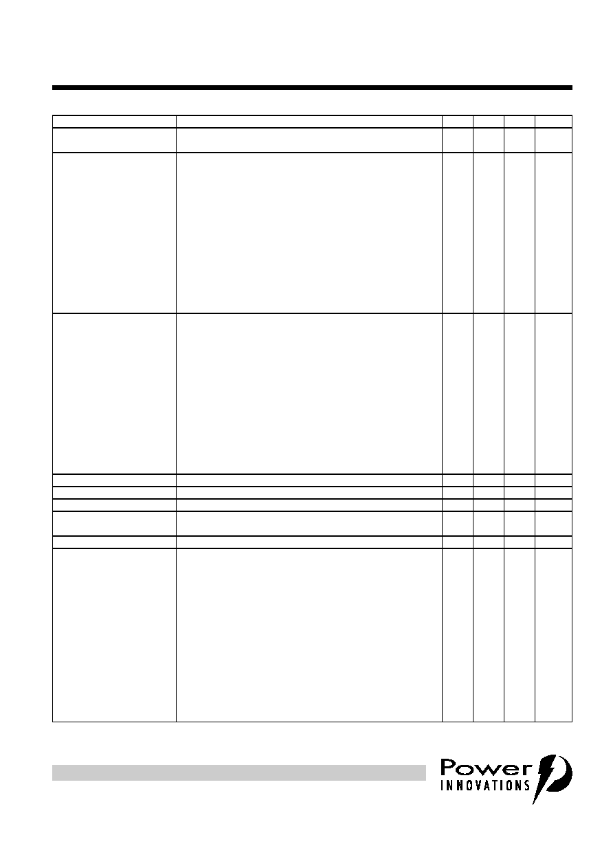
PARAMETER MEASUREMENT INFORMATION
Figure 1. VOLTAGE-CURRENT CHARACTERISTIC FOR T AND R TERMINALS
ALL MEASUREMENTS ARE REFERENCED TO THE R TERMINAL
-v
V
DRM
I
DRM
V
D
I
H
I
T
V
T
I
TSM
I
TSP
V
(BO)
I
(BO)
I
D
Quadrant I
Switching
Characteristic
+v
+i
V
(BO)
I
(BO)
V
D
I
D
I
H
I
T
V
T
I
TSM
I
TSP
-i
Quadrant III
Switching
Characteristic
PMXXAAB
V
DRM
I
DRM
5
NOVEMBER 1997 - REVISED MARCH 1999
TISP4070H3BJ THRU TISP4095H3BJ, TISP4125H3BJ THRU TISP4200H3BJ,
TISP4240H3BJ THRU TISP4400H3BJ
BIDIRECTIONAL THYRISTOR OVERVOLTAGE PROTECTORS
P R O D U C T I N F O R M A T I O N
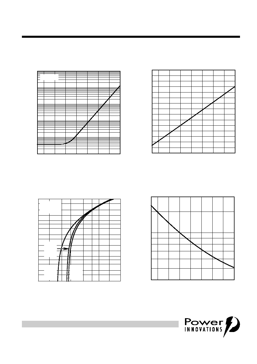
TYPICAL CHARACTERISTICS
Figure 2.
Figure 3.
Figure 4.
Figure 5.
OFF-STATE CURRENT
vs
JUNCTION TEMPERATURE
T
J
- Junction Temperature - ∞C
-25
0
25
50
75
100
125
150
|I
D
|
- Off
-
S
t
ate
Cu
rrent -
µ
A
0∑001
0∑01
0∑1
1
10
100
TCHAG
V
D
= ±50 V
NORMALISED BREAKOVER VOLTAGE
vs
JUNCTION TEMPERATURE
T
J
- Junction Temperature - ∞C
-25
0
25
50
75
100
125
150
No
rm
al
i
sed Break
o
v
er V
o
l
t
age
0.95
1.00
1.05
1.10
TC4HAF
ON-STATE CURRENT
vs
ON-STATE VOLTAGE
V
T
- On-State Voltage - V
0.7
1.5
2
3
4
5
7
1
10
I
T
-
On
-
S
t
a
te Cu
rren
t
- A
1.5
2
3
4
5
7
15
20
30
40
50
70
150
200
1
10
100
T
A
= 25 ∞C
t
W
= 100 µs
TC4HAC
'4070
THRU
'4095
'4125
THRU
'4200
'4240
THRU
'4400
NORMALISED HOLDING CURRENT
vs
JUNCTION TEMPERATURE
T
J
- Junction Temperature - ∞C
-25
0
25
50
75
100
125
150
No
r
m
a
l
i
s
e
d
Ho
l
d
i
n
g
Cu
rren
t
0.4
0.5
0.6
0.7
0.8
0.9
1.5
2.0
1.0
TC4HAD