
PACKAGE DIMENSIONS
0.173 (4.39)
0.120 (3.05)
0.240 (6.10)
0.183 (4.65)
0.500 (12.7)
MIN
0.020 (0.51)
SQ. (4X)
0.100 (2.54)
0.083 (2.11)
OPTICAL
CENTERLINE
PIN 1 COLLECTOR
PIN 2 EMITTER
PIN 4 CATHODE
PIN 3 ANODE
PIN 1 INDICATOR
0.083 (2.11)
3
4
2
1
NOTES:
1. Dimensions for all drawings are in inches (millimeters).
2. Tolerance of ± .010 (.25) on all non-nominal dimensions
unless otherwise specified.
3. Pins 2 and 4 typically .050" shorter than pins 1 and 3.
4. Dimensions controlled at housing surface.
NOTES
(Applies to Max Ratings and Characteristics Tables.)
1. Derate power dissipation linearly 1.33 mW/∞C above 25∞C.
2. RMA flux is recommended.
3. Methanol or isopropyl alcohols are recommended as cleaning
agents.
4. Soldering iron
1/16"
(1.6mm) from housing.
5. As long as leads are not under any spring tension.
6. D is the distance from the sensor face to the reflective surface.
7. Cross talk (I
CX
) is the collector current measured with the
indicator current on the input diode and with no reflective surface.
8. Measured using an Eastman Kodak neutral white test card with
90% diffused reflecting as a reflective surface.
1 of 3
100030A
QRD1113/1114
REFLECTIVE OBJECT SENSOR
FEATURES
∑ Phototransistor Output
∑ No contact surface sensing
∑ Unfocused for sensing diffused surfaces
∑ Compact Package
∑ Daylight filter on sensor
1
4
2
3
SCHEMATIC
Parameter
Symbol
Rating
Units
Operating Temperature
T
OPR
-40 to +85
∞C
Storage Temperature
T
STG
-40 to +85
∞C
Lead Temperature (Solder Iron)
(2,3)
T
SOL-I
240 for 5 sec
∞C
Lead Temperature (Solder Flow)
(2,3)
T
SOL-F
260 for 10 sec
∞C
EMITTER
Continuous Forward Current
I
F
50
mA
Reverse Voltage
V
R
5
V
Power Dissipation
(1)
P
D
100
mW
SENSOR
Collector-Emitter Voltage
V
CEO
30
V
Emitter-Collector Voltage
V
ECO
V
Power Dissipation
(1)
P
D
100
mW
ABSOLUTE MAXIMUM RATINGS
(T
A
= 25∞C unless otherwise specified)

PARAMETER
TEST CONDITIONS
SYMBOL
MIN
TYP
MAX
UNITS
EMITTER
I
F
= 20 mA
V
F
--
--
1.7
V
Forward Voltage
Reverse Current
V
R
= 5 V
I
R
--
--
100
µA
Peak Emission Wavelength
I
F
= 20 mA
!
PE
--
940
--
nm
SENSOR
I
C
= 1 mA
BV
CEO
30
--
--
V
Collector-Emitter Breakdown
Emitter-Collector Breakdown
I
E
= 0.1 mA
BV
ECO
5
--
--
V
Dark Current
V
CE
= 10 V, I
F
= 0 mA
I
D
--
--
100
nA
COUPLED
I
F
= 20 mA, V
CE
= 5 V
I
C(ON)
0.300
--
--
mA
QRD1113 Collector Current
D = .050"
(6,8)
QRD1114 Collector Current
I
F
= 20 mA, V
CE
= 5 V
I
C(ON)
1
--
--
mA
D = .050"
(6,8)
Collector Emitter
I
F
= 40 mA, I
C
= 100 µA
V
CE (SAT)
--
--
0.4
V
Saturation Voltage
D = .050"
(6,8)
Cross Talk
I
F
= 20 mA, V
CE
= 5 V, E
E
= 0
(7)
I
CX
--
.200
10
µA
Rise Time
V
CE
= 5 V, R
L
= 100
"
t
r
--
10
--
µs
Fall Time
I
C(ON)
= 5 mA
t
f
--
50
--
µs
ELECTRICAL / OPTICAL CHARACTERISTICS
(T
A
= 25∞C)
2 of 3
100030A
QRD1113/1114
REFLECTIVE OBJECT SENSOR
3 of 3
100030A
QRD1113/1114
REFLECTIVE OBJECT SENSOR
I
F
- FORWARD CURRENT (mA)
I
F
- FORWARD CURRENT (mA)
T
A
- AMBIENT TEMPERATURE (∞C)
T
A
- AMBIENT TEMPERATURE (∞C)
REFLECTIVE SURFACE DISTANCE (mils)
V
F
- FOR
W
ARD
V
O
L
T
A
GE (mA)
I
D
- COLLECT
OR D
ARK CURRENT
NORMALIZED - COLLECT
OR CURRENT (mA)
I
C
- COLLECT
OR CURRENT (mA)
I
C
- COLLECT
OR CURRENT (mA)
1.60
10.0
1.0
0.8
0.6
0.4
0.2
0
1.00
0.10
0.01
.001
1.0
.9
0
-50
-25
25
50
75
0
-50
-25
25
50
75
100
0
10
20
30
40
50
1.40
1.20
1.00
0.20
0.60
0.40
0.20
0.1
10
2
10
1
10
1.0
10
-1
10
-2
10
-3
1.0
10
100
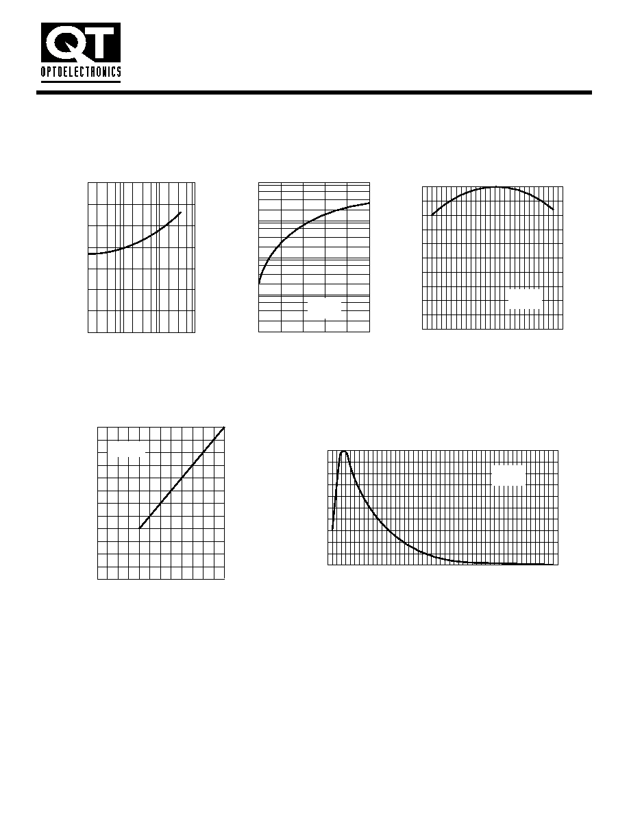
Fig. 1 Forward Voltage vs.
Forward Current
Fig. 2 Normalized Collector Current vs.
Forward Current
Fig. 3 Normalized Collector Current vs.
Temperature
Fig. 4 Normalized Collector Dark Current vs.
Temperature
Fig. 5 Normalized Collector Current vs.
Distance
I
F
= 10 mA
V
CE
= 5 V
.8
.7
.6
.5
.4
.3
.2
.1
0
0
50
100
150
200
250
300
350
400
450
500
V
CE
= 5 V
D = .05"
I
F
= 20 mA
V
CE
= 5 V
V
CE
= 10 V
TYPICAL PERFORMANCE CURVES