Raytheon RF Components
362 Lowell Street
Andover, MA 01810
Revised June 27, 2003
Page 1
www.raytheonrf.com
Specifications are based on most current or latest revision.
ADVANCED INFORMATION
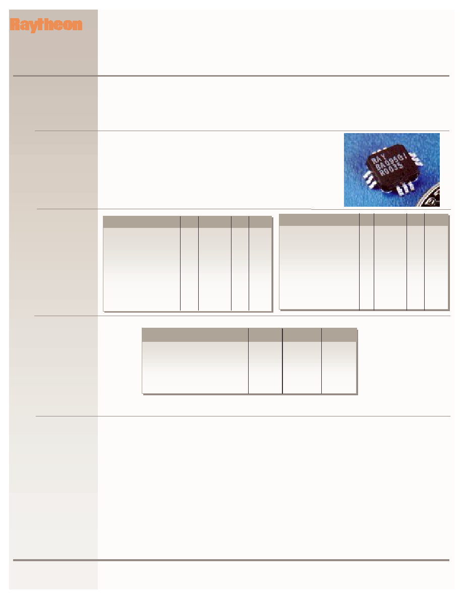
RMBA09501A-58
-
Cellular 2 Watt Linear GaAs
MMIC Power Amplifier
RF Components
The RMBA09501A is a high power, highly linear Power Amplifier. The two stage circuit uses Raytheon
RF Components' pHEMT process. It is designed for use as a driver stage for Cellular base stations, or
as the output stage for Micro- and Pico-Cell base stations. The amplifier has been optimized for high
linearity requirements for CDMA operation.
Description
Absolute
Ratings
Electrical
Characteristics
2
!
2 Watt Linear output power at 36 dBc ACPR1 for CDMA operation
!
OIP3
43 dBc at 27 and 30 dBm power output
!
Small Signal Gain of > 30 dB
!
Small outline SMD package
Features
Notes:
1. Only under quiescent conditions � no RF applied.
2. V
DD
= 7.0V, T
c
= 25�C. Part mounted on evaluation board with input and output matching to 50 Ohms.
3. 9 Channel Forward Link QPSK Source; 1.23 Mbps modulation rate. CDMA ACPR1 is measured using the ratio of the
average power within the 1.23 MHz channel at band center to the average power within a 30 KHz bandwidth at an 885
KHz offset. Minimum CDMA output power is met with ACPR1 > 36 dBc.
4. OIP3 specifications are achieved for power output levels of 27 and 30 dBm per tone with tone spacing of 1.25 MHz at
band-center.
5. VG1 and VG2 must be individually adjusted to achieve IDQ1 and IDQ2. A single VGG bias supply adjusted to achieve
IDQTOTAL=550mA can be used with nearly equivalent performance. Values for IDQ1 and IDQ2 shown have been
optimized for CDMA operation. IDQ1 and IDQ2 (or IDQTOTAL) can be adjusted to optimize the linearity of the amplifier for
other modulation systems.
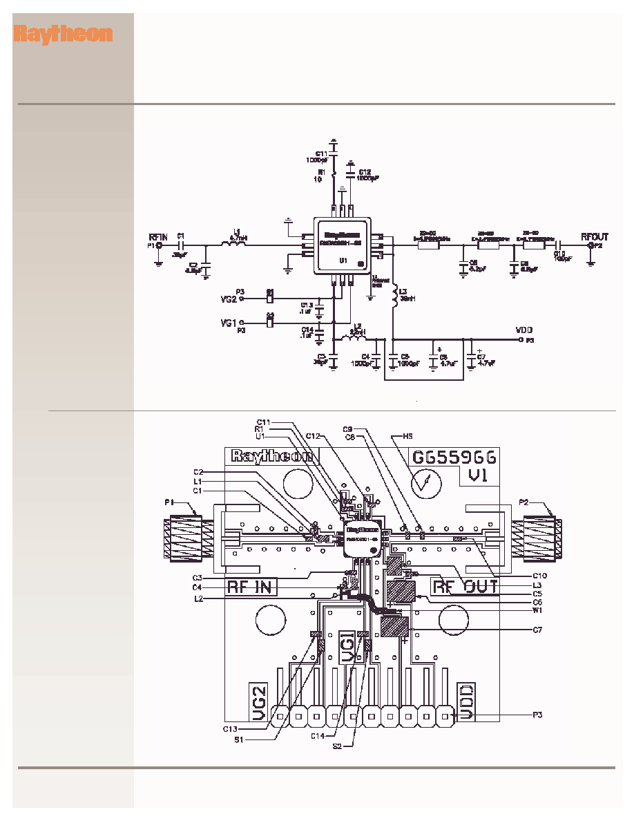
The device requires external input and output matching to 50 Ohms as shown in Figure 3 and the
Parts List.
Parameter
Symbol
Value
Unit
Drain Supply Voltage
1
Vdd
+10
V
Gate Supply Voltage
Vgs
-5
V
RF Input Power (from 50
source) Pin
5
dBm
Operating Case Temperature
Tc
-30 to +85
�C
Storage Temperature Range
Tstg
-40 to +100
�C
Parameter
Min
Typ
Max
Unit
Frequency Ranges
869
894
MHz
Gain (small signal)
30
35
dB
Gain variation:
Over frequency range
+/-1.5
dB
Over temperature range
+/-2.5
dB
Noise Figure
6
dB
Output power @ CDMA
3
33
dBm
OIP3
4
43
45
dBc
Parameter
Min
Typ
Max Unit
Idd@33 dBm Pout - 7V
1.0
A
PAE@33 dBm Pout
28.5
%
Input VSWR (50
)
2:1
Drain Voltage (Vdd)
7.0
Volts
Gate Voltage (VG
1
,VG
2
)
5
-2
-0.25 Volts
Quiescent currents
5
(IDQ1, IDQ2)
150, 400
mA
Thermal Resistance
(Channel to Case) Rjc
11
�C/W

Raytheon RF Components
362 Lowell Street
Andover, MA 01810
Revised June 27, 2003
Page 2
www.raytheonrf.com
Specifications are based on most current or latest revision.
ADVANCED INFORMATION
RMBA09501A-58
-
Cellular 2 Watt Linear GaAs
MMIC Power Amplifier
RF Components
CAUTION: THIS IS AN ESD SENSITIVE DEVICE
The following describes a procedure for evaluating the RMBA09501A-58, a monolithic high efficiency
power amplifier, in a surface mount package, designed for use as a driver stage for Cellular base
stations, or as the final output stage for Micro- and Pico-Cell base stations. Figure 1 shows the package
outline and the pin designations. Figure 2 shows the functional block diagram of the packaged product.
The RMBA09501A-58 requires external passive components for DC bias and RF input and output
matching circuits as shown in Figure 3 and the Parts List. A recommended schematic circuit is shown in
Figure 3. The gate biases for the two stages of the amplifier may be set by simple resistive voltage
dividers. Figure 4 shows a typical layout of an evaluation board, corresponding to the schematic circuits
of figure 3. The following designations should be noted:
(1) Pin designations are as shown in figure 1.
(2) Vg1 and Vg2 are the Gate Voltages (negative) applied at the pins of the package
(3) Vgg1 and Vgg2 are the negative supply voltages at the evaluation board terminals
(4) Vd1 and Vd2 are the Drain Voltages (positive) applied at the pins of the package
(5) Vdd1 and Vdd2 are the positive supply voltages at the evaluation board terminals
Note: The 2 terminals of Vdd1 and Vdd2 may be tied together.
The base of the package must be soldered on to a heat sink for proper operation.
Application
Information
AC Ground (g1)
Pin# 6
Figure 2
Functional Block
Diagram
RF IN
Pin# 8
RF OUT & Vd2
Pin# 1, 2, 3
Ground
Pin# 5, 7, 9, 13
Vg2
Pin# 11
AC Ground (g2)
Pin# 4
Vg1
Pin# 12
Vd1
Pin# 10
Figure 1
Package
Outline and
Pin
Designations
Dimensions in inches
Pin#
Description
1
RF Out & Vd2
2
RF Out & Vd2
3
RF Out & Vd2
4
AC Ground (g2)
5
GND
6
AC Ground (g1)
7
GND
8
RF In
9
GND
10
Vd1
11
Vg2
12
Vg1
13
GND
(Metal Base)
PLASTIC LID
SIDE SECTION
0.075 MAX.
0.010
0.230
0.246
0.282
1
2
3
5
4
6
7
9
8
10
12 11
0.041
1
2
3
0.015
0.200 SQ.
TOP VIEW
TOP VIEW
BOTTOM VIEW
5 4
6
7
9
8
10
12
11
0.030
RAY
RMBA
09501A
Vg1
Pin# 12
AC Ground (g1)
Pin#6

Raytheon RF Components
362 Lowell Street
Andover, MA 01810
Revised June 27, 2003
Page 4
www.raytheonrf.com
Specifications are based on most current or latest revision.
ADVANCED INFORMATION
RMBA09501A-58
-
Cellular 2 Watt Linear GaAs
MMIC Power Amplifier
RF Components
The following sequence must be followed to properly test the amplifier. (It is necessary to add a fan to
provide air cooling across the heat sink of RMBA09501A.) Note: Vdd1, 2 are tied together.
Test Procedure
for the evaluation
board (RMBA09501A-
58-TB)
Step 1: Turn off RF input power.
Step 2: Use GND terminal of the evaluation board
for the ground of the DC supplies. Slowly
apply gate supply voltages as specified on
results sheet supplied with test board to
the board terminals Vgg1 and Vgg2.
Step 3: Slowly apply drain supply voltages of
+7.0 V to the board terminals Vdd1, 2.
Adjust Vgg to set the total quiescent
current (with no RF applied) Idq as per
supplied result sheet. [Gate supply
voltages (Vgg i.e., Vgg1, Vgg2) may be
adjusted, only if quiescent current (Idq1
and Idq2) values desired are different
from those noted on the data summary
supplied with product samples].
Step 4: After the bias condition is established, RF
input signal may now be applied at the
appropriate frequency band and
appropriate power level.
Step 5:Follow turn-off sequence of:
(i) Turn off RF Input Power
(ii) Turn down and off drain voltages Vdd1,
2.
(iii) Turn down and off gate voltages Vgg1
and Vgg2.
Parts List
for Test Evaluation
Board (RMBA09501A-
58-TB)
CAUTION: LOSS OF GATE VOLTAGES (Vg1, Vg2) WHILE CORRESPONDING DRAIN
VOLTAGES (Vdd) ARE PRESENT CAN DAMAGE THE AMPLIFIER.
The PWB must be prepared with either an embedded copper slug in the board where the package is
to be mounted or a heat sink should be attached to the backside of the PWB where the package is to
be mounted on the front side. The slug or the heat sink should be made of a highly electrically and
thermally conductive material such as copper or aluminum. The slug should be at least the same
thickness as the PWB. In the case of the heat sink, a small pedestal should protrude through a hole in
the PWB where the package bottom is directly soldered. In either configuration, the top surface of the
slug or the pedestal should be made coplanar with the package lead mounting plane i.e., the top
surface of the PWB.
Use Sn96 solder (96.5% Sn and 3.5% Ag) at 220�C for 20 seconds or less to
attach the heat sink to the backside of the PWB. Then, using Sn63, the package bottom should be
firmly soldered to the slug or the pedestal while the pins are soldered to the respective pads on the
front side of the PWB without causing any stress on the pins. Remove flux completely if used for
soldering.
Thermal
Considerations
for Heat Sinking
the
RMBA09501A-58
Part
Value
EIA Size
Vendor(s)
C1,C3
39 pF
0402
Murata, GRM36COG390J050
C2,C9
6.8 pF
0402
Murata, GRM36COG6R8B050
C8
8.2 pF
0402
Murata, GRM36COG8R2B50
C4,C5,C11,C12 1000 pF
0402
Murata, GRM36X7R102K050
C6,C7
4.7 uF
3528
TDK, C3216X7R102K050
L1
4.7 nH
0603
Toko, LL1608-FH4N7S
L2
22 nH
0603
Toko, LL1608-FH22NK
L3
39 nH
1008
Coilcraft, 1008HQ-39NTKBC
R1
10 Ohm
0402
IMS, RCI-0402-10R0J
S1, S2
Bar or Ni Ribbon Short
W1
26AWG (0.015" dia) Wire
Alpha, 2853/1
U1
RMBA09501-58 PA
Raytheon
P3
Right angle Pin Header
3M 2340-5211TN
P1,P2
Brass SMA Connectors
Johnson Components 142-0701-841
Board
FR4
Raytheon Dwg# G654626, V1
C10
100 pF
0603
Murata, GRM36COG101J50
C13, C14
1.0 uF
0805
Murata, GRM39Y5V104Z50