 | –≠–ª–µ–∫—Ç—Ä–æ–Ω–Ω—ã–π –∫–æ–º–ø–æ–Ω–µ–Ω—Ç: RMDA00100 | –°–∫–∞—á–∞—Ç—å:  PDF PDF  ZIP ZIP |
Raytheon RF Components
362 Lowell Street
Andover, MA 01810
Revised June 12, 2002
www.raytheonrf.com
Characteristic performance data and specifications are subject to change
without notice.
ADVANCED INFORMATION
RMDA00100
OC-192 Modulator Driver MMIC
Description
Features
Notes:
1.
Off-chip decoupling and blocking capacitors required.
2.
All parameters met at T = 25∞C, V
d
= 8.0V, V
g2
=+1.5V, I
DQ
= 210mA.
3.
Measured in a 50 ohm system.
Absolute
Ratings
1
Parameter
Symbol
Min
Max
Unit
Supply Voltage
V
d
+8.0
V
RF Input Power
Pin
18
dBm
Case Operating Temperature
Tc
-40
+85
∞
C
Storage Temperature
Tstg
-40
+100
∞
C
The Raytheon RF Components RMDA00100 is a medium power broadband amplifier MMIC
suitable as a driver for external optical modulators for OC-192 fiber optic systems. It is available in
die form, and is manufactured using Raytheon RF Components' advanced 0.15µm pHEMT
process.
Applications include Long haul, Medium haul and Metro fiber systems
DC-20 GHz bandwidth
High gain: 15dB typ.
Low group delay
Gain control
Psat = 26dBm typ
Low power dissipation
Chip size 3.84 x 1.68 mm
Electrical
Characteristics
2,3
Parameter
Min
Typical
Max
Unit
3 dB Bandwidth (small signal)
17
GHz
Gain @ 10 GHz
15
dB
Output Power @ 10 GHz(saturated)
26
dBm
Group Delay
±20
pS
Output Voltage
8
V p-p
Input Return Loss
15
dB
Output Return Loss
10
dB
Gain control range
40
dB
Quiescent Current
210
mA
Vd
8.0
V
Vg
1
-0.3
V
Vg2 (Gain Control)
-1.5
+1.5
V

Raytheon RF Components
362 Lowell Street
Andover, MA 01810
Revised June 12, 2002
www.raytheonrf.com
Characteristic performance data and specifications are subject to change
without notice.
ADVANCED INFORMATION
RMDA00100
OC-192 Modulator Driver MMIC
Performance
Data
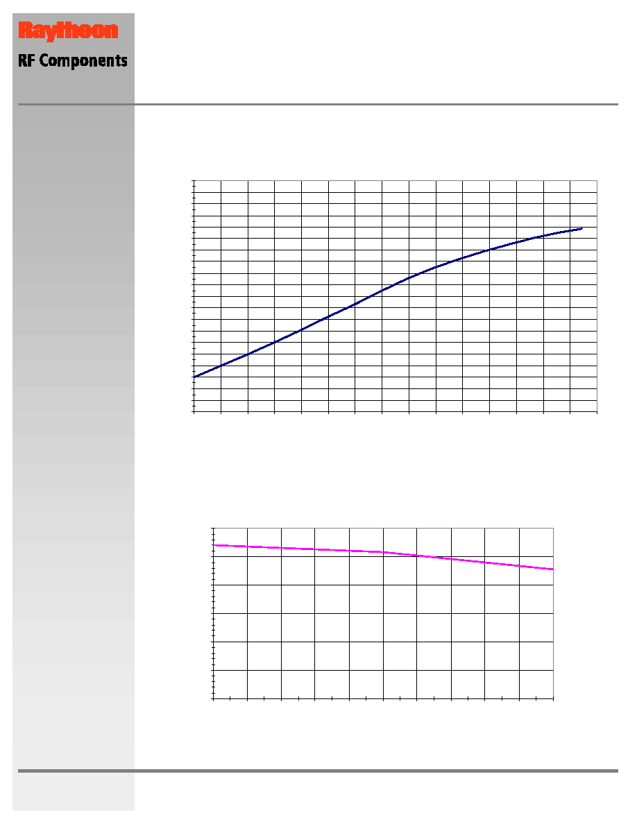
Small Signal Frequency Response
(Vds= 8.0, Id= 210 mA, Vg2 = +1.5V)
-35
-30
-25
-20
-15
-10
-5
0
5
10
15
20
0
5
10
15
20
25
Frequency (GHz)
dB
S11 dB
S21 dB
S22 dB
G ain C ontrol ( Vd=8V, v arious Vg2)
-3 0
-2 5
-2 0
-1 5
-1 0
-5
0
5
1 0
1 5
2 0
0
1
2
3
4
5
6
7
8
9
1 0
1 1
1 2
1 3
1 4
1 5
1 6
1 7
1 8
1 9
2 0
Fre q u e n cy (GHz )
G
a
in
(
d
B
)
V g 2 = 1.5
V g 2 = 0
V g 2 = -0.5
V g 2 = -0.75
Raytheon RF Components
362 Lowell Street
Andover, MA 01810
Revised June 12, 2002
www.raytheonrf.com
Characteristic performance data and specifications are subject to change
without notice.
ADVANCED INFORMATION
RMDA00100
OC-192 Modulator Driver MMIC
O utp ut P ow e r P 3db c vs F re q u e n cy o f Op e ra tion
(25C, Vd s=8.0, Id s=210m A, V g 2 = +1.5V)
0
5
10
15
20
25
30
5
6
7
8
9
10
11
12
13
14
15
F re q u e n cy (G Hz )
P
3
dB
c
/
dB
m
Pout VS Pin at 10 GHz
T= 25C, Vds=8.0, Ids=210mA, Vg2=+1.5V
10
11
12
13
14
15
16
17
18
19
20
21
22
23
24
25
26
27
28
29
30
0
1
2
3
4
5
6
7
8
9
10
11
12
13
14
15
Input Power (dBm)
Ou
tp
u
t
Po
we
r
(d
B
m
)
RMDA00100
OC-192 Modulator Driver MMIC
Raytheon RF Components
362 Lowell Street
Andover, MA 01810
Revised June 12, 2002
www.raytheonrf.com
Characteristic performance data and specifications are subject to change
without notice.
ADVANCED INFORMATION
RMDA00100
OC-192 Modulator Driver MMIC
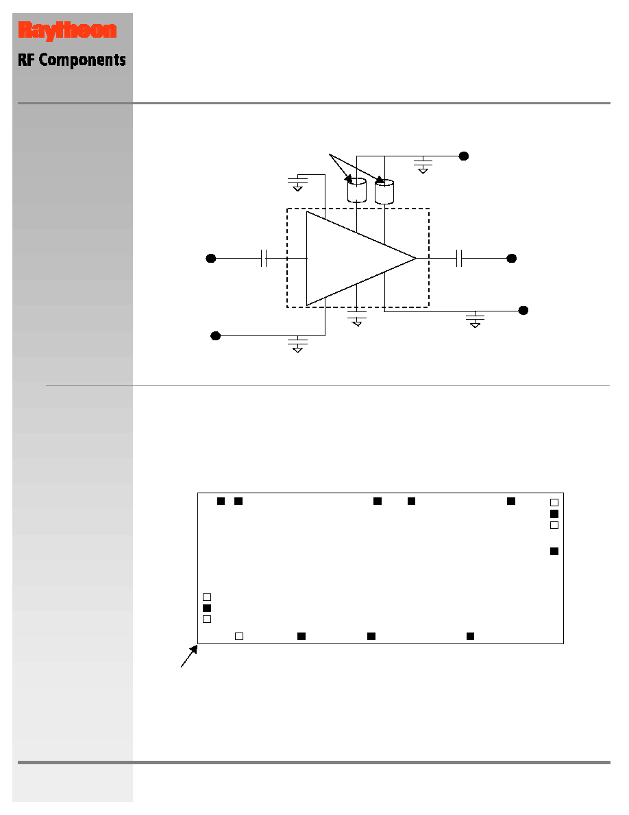
Recommended
Application
Schematic
Circuit
Diagram
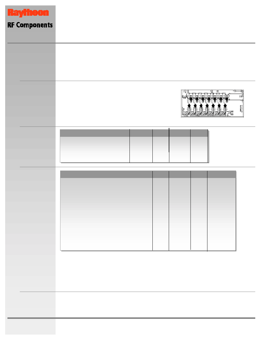
Chip Layout
and Bond Pad
Locations
Dimensions in mm
Caution: This is an ESD Sensitive Device
RMDA00100
OC-192 Modulator Driver MMIC
VDAUX
VD1
VD2
VD3
GND
RF OUT
VG2
VGAUX
VG1
VG3
GND
RF IN
(0.0 um, 0.0 um)
(
0
.
3
45
,
0.
09
)
(
1
.
0
9
,
0.
09
)
(
1
.
8
3
,
0.
09
)
(
2
.
8
7
,
0.
09
)
(3.753, 1.04)
(3.755, 1.43)
(
3
.
3
0
,
1.
59
)
(
2
.
2
5
,
1.
59
)
(
1
.
8
85
,
1.
59
)
(
0
.
4
24
,
1.
59
)
(
0
.
2
35
,
1.
59
)
(0.095, 0.342)
RF In
RF Out
10,000 pF
Vd
(+8V)
10,000 pF
Vg1
(-ve)
10,000 pF
3.3 pF
Broadband Spiral
inductors
~8
µ
H
VG1
VGAUX
VG2
VDAUX
VD1
VD2
Gain Control (Vg2)
10,000 pF
Raytheon RF Components
362 Lowell Street
Andover, MA 01810
Revised June 12, 2002
www.raytheonrf.com
Characteristic performance data and specifications are subject to change
without notice.
ADVANCED INFORMATION
RMDA00100
OC-192 Modulator Driver MMIC
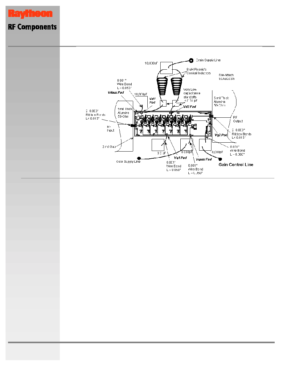
Recommended
Procedure for
Biasing and
Operation
Recommended
Assembly
Diagram
RMDA00100
OC-192 Modulator Driver MMIC
Caution: This is an ESD Sensitive Device.Loss of Gate Voltage (Vg
1
) while Drain Voltage (Vd) is
present may damage the amplifier chip.
The following sequence of steps must be followed to properly test the amplifier:
Step 1:
Turn off RF input power.
Step 2:
Connect the DC supply grounds to the ground of the chip carrier.
Apply negative gate bias supply voltage of ≠1.5 V to Vg
1
.
Step 3:
Apply +1.5V to Vg2 (Gain control).
Step 4:
Apply positive drain bias supply voltage of +8.0 V to Vd, and monitor drain current Id.
Step 5:
Adjust gate bias voltage Vg
1
to set the quiescent current of Idq ~ 210 mA.
Step 6:
After the bias condition is established, the RF input signal may now be
applied at the appropriate frequency band. Adjust Vg1 for best gain flatness.
Note:
When the device is under RF operation, the supply current Id will increase depending
upon output power required.
The gain can be adjusted from 15 dB to ≠35 dB by changing the voltage on Vg2 from
+1.5V to ≠1.0V
Step 7:
Follow turn-off sequence of:
(i) Turn off RF input power.
(ii) Turn down and off drain voltage (Vd).
(iii) Turn down and off Gain control voltage (Vg2).
(iv) Turn down and off gate bias voltage (Vg
1
).