Raytheon RF Components
362 Lowell Street
Andover, MA 01810
Revised February 6, 2003
Page 1
www.raytheonrf.com
Specifications are based on most current or latest revision.
PRODUCT INFORMATION
RMPA1956-103 - 3.5 V Dual Band Tri-Mode
AMPS, CDMA & CDMA2000-1X Power Amplifier
Module
RF Components
Operating Frequency
824
849
1850
1910
MHz
Gain at Po=28 dBm
30
24
dB
Linear Power Output
28
28
dBm
CDMA/CDMA2000-1X PAE
33
31
%
AMPS PAE,Pout=-31dBm
47
%
CDMA ACPR1
3
-50
-50
dBc
CDMA ACPR2
4
-60
-55
dBc
CDMA2000-1X ACPR1
-47
-47
dBc
CDMA2000-1X ACPR2
-55
-55
dBc
Noise Power (Po
28dBm)
-135
-135
dBm/Hz
Stability (all spurious)
5
-60
-60
dBc
Harmonics (Po
28dBm)
2fo, 3fo, 4fo
-30
-30
dBc
Power Shutdown Current
6
<1
<1
uA
Input VSWR (50 ohms)
2.0:1
2.0:1
Case Operating Temp.
-30
+85
-30
+85
o
C
Parameter
Cellular Band
PCS Band
Min Typical Max
Min Typical Max
Units
Description
!
Single positive-supply operation and power-down mode.
!
Operates in Cellular and PCS bands
!
33% power-added efficiency at +28 dBm CDMA average output power.
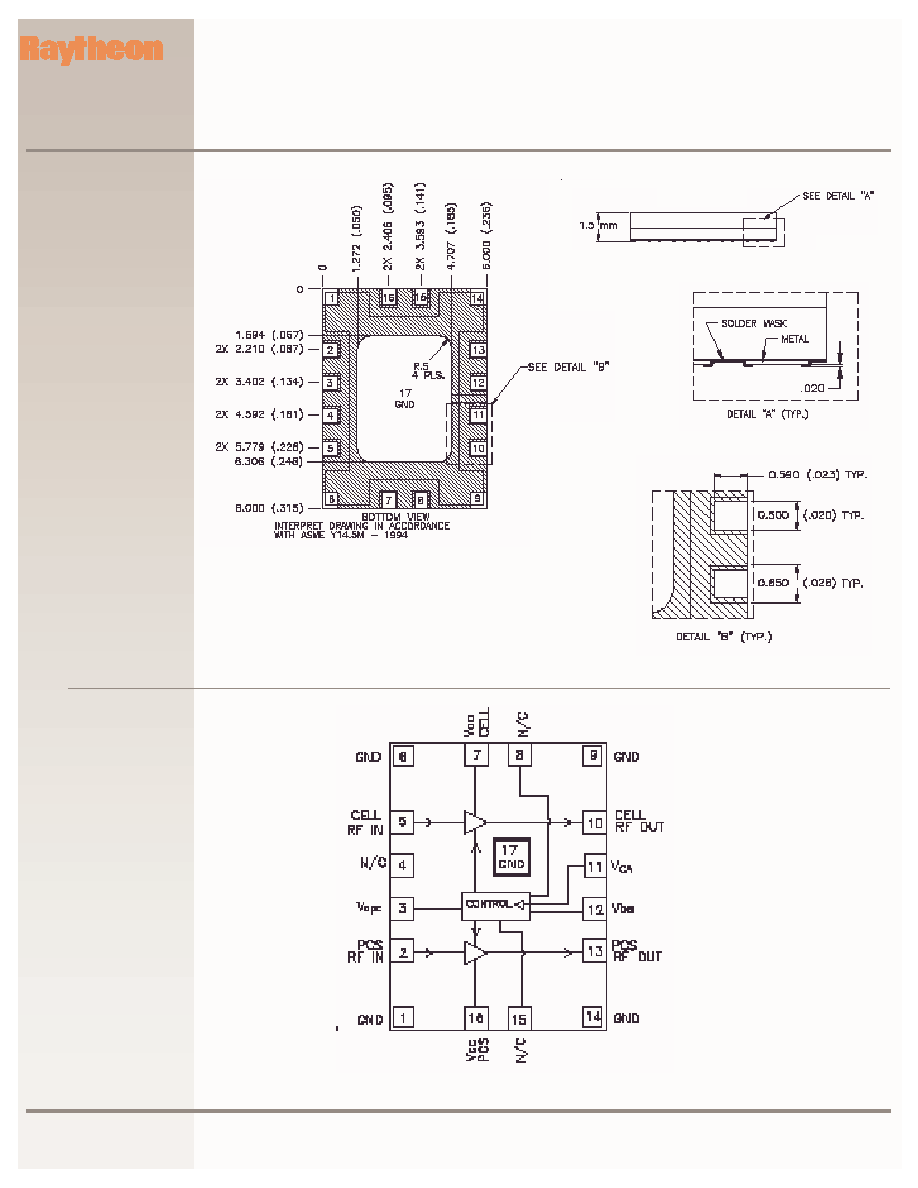
!
Compact LCC package- 6.0 x 8.0 x 1.5 mm
3
.
!
50 ohm matched and DC blocked input/output.
!
Advanced DC Power Management
Features
The RMPA1956-103 is a power amplifier for AMPS, CDMA and CDMA2000-1X personal
communications system (PCS) applications. The PA operates over both the Cellular and PCS bands.
The PA is internally matched to 50 ohms to minimize the use of external components. Advanced DC
power management reduces current consumption during peak phone usage at backed-off RF power
levels. High power-added efficiency and excellent linearity are achieved using Raytheon RF
Components' Heterojunction Bipolar Transistor (HBT) technology.
Electrical
Characteristics
2
Notes:
1. No permanent damage with only one parameter set at extreme limit. Other parameters set to typical values.
2. All parameters met at Tc =+25∞C, Vcc =+3.5V, f=1880 MHz and f=836.5 MHz, and load VSWR
1.2:1.
3. Po
28 dBm at Vcc=3.5V; CDMA Waveform measured using the ratio of average power within a
1.23 MHz channel to average power within a 30 kHz bandwidth at +/- 1.25 MHz offset at f=1880 MHz. Po
28 dBm at
Vcc=3.5V; CDMA Waveform measured using the ratio of average power within a
1.23 MHz channel to average power within a 30 kHz bandwidth at +/- 885 KHz offset at f=836.5 MHz
4. Po
28 dBm at Vcc=3.5V; CDMA Waveform measured using the ratio of average power within a
1.23 MHz channel to average power within a 30 kHz bandwidth at +/- 2.25 MHz offset at f= 1880 MHz. Po
28 dBm at
Vcc=3.5V; CDMA Waveform measured using the ratio of average power within a
1.23 MHz channel to average power within a 30 kHz bandwidth at +/- 1.98 MHz offset at f= 836.5 MHz
5. Output VSWR
6:1, all phase angles.
6. No applied RF signal. Vcc=+3.5V nominal, Vapc=+0.2V maximum.
Absolute
Ratings
1
Parameter
Symbol
Min
Max
Units
Supply Voltages
Vcc, Vca
5
V
Band Select Voltage
Vbs
3.0
V
Power Control Voltage
Vapc
0
3.0
V
RF Input Power
P
in
+5
dBm
Case Operating Temperature
T
c
-30
+85
∞
C
Storage Temperature
T
stg
-30
+85
∞
C

Raytheon RF Components
362 Lowell Street
Andover, MA 01810
Revised February 6, 2003
Page 3
www.raytheonrf.com
Specifications are based on most current or latest revision.
PRODUCT INFORMATION
RMPA1956-103 - 3.5 V Dual Band Tri-Mode
AMPS, CDMA & CDMA2000-1X Power Amplifier
Module
RF Components
Signal
Section Name
Description
Pin #
RF
Cell RF In
RF Input to Cell PA; DC blocked; 5 dBm
maximum input
5
PCS RF In RF Input to PCS PA; DC blocked; 5 dBm
maximum input
2
Cell RF Out RF Output of Cell PA; DC blocked
10
PCS RF
Out
RF Output of PCS PA; DC blocked
13
DC
Power
Vcc Cell
DC Supply for Final Stage Collector of
Cellular PA
7
Vcc PCS
DC Supply for Final Stage Collector of PCS
PA
16
Vca
DC Supply for Control Circuitry
11
These three DC Power signals may be tied
together in the phone.
Ground Gnd
Signal Ground
1,6,9,
14,17
Control Vbs
Band Switching
12
Vapc
Analog Power Control
3
Figure 3
Package Pinout
Raytheon RF Components
362 Lowell Street
Andover, MA 01810
Revised February 6, 2003
Page 4
www.raytheonrf.com
Specifications are based on most current or latest revision.
PRODUCT INFORMATION
RMPA1956-103 - 3.5 V Dual Band Tri-Mode
AMPS, CDMA & CDMA2000-1X Power Amplifier
Module
RF Components
2
Qty
Item #
P/N
Description
Vendor
1
1
G857345-1
PC Board
Raytheon
4
2
J1, J2
SMA Conn. Johnson
8
3
P1 or P2
Terminals
Samtec
1
4
G657342-1
RMPA1956
Raytheon
2
5
C321EDKSR1A335W
3.3uF Capacitor
TDK
4
3
5
1
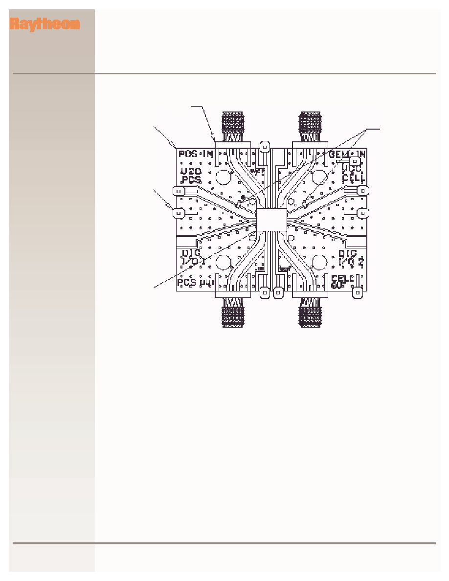
Figure 4
Evaluation
Board Layout
RMPA
1956
Raytheon RF Components
362 Lowell Street
Andover, MA 01810
Revised February 6, 2003
Page 5
www.raytheonrf.com
Specifications are based on most current or latest revision.
PRODUCT INFORMATION
RMPA1956-103 - 3.5 V Dual Band Tri-Mode
AMPS, CDMA & CDMA2000-1X Power Amplifier
Module
RF Components
Recommended Operating Conditions
Parameter
Symbol
Min
Typical
Max
Units
Supply Voltage
Vcc, Vca
3.1
3.5
4.5
V
RF Input Power
1
(either band)
Pin
0
+3
dBm
CDMA Output Power Range
Pout
-55
+28
dBm
Band Switch Voltage
Vbs
0
2
V
Analog Power Control
Vapc
0
2.6
V
Notes:
1.
Typical RF input power for CDMA Pout = +28dBm.
Figure 5
Electrical Specifications
Figure 6
Operational Control
Band & Power
Vcc
Vapc
Vbs
Cell
28 dBm
3.5V
2.6V
>2.0V
Cell
<28 dBm
3.5V
0.7 ≠ 2.0V
>2.0V
PCS
28 dBm
3.5V
2.6V
0V
PCS
<28 dBm
3.5V
0.7 ≠ 2.0V
0V
Shutdown
3.5V
0V
X