182
www.recom-international.com
April-2005
3 Watt
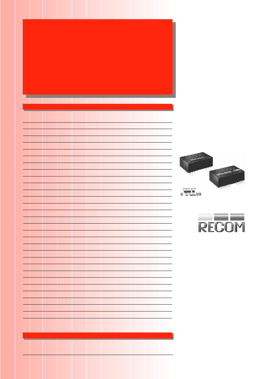
DIP24
&
&
SMD,
Single
&
&
Dual
Isolated Output
POWERLINE
DC/DC-Converter
RP03-S_DE
(DE/DS)
Series
2:1 Wide Input Voltage Range
3 Watts Regulated Output Power
1.6kVDC Isolation
Also Available with Isolated Outputs,
Output 1/Output 2 (DS) Isolation
Low Profile, 10.2 mm Height
Over Current Protection
Five-Sided Shield
No Derating to 71∞C
Non-Conductive Black Plastic
Standard DIP24 and SMD-Pinning
UL 1950 Component Recognized
High Efficiency to 80%
Features
Regulated
Converters
Selection Guide
5V, 12V, 24V and 48V Input Types
Part Number
Input Output
Output
Input
(4)
Efficiency
(5)
Capacitive
(6)
Range
Voltage
Current
Current Load max.
DIP24 (SMD)
VDC VDC mA mA %
µF
RP03-053.3SE**
4.5-6
3.3
600
638
66
2200
RP03-0505SE** 4.5-6
5
600
910
70
1000
RP03-0512SE** 4.5-6
12
250
845
75
170
RP03-0515SE** 4.5-6
15
200
845
75
110
RP03-123.3SE**
9-18
3.3
600
252
70
2200
RP03-1205SE** 9-18
5
600
352
75
1000
RP03-1212SE** 9-18
12
250
334
79
170
RP03-1215SE** 9-18
15
200
334
79
100
RP03-243.3SE** 18-36
3.3
600
126
70
2200
RP03-2405SE** 18-36
5
600
174
76
1000
RP03-2412SE** 18-36
12
250
165
80
170
RP03-2415SE** 18-36
15
200
165
80
100
RP03-483.3SE** 36-75
3.3
600
61
72
2200
RP03-4805SE** 36-75
5
600
88
75
1000
RP03-4812SE** 36-75
12
250
84
79
170
RP03-4815SE** 36-75
15
200
84
79
100
RP03-0505DE** 4.5-6
±5
±300
870
73
±500
RP03-0512DE** 4.5-6
±12
±125
845
75
±96
RP03-0515DE** 4.5-6
±15
±100
870
73
±47
RP03-1205DE** 9-18
±5
±300
357
74
±500
RP03-1212DE** 9-18
±12
±125
334
79
±96
RP03-1215DE** 9-18
±15
±100
334
79
±47
RP03-2405DE** 18-36
±5
±300
174
76
±500
RP03-2412DE** 18-36
±12
±125
167
79
±96
RP03-2415DE** 18-36
±15
±100
167
79
±47
RP03-4805DE** 36-75
±5
±300
86
77
±500
RP03-4812DE** 36-75
±12
±125
84
79
±96
RP03-4815DE** 36-75
±15
±100
84
79
±47
** add Suffix SMD for SMD package
Description
The E-Series of DC/DC Converters are fully certified to EN 60950: 2000. This makes them ideal for all
Telecom and safety applications where approved isolation is required.
They also meet UL 1950 and CSA 950 standards.
www.recom-international.com
183
April-2005
Selection Guide
5V, 12V, 24V and 48V Input Types
Specifications
(typical at nominal input and 25∞C unless otherwise noted)
POWERLINE
DC/DC-Converter
RP03-S_DE
(DE/DS) Series
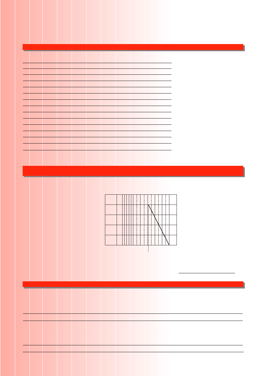
125
75
50
25
0
100
Ambient Temperature Range (∞C)
-25
-10 0
50 60 70 80 90 100
Output Power (%)
71
Natural Convection
RP03-4805SE
Input Voltage Range
5V nominal input
4.5-6VDC
12V nominal input
9-18VDC
24V nominal input
18-36VDC
48V nominal input
36-75VDC
Input Filter
Pi Type
Input Surge Voltage (100 ms max.)
5V Input
15VDC
12V Input
36VDC
24V Input
50VDC
48V Input
100VDC
continued on next page
Part Number
Input Output
Output
Input
(4)
Efficiency
(5)
Capacitive
(6)
Range
Voltage
Current
Current Load max.
for DE/DS(V1 & V2)
V1 & V2
V1 & V2
V1 & V2
DIP24 (SMD)
VDC VDC mA mA %
µF
RP03-0505DE/DS** 4.5-6
5 / 5
300 / 300
870
73
500 / 500
RP03-0512DE/DS** 4.5-6
12 / 12
125 / 125
845
75
96 / 96
RP03-0515DE/DS** 4.5-6
15 / 15
100 / 100
870
73
47 / 47
RP03-1205DE/DS** 9-18
5 / 5
300 / 300
357
74
500 / 500
RP03-1212DE/DS** 9-18
12 / 12
125 / 125
334
79
96 / 96
RP03-1215DE/DS** 9-18
15 / 15
100 / 100
334
78
47 / 47
RP03-2405DE/DS** 18-36
5 / 5
300 / 300
174
76
500 / 500
RP03-2412DE/DS** 18-36
12 / 12
125 / 125
167
79
96 / 96
RP03-2415DE/DS** 18-36
15 / 15
100 / 100
167
79
47 / 47
RP03-4805DE/DS** 36-75
5 / 5
300 / 300
86
77
500 / 500
RP03-4812DE/DS** 36-75
12 / 12
125 / 125
84
79
96 / 96
RP03-4815DE/DS** 36-75
15 / 15
100 / 100
84
79
47 / 47
** add Suffix SMD for SMD package
Derating-Graph
(Ambient Temperature)
Derating graphes are valid only for the shown part numbers. If you need detailed derating-information about a
part-number not shown here please contact our technical customer service at info@recom-development.at

184
www.recom-international.com
April-2005
Specifications
(typical at nominal input and 25∞C unless otherwise noted)
POWERLINE
DC/DC-Converter
RP03-S_DE
(DE/DS) Series
Input Reflected Ripple (nominal Vin and full load)
120mAp-p
Start Up Time (nominal Vin and constant resistor load)
30ms typ.
Output Power
3W max.
Output Voltage Accuracy (full Load and nominal Vin)
±2%
Minimum Load (see Note 1)
10% of FL
Line Regulation (LL-HL at full load)
±0.2%
DS
±0.5%
Load Regulation (25% to 100% FL)
Single
±0.2%
Dual
±2%
DS
±0.5%
Cross Regulation (asymmetrical load 25%/100% FL)
±5%
Ripple and Noise (20MHz bandwith)
3.3V, 5V
75mVp-p
others
1%/p-p of Vout max.
Temperature Coefficient
±0.02%/∞C, max.
Transient Response (25% load step change)
500µS
Over Load Protection (% of full load at nominal Vin)
180% typ
Short Circuit Protection
Continuous, automatic recovery
Efficiency
see ,,Selection Guide" table
Isolation Voltage
In to out
1.600VDC min.
Output to Output
/DS type 500VDC min.
Isolation Resistance
10
9
min.
Isolation Capacitance
300pF max.
Operating Frequency
100kHz min.
Approved to Safety Standards
UL 1950, EN60950
Operating Temperature Range
-25∞C to +71∞C
Storage Temperature Range
-55∞C to +105∞C
Vibration
10-55Hz, 2G, 30 Min. along X, Y and Z
Relative Humidity
5% to 95% RH
Case Material
Non-conductive black plastic
Base Material
Non-conductive black plastic
Potting Material
Epoxy (UL94-V0)
Conducted Emissions
EN55022
Level A
Radiated Emissions
EN55022
Level A
ESD
EN61000-4-2
Perf. Criteria 2
Radiated Immunity
EN61000-4-3
Perf. Criteria 2
Fast Transient
EN61000-4-4
Perf. Criteria 2
Surge
EN61000-4-5
Perf. Criteria 2
Conducted Immunity
EN61000-4-6
Perf. Criteria 2
Weight
DIP
14g
SMD
15g
Dimensions
DIP
31.8 x 20.3 x 10.2mm
SMD
32.0 x 20.3 x 10.9mm
MTBF (see note 2)
3.706 x 10
6
Hours
www.recom-international.com
185
April-2005
POWERLINE
DC/DC-Converter
Notes :
RP03-S_DE
(DE/DS) Series
Notes :
1. The RP03 series requires a minimum of 10% loading on the output to maintain specified regulation. Operation under
no-load condition will not damage these devices, however they may not meet all listed specification.
2. BELLCORE TR-NWT-000332. Case l: 50% Stress, Temperature at 40∞C (Ground fixed and controlled environment).
3. Should an O/O isolation be required, please order the converter with the following part number: RP03-XXXXDE/DS.
4. Maximum value at nominal input voltage and full load of standard type.
5. Typical value at nominal input voltage and full load.
6. Test by minimum Vin and constant resistor load.
7. See application notes for EMI-filtering.
DIP24 Package Style
2.54
22.90
2
10.20
0.25 x 0.50
Rectangular Pin
15.20
Bottom View
1 2 3
20.30
31.80
10 11 12
15 14 13
24 23 22
3.8
3rd angle
projection
Pin Pitch Tolerance ±0.35 mm
SMD Package Style
20.30
9 10 11 12
24 23 22
16 15 14 13
21 20
1
3
2
5
4
1
31.40
25.40
10.90
Bottom View
11 x 2.54
Pin area
0.1 x 0.50
0.50
32.00
11.20
2.54
24.14
27.94
26.54
1.60
2.40
Top View
21.30
3.81
6.35
2.54
23.40
SMD Package Style
Same spec. as the original DIP spec. and pin
definition, excl. of the SMD type pin.
Pin Connections
Pin #
Single
Dual
Dual
Separate
1
+ V in
+ V in
+ V in
2
NC
≠ V out
≠ V1 out
3
NC
Com
+ V1 out
10
- V out
Com
≠ V2 out
11
+ V out
+ V out
+ V2 out
12
≠ V in
≠ V in
≠ V in
13
≠ V in
≠ V in
≠ V in
14
+ V out
+ V out
+ V2 out
15
- V out
Com
≠ V2 out
22
NC
Com
+ V1 out
23
NC
- V out
≠ V1 out
24
+ V in
+ V in
+ V in
NC = No Connection
Pin Pitch Tolerance ±0.35 mm
Pin Connections
Pin #
Single
Dual
Dual
Separate
1
+ V in
+ V in
+ V in
2
NC
≠ V out
≠ V1 out
3
NC
Com
+ V1 out
10
- V out
Com
≠ V2 out
11
+ V out
+ V out
+ V2 out
12
≠ V in
≠ V in
≠ V in
13
≠ V in
≠ V in
≠ V in
14
+ V out
+ V out
+ V2 out
15
- V out
Com
≠ V2 out
22
NC
Com
+ V1 out
23
NC
- V out
≠ V1 out
24
+ V in
+ V in
+ V in
Others NC
NC NC
NC = No Connection