HZU-L Series
Rev.1.00, Jun.05.2003, page 5 of 8
Mark Code
Type
Grade
Mark No.
Type
Grade
Mark No.
Type
Grade
Mark No.
HZU6L
A1
61
HZU11L
A1
111
HZU20L
≠1
201
A2
62
A2
112
≠2
202
A3
63
A3
113
≠3
203
B1
64
B1
114
HZU22L
≠1
221
B2
65
B2
115
≠2
222
B3
66
B3
116
≠3
223
C1
67
C1
117
HZU24L
≠1
241
C2
68
C2
118
≠2
242
C3
69
C3
119
≠3
243
HZU6L
A1
71
HZU12L
A1
121
HZU27L
≠1
271
A2
72
A2
122
≠2
272
A3
73
A3
123
≠3
273
B1
74
B1
124
HZU30L
≠1
301
B2
75
B2
125
≠2
302
B3
76
B3
126
≠3
303
C1
77
C1
127
HZU33L
≠1
331
C2
78
C2
128
≠2
332
C3
79
C3
129
≠3
333
HZU9L
A1
91
HZU15L
≠1
151
HZU36L
≠1
361
A2
92
≠2
152
≠2
362
A3
93
≠3
153
≠3
363
B1
94
HZU16L
≠1
161
B2
95
≠2
162
B3
96
≠3
163
C1
97
HZU18L
≠1
181
C2
98
≠2
182
C3
99
≠3
183
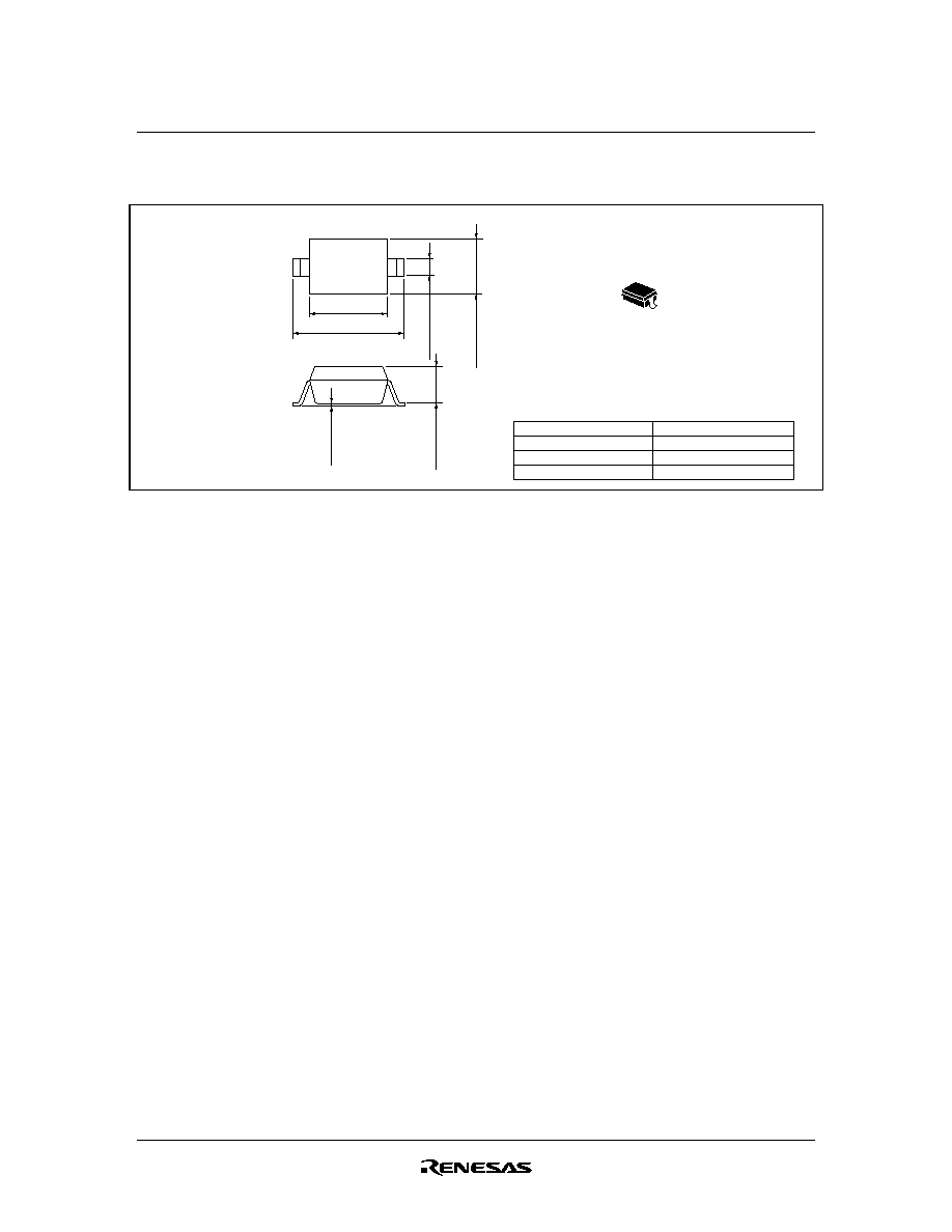
Notes: 1. Example of Marking
(1) HZU6A1L to HZU9C3L Example of Marking
(2) HZU11A1L to HZU36-3L Example of Marking
HZU6A1L
61
111
HZU11A1L
2. Type No. is as follows; HZU6A1L, HZU6A2L, ∑∑∑ HZU12C3L
3. Type No. is as follows; HZU15 ≠ 1L, HZU15 ≠ 2L, ∑∑∑ HZU36 ≠ 3L

HZU-L Series
Rev.1.00, Jun.05.2003, page 8 of 8
Keep safety first in your circuit designs!
1. Renesas Technology Corporation puts the maximum effort into making semiconductor products better and more reliable, but there is always the possibility that trouble may occur with
them. Trouble with semiconductors may lead to personal injury, fire or property damage.
Remember to give due consideration to safety when making your circuit designs, with appropriate measures such as (i) placement of substitutive, auxiliary circuits, (ii) use of
nonflammable material or (iii) prevention against any malfunction or mishap.
Notes regarding these materials
1. These materials are intended as a reference to assist our customers in the selection of the Renesas Technology Corporation product best suited to the customer's application; they
do not convey any license under any intellectual property rights, or any other rights, belonging to Renesas Technology Corporation or a third party.
2. Renesas Technology Corporation assumes no responsibility for any damage, or infringement of any third-party's rights, originating in the use of any product data, diagrams, charts,
programs, algorithms, or circuit application examples contained in these materials.
3. All information contained in these materials, including product data, diagrams, charts, programs and algorithms represents information on products at the time of publication of these
materials, and are subject to change by Renesas Technology Corporation without notice due to product improvements or other reasons. It is therefore recommended that customers
contact Renesas Technology Corporation or an authorized Renesas Technology Corporation product distributor for the latest product information before purchasing a product listed
herein.
The information described here may contain technical inaccuracies or typographical errors.
Renesas Technology Corporation assumes no responsibility for any damage, liability, or other loss rising from these inaccuracies or errors.
Please also pay attention to information published by Renesas Technology Corporation by various means, including the Renesas Technology Corporation Semiconductor home page
(http://www.renesas.com).
4. When using any or all of the information contained in these materials, including product data, diagrams, charts, programs, and algorithms, please be sure to evaluate all information
as a total system before making a final decision on the applicability of the information and products. Renesas Technology Corporation assumes no responsibility for any damage,
liability or other loss resulting from the information contained herein.
5. Renesas Technology Corporation semiconductors are not designed or manufactured for use in a device or system that is used under circumstances in which human life is potentially
at stake. Please contact Renesas Technology Corporation or an authorized Renesas Technology Corporation product distributor when considering the use of a product contained
herein for any specific purposes, such as apparatus or systems for transportation, vehicular, medical, aerospace, nuclear, or undersea repeater use.
6. The prior written approval of Renesas Technology Corporation is necessary to reprint or reproduce in whole or in part these materials.
7. If these products or technologies are subject to the Japanese export control restrictions, they must be exported under a license from the Japanese government and cannot be
imported into a country other than the approved destination.
Any diversion or reexport contrary to the export control laws and regulations of Japan and/or the country of destination is prohibited.
8. Please contact Renesas Technology Corporation for further details on these materials or the products contained therein.
Sales Strategic Planning Div. Nippon Bldg., 2-6-2, Ohte-machi, Chiyoda-ku, Tokyo 100-0004, Japan
http://www.renesas.com
Copyright © 2003. Renesas Technology Corporation, All rights reserved. Printed in Japan.
Colophon 0.0