
Regarding the change of names mentioned in the document, such as Mitsubishi
Electric and Mitsubishi XX, to Renesas Technology Corp.
The semiconductor operations of Hitachi and Mitsubishi Electric were transferred to Renesas
Technology Corporation on April 1st 2003. These operations include microcomputer, logic, analog
and discrete devices, and memory chips other than DRAMs (flash memory, SRAMs etc.)
Accordingly, although Mitsubishi Electric, Mitsubishi Electric Corporation, Mitsubishi
Semiconductors, and other Mitsubishi brand names are mentioned in the document, these names
have in fact all been changed to Renesas Technology Corp. Thank you for your understanding.
Except for our corporate trademark, logo and corporate statement, no changes whatsoever have been
made to the contents of the document, and these changes do not constitute any alteration to the
contents of the document itself.
Note : Mitsubishi Electric will continue the business operations of high frequency & optical devices
and power devices.
Renesas Technology Corp.
Customer Support Dept.
April 1, 2003
To all our customers

2002-07-12 Rev.1.0
Mitsubishi Microcomputers
32180 Group
Under Development
SINGLE-CHIP 32-BIT CMOS MICROCOMPUTER
Description
The 32180 Group is a 32-bit, single-chip RISC microcom-
puter with built-in flash memory, which was developed for
use in general industrial and household equipment. To ac-
complish high-precision arithmetic operations, it incorpo-
rates a fully IEEE754 compliant, single-precision FPU.
This microcomputer contains a variety of peripheral func-
tions ranging from two independent blocks of 16-channel A-
D converters to 64-channel multifunction timers, 10-channel
DMACs, 6-channel serial I/Os, and 1-channel real-time de-
bugger. Also included are 2-channel Full-CAN modules and
JTAG (boundary scan facility). With the software necessary
to run these numerous peripheral functions stored in its
large-capacity flash memory, this microcomputer meets the
needs of application systems for high functionality, high-
performance arithmetic capability, and sophisticated control.
With lower power consumption and low noise characteris-
tics also considered, these microcomputers are ideal for
embedded equipment applications.
Features
M32R-FPU core
∑ Uses the M32R family RISC CPU core (M32R family
common instruction set + single-precision FPU/extended
instructions)
∑ Five-stage pipelined processing
∑ Sixteen 32-bit general-purpose registers
∑ 16-bit/32-bit instructions implemented
∑ DSP function instructions (sum-of-products calculation
using 56-bit accumulator)
∑ Built-in single-precision FPU (fully compliant with IEEE754
standard: four rounding modes, etc.)
∑ Bit manipulation extended instructions
∑ Built-in flash memory .....................1M bytes (1024K bytes)
∑ Built-in flash programming boot program
∑ Built-in RAM ....................................................... 48K bytes
∑ PLL clock generating circuit.............. Built-in x 8 PLL circuit
∑ Oscillation stop detection function
∑ Maximum operating frequency of the CPU clock
Type Name
Frequency
Temperature range
M32180F8VFP
64MHz
-40∞C to +125∞C
M32180F8TFP
80MHz
-40∞C to +85∞C
∑ Single power supply: 5 V (+ 0.5 V) or 3.3 V (+ 0.3 V)
64-channel multijunction timers (MJT)
Multifunction timers are incorporated that support various
purposes of use.
16-bit output related timers (TOP) ................... 11 channels
16-bit input/output related timers (TIO)............ 10 channels
16-bit input related timers (TMS) ....................... 8 channels
16-bit input related up/down-timers (TID) .......... 3 channels
24-bit output related timers (TOU)................... 24 channels
32-bit input related timers (TML) ....................... 8 channels
∑ Flexible configuration is possible through interconnection
of timers.
∑ The internal DMAC and A-D converter can be started by a
timer.
∑ Built-in PWM output cut function for motor control (TOU)
Real-time Debugger
∑ Includes dedicated clock-synchronized serial I/O that can
read and write the contents of the internal RAM independ-
ently of the CPU.
∑ Can look up and update the data table in real time while
the program is running.
∑ Can generate a dedicated interrupt based on RTD com-
munication.
Abundant internal peripheral functions
In addition to the timers and real-time debugger, the micro-
computer contains the following peripheral functions.
∑ DMAC ............................................................. 10 channels
∑ A-D converters (Sample & hold mode, Disconnection de-
tector assist function, Injection current bypass circuit)
................................16 channels 10-bit converter x 2
∑ Serial I/O ........................................................... 6 channels
∑ Interrupt controller: 32 interrupt sources, 8 priority levels
∑ Wait controller
∑ Full CAN (CAN Specification 2.0B active)......... 2 channels
∑ Virtual-Flash emulation function .......... 4K bytes x 8 banks
∑ JTAG (boundary scan function, Mitsubishi original SDI
debug function)
∑ Port input threshold level select function
Designed to operate at high temperatures
To meet the need for use at high temperatures,
M32180F8VFP is designed to be able to operate in the
temperature range of -40 to +125∞C when CPU clock oper-
ating frequency = 64 MHz. M32180F8TFP is designed to be
able to operate in the temperature range of ≠40 to +85∞C
when CPU clock operating frequency = 80 MHz.
Applications
Automobile equipment control (e.g., Engine, ABS, and AT),
industrial equipment system control, and high-function OA
equipment (e.g., PPC)
2002-07-12 Rev.1.0
Mitsubishi Microcomputers
32180 Group
Under Development
SINGLE-CHIP 32-BIT CMOS MICROCOMPUTER
2
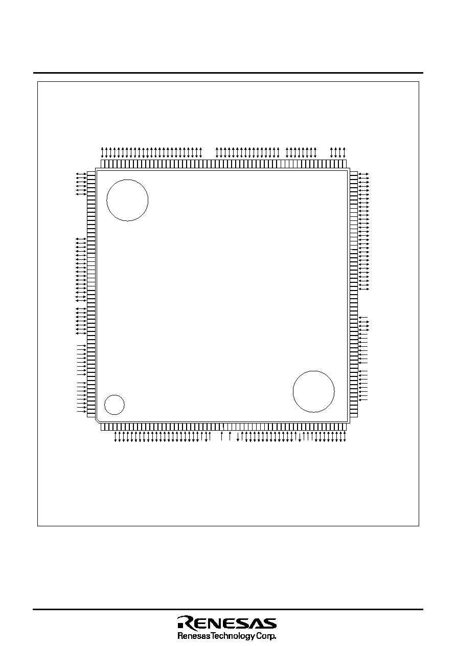
P174/TXD2
P175/RXD2
P176/TXD3
P177/RXD3
P173/TIN25
P172/TIN24
FP
MOD0
MOD1
EXCVDD
VSS
EXCVCC
VDDE
VSS
VCCE
VCC-BUS
P17/DB15
P16/DB14
P15/DB13
P14/DB12
P13/DB11
P12/DB10
P11/DB9
P10/DB8
P07/DB7
P06/DB6
P05/DB5
P04/DB4
P03/DB3
P02/DB2
P01/DB1
P00/DB0
VSS
P73/HACK#
P72/HREQ#
P71/WAIT#
P70/BCLK/WR#
P43/RD#
P42/BHW#/BHE#
P41/BLW#/BLE#
VCC-BUS
VSS
AD1IN15
AD1IN14
AD1IN13
AD1IN12
AD1IN11
AD1IN10
AD1IN9
AD1IN8
AVSS1
AD1IN7
AD1IN6
AD1IN5
AD1IN4
AD1IN3
AD1IN2
AD1IN1
AD1IN0
VREF1
P82/TXD0
P83/RXD0
P84/SCLKI0/SCLKO0
P85/TXD1
P86/RXD1
P87/SCLKI1/SCLKO1
P65/SCLKI4/SCLKO4
P66/SCLKI5/SCLKO5
P67
P210/TO37
P211/TO38
P212/TO39
P213/TO40
P214/TO41
P215/TO42
P216/TO43
P217/TO44
P160/TO21
P161/TO22
P162/TO23
P163/TO24
P164/TO25
P165/TO26
P166/TO27
P167/TO28
VSS
VCCE
VCC-BUS
P226/CS2#
P227/CS3#
P44/CS0#
P45/CS1#
P224/A11/CS2#
P225/A12/CS3#
P46/A13
P47/A14
P30/A15
P31/A16
P32/A17
P33/A18
P34/A19
P35/A20
P36/A21
P37/A22
VSS
P20/A23
P21/A24
P22/A25
P23/A26
P24/A27
P25/A28
P26/A29
P27/A30
VCC-BUS
VSS
VCCE
P93/TO16
P94/TO17
P95/TO18
P96/TO19
M32180F8VFP
M32180F8TFP
181
182
183
184
185
186
187
188
189
190
191
192
193
194
195
196
197
198
199
200
201
202
203
204
205
206
207
208
209
210
211
212
213
214
215
216
217
218
219
220
221
222
223
224
225
226
227
228
229
230
231
232
233
234
235
236
237
238
239
240
120
119
118
117
116
115
114
113
112
111
110
109
108
107
106
105
104
103
102
101
100
99
98
97
96
95
94
93
92
91
90
89
88
87
86
85
84
83
82
81
80
79
78
77
76
75
74
73
72
71
70
69
68
67
66
65
64
63
62
61
1
2
3
4
5
6
7
8
9
10
11
12
13
14
15
16
17
18
19
20
21
22
23
24
25
26
27
28
29
30
31
32
33
34
35
36
37
38
39
40
41
42
43
44
45
46
47
48
49
50
51
52
53
54
55
56
57
58
59
60
180
179
178
177
176
175
174
173
172
171
170
169
168
167
166
165
164
163
162
161
160
159
158
157
156
155
154
153
152
151
150
149
148
147
146
145
144
143
142
141
140
139
138
137
136
135
134
133
132
131
130
129
128
127
126
125
124
123
122
121
Package 240P6Y-A(0.5mm pitches)
AVCC1
VSS
VCCE
P150/TIN0
P151/TIN1
P152/TIN2
P153/TIN3
P154/TIN4
P155/TIN5
P156/TIN6
P157/TIN7
P200/TXD4
P201/RXD4
P202/TXD5
P203/RXD5
P130/TIN16/PWMOFF0
P131/TIN17/PWMOFF1
P132/TIN18
P133/TIN19
P134/TIN20
P135/TIN21
P136/TIN22
P137/TIN23
P220/CTX0
P221/CRX0
P222/CTX1
P223/CRX1
VCCE
OSC-VSS
VCNT
OSC-VCC
XIN
OSC-VSS
XOUT
RESET#
P180/TO29
P181/TO30
P182/TO31
P183/TO32
P184/TO33
P185/TO34
P186/TO35
P187/TO36
P74/RTDTXD
P75/RTDRXD
P76/RTDACK
P77/RTDCLK
JTDI
JTDO
JTRST
JTCK
JTMS
P100/TO8
P101/TO9/TXD3
P102/TO10/CTX1
P103/TO11
P104/TO12
P105/TO13
P106/TO14
P107/TO15
P97/TO20
P117/TO7
P116/TO6
P115/TO5
P114/TO4
P113/TO3
P112/TO2
P111/TO1
P110/TO0
P147/TIN15
P146/TIN14
P145/TIN13
P144/TIN12
P143/TIN11
P142/TIN10
P141/TIN9
P140/TIN8
P197/TIN33/PWMOFF2
P196/TIN32
P195/TIN31
P194/TIN30
P193/TIN29
P192/TIN28
P191/TIN27
P190/TIN26
P127/TCLK3
P126/TCLK2
P125/TCLK1
P124/TCLK0
EXCVCC
VSS
VCCE
VSS
VSS
VSS
SBI#
P63
P62
P61
AD0IN15
AD0IN14
AD0IN13
AD0IN12
AD0IN11
AD0IN10
AD0IN9
AD0IN8
AVSS0
AD0IN7
AD0IN6
AD0IN5
AD0IN4
AD0IN3
AD0IN2
AD0IN1
AD0IN0
VREF0
AVCC0
VSS
VCCE
Note: It is shown that the pin (signal) with which "#" sticks to the last of a pin name (signal name) is "L" active pin (signal).
Pin Assignment(top view)
Figure 1. Pin Layout Diagram

2002-07-12 Rev.1.0
Mitsubishi Microcomputers
32180 Group
Under Development
SINGLE-CHIP 32-BIT CMOS MICROCOMPUTER
3
PLL clock generation
circuit
Internal bus
interface
Address
Data
Internal RAM
(48K bytes)
Internal flash memory
(1M bytes=1024K bytes)
M32R-FPU core
(max. 80MHz)
Multiplier accumulator
(32x16+56)
DMAC
(10 channels)
Input/output timer
(64 channels)
Serial I/O
(6 channels)
A-D converter x 2
(A-D0 : 10-bit,16 channels)
(A-D1 : 10-bit,16 channels)
Wait controller
Interupt controller
(8 priority levels)
Real-time debugger
(RTD)
External bus
interface
Internal
32-bit bus
Input/output port 158 ports
Full CAN
(2 channels)
Single-precision FPU
(fully IEEE754 compliant)
Internal
16-bit bus
Internal
32-bit bus
Internal power supply
generation circuit
(VDC)
Figure 2. Block diagram

2002-07-12 Rev.1.0
Mitsubishi Microcomputers
32180 Group
Under Development
SINGLE-CHIP 32-BIT CMOS MICROCOMPUTER
4
Table 1. Outline Performance
Functional Block
Features
M32R-FPU core
M32R family CPU core, internally configured in 32-bit
Built-in multiplier-accumulator (32 x 16 + 56)
Basic bus cycle
M32180F8VFP: 15.625 ns (CPU clock frequency at 64 MHz, Internal peripheral clock frequency at 16MHz)
M32180F8TFP: 12.5 ns (CPU clock frequency at 80 MHz, Internal peripheral clock frequency at 20MHz)
Logical address space: 4G bytes, linear
General-purpose register: 32-bit register x 16, Control register: 32-bit register x 6
Accumulator: 56-bit
External data bus
16-bit data bus
Instruction set
16-bit/32-bit instruction formats
100 discrete instructions in six addressing modes
Internal flash memory
1024K bytes
Rewrite durability: 100 times
Internal RAM
48K bytes
DMAC
10 channels (DMA transfers between internal peripheral I/Os, between internal peripheral
I/O and internal RAM, and between internal RAMs)
Channels can be cascaded and can operate in combination with internal peripheral I/O
Multijunction timer
64 channels of multijunction timers.
TOP : 16-bit output related timer, 11 channels (single-shot, delayed single-shot, and continuous)
TIO : 16-bit input/output related timer, 10 channels (measure clear/measure free-run/noise processing input,
PWM/ single-shot/delayed single-shot/continuous output)
TMS : 16-bit input related timer, 8 channels (measure input)
TID : 16-bit input related up/down-timer, 3 channels (fixed period, event count, up/down event count, x4 count)
TOU : 24-bit output related timer, 24 channels (PWM, single-shot PWM, delayed single-shot, single-shot, con-
tinuous)
Note: Functions as a 16-bit timer when in PWM or one-shot PWM mode
TML : 32-bit input related timer, 8 channels (measure input)
Flexible timer configuration is possible through interconnection of channels using the clock bus or event bus.
A-D converter
2 independent 10-bit multifunction A-D converters
∑ Input 16 channels x 2
∑ Scan-based conversion can be switched between N (N = 1 to 16) channels
∑ Capable of interrupt conversion during scan
∑ 8-bit/10-bit readout function available with sample & hold mode
∑ Disconnection detector assist function
∑ Injection current bypass circuit
Serial I/O
6 channels (The serial I/Os can be set for synchronous serial I/O or UART.
SIO2, SIO3 are UART mode only)
Real-time Debugger
(RTD)
1-channels dedicated clock-synchronized serial
H'0080 4000 to H'0080 FFFF: internal RAM area
Can access the internal RAM for read/rewrite from outside independently of the CPU, and also generate an exclu-
sive-use interrupt.
Interrupt controller
Controls interrupts from internal peripheral I/Os
(Priority can be set to one of 8 levels including interrupt disabled)
Wait controller
Controls wait when accessing external extended area
(Chip selects for four external extended areas each can have access extended for 0≠7 wait cycles plus WAIT#
signal entered from external source) (Note1)
CAN
Two channels, each having 16-channel message slots
JTAG
Boundary-Scan function, Built-in SDI debugger function in MITSUBISHI
Clock M32180F8VFP:
CPU clock: maximum 64 MHz (for CPU, internal ROM, and internal RAM access)
Internal peripheral clock (BCLK): maximum 16 MHz (for peripheral module access)
External input clock (XIN): maximum 8.0 MHz, built-in x8 PLL circuit
M32180F8TFP:
CPU clock: maximum 80 MHz (for CPU, internal ROM, and internal RAM access)
Internal peripheral clock (BCLK): maximum 20 MHz (for peripheral module access)
External input clock (XIN): maximum 10.0 MHz, built-in x8 PLL circuit
Power Supply Voltage
5 V (+ 0.5 V) or 3.3 V (+ 0.3 V) [T.B.D]: single power supply voltage (The internal logic operates with 2.5 V, how-
ever)
Operating temperature
range
M32180F8VFP: -40 to +125∞C (CPU clock 64MHz, internal peripheral clock 16MHz) (Note2)
M32180F8TFP: -40 to +85∞C (CPU clock 80MHz, internal peripheral clock 20MHz)
Package
0.5mm pitches / 240-pin QFP package (240P6Y-A)
Note 1: Wait Cycle by the external WAIT# input is not received when 0wait is selected. Moreover, as for all idol setup after the
wait / strike robe / recovery / lead of CS block, only operation by "nothing" setup is guaranteed when 0wait is selected.
Note 2: This does not mean that the microcomputer is guaranteed for continuous operation at 125∞C. If 125∞C applications
are desired, please consult Mitsubishi.