 | –≠–ª–µ–∫—Ç—Ä–æ–Ω–Ω—ã–π –∫–æ–º–ø–æ–Ω–µ–Ω—Ç: RX6501 | –°–∫–∞—á–∞—Ç—å:  PDF PDF  ZIP ZIP |

Æ
RF Monolithics, Inc.
Phone: (972) 233-2903
Fax: (972) 387-8148
E-mail: info@rfm.com
Page 1 of 10
RFM Europe
Phone: 44 1963 251383
Fax: 44 1963 251510
http://www.rfm.com
©1999 by RF Monolithics, Inc. The stylized RFM logo are registered trademarks of RF Monolithics, Inc.
RX6501-062905
∑
Designed for Short-Range Wireless Control Applications
∑
Supports RF Data Transmission Rates Up to 19.2 kbps
∑
3 V, Low Current Operation plus Sleep Mode
∑
Stable, Easy to Use, Low External Parts Count
∑
Complies with Directive 2002/95/EC (RoHS)
The RX6501 hybrid receiver is ideal for short-range wireless control applications where robust operation,
small size, low power consumption and low cost are required. The RX6501 employs RFM's amplifier-se-
quenced hybrid (ASH) architecture to achieve this unique blend of characteristics. All critical RF functions are
contained in the hybrid, simplifying and speeding design-in. The RX6501 is sensitive and stable. A wide dy-
namic range log detector provides robust performance in the presence of on-channel interference or noise.
Two stages of SAW filtering provide excellent receiver out-of-band rejection. The RX6501 generates virtually
no RF emissions, facilitating compliance with ETSI I-ETS 300 220 and similar regulations.
Rating
Value
Units
Power Supply and All Input/Output Pins
-0.3 to +4.0
V
Non-Operating Case Temperature
-50 to +100
∞C
Soldering Temperature (10 seconds / 5 cycles max.)
260
∞C
868.35 MHz
Hybrid
Receiver
RX6501
SM-20H Case
Electrical Characteristics
Characteristic
Sym
Notes
Minimum
Typical
Maximum
Units
Operating Frequency
f
o
868.15
868.55
MHz
Modulation Types
OOK & ASK
Data Rate
19.2
kbps
Receiver Performance, High Sensitivity Mode
Sensitivity, 1.2 kbps, 10-3 BER, AM Test Method
1
-107.5
dBm
Sensitivity, 1.2 kbps, 10-3 BER, Pulse Test Method
1
-101.5
dBm
Current, 1.2 kbps (R
PR
= 330 K)
2
2.9
mA
Sensitivity, 2.4 kbps, 10-3 BER, AM Test Method
1
-106
dBm
Sensitivity, 2.4 kbps, 10-3 BER, Pulse Test Method
1
-100
dBm
Current, 2.4 kbps (R
PR
= 330 K)
2
3.0
mA
Sensitivity, 19.2 kbps, 10-3 BER, AM Test Method
1
-97
dBm
Sensitivity, 19.2 kbps, 10-3 BER, Pulse Test Method
1
-91
dBm
Current, 19.2 kbps
3.1
mA
Receiver Performance, Low Current Mode
Sensitivity, 1.2 kbps, 10-3 BER, AM Test Method
1
-104
dBm
Sensitivity, 1.2 kbps, 10-3 BER, Pulse Test Method
1
-98
dBm
Current, 1.2 kbps (R
PR
= 2000 K)
2
1.65
mA

RF Monolithics, Inc.
Phone: (972) 233-2903
Fax: (972) 387-8148
E-mail: info@rfm.com Page 2 of 10
RFM Europe
Phone: 44 1963 251383
Fax: 44 1963 251510
http://www.rfm.com
©1999 by RF Monolithics, Inc. The stylized RFM logo are registered trademarks of RF Monolithics, Inc.
RX6501-062905
Electrical Characteristics (typical values given for 3.0 Vdc power supply, 25 ∞C)
Characteristic
Sym
Notes
Minimum
Typical
Maximum
Units
Receiver Out-of-Band Rejection, ±5% fo
R
±5%
3
80
dB
Receiver Ultimate Rejection
R
ULT
3
100
dB
Sleep Mode Current
I
S
0.7
µA
Power Supply Voltage Range
V
CC
2.2
3.7
Vdc
Power Supply Voltage Ripple
10
mV
P-P
Ambient Operating Temperature
T
A
-40
85
∞C
Notes:
1. Typical sensitivity data is based on a 10
-3
bit error rate (BER), using DC-balanced data. There are two test methods commonly used to measure
OOK/ASK receiver sensitivity, the "100% AM" test method and the "Pulse" test method. Sensitivity data is given for both test methods. See Ap-
pendix 3.8 in the
ASH Transceiver Designer's Guide for the details of each test method, and for sensitivity curves for a 2.2 to 3.7 V supply voltage
range at five operating temperatures. The application/test circuit and component values are shown on the next page and in the
Designer's Guide.
2. At low data rates it is possible to adjust the ASH pulse generator to trade-off some receiver sensitivity for lower operating current. Sensitivity
data and receiver current are given at 1.2 kbps for both high sensitivity operation (R
PR
= 330 K) and low current operation (R
PR
= 2000 K).
3. Data is given with the ASH radio matched to a 50 ohm load. Matching component values are given on the next page.
4. See Table 1 on Page 8 for additional information on ASH radio event timing.
Dimension
mm
Inches
Min
Nom
Max
Min
Nom
Max
A
9.881
10.033
10.135
.389
.395
.400
B
6.731
6.858
6.985
.265
.270
.275
C
1.778
1.930
2.032
.070
.076
.080
D
1.651
1.778
1.905
.065
.070
.075
E
0.381
0.508
0.635
.015
.020
.025
F
0.889
1.016
1.143
.035
.040
.045
G
3.175
3.302
3.429
.125
.130
.135
H
1.397
1.524
1.651
.055
.060
.065
SM-20H Package Drawing
C
D
E
F
G
A
B
H
3
4
5
6
7
9
11
12
13
14
15
16
17
19
ASH Transceiver Pin Out
RFIO
8
2
10
20
1
18
LPFADJ
RREF
THLD2
AGCCAP
PKDET
BBOUT
CMPIN
RXDATA
TXMOD
THLD1
PRATE
PWIDTH
GND1
VCC1
GND2
VCC2
GND3
CNTRL0
CNTRL1

RF Monolithics, Inc.
Phone: (972) 233-2903
Fax: (972) 387-8148
E-mail: info@rfm.com Page 3 of 10
RFM Europe
Phone: 44 1963 251383
Fax: 44 1963 251510
http://www.rfm.com
©1999 by RF Monolithics, Inc. The stylized RFM logo are registered trademarks of RF Monolithics, Inc.
RX6501-062905
Data Output
TOP VIEW
GND
3
CNT
RL0
CNT
RL1
P
WIDTH
P
RATE
THLD
1
NC
RREF
GND2
NC
RX
DATA
LPF
ADJ
CMP
IN
BB
OUT
PK
DET
RF
A1
VCC
1
VCC
2
RFIO
GND1
+ 3
VDC
ASH Receiver Application Circuit
OOK Configuration
1
20
2
3
4
5
6
7
8
9
10
11
12
13
14
15
16
17
18
19
+ 3
VDC
R
PW
R
PR
R
TH1
R
REF
R
LPF
C
BBO
C
DCB
L
AT
L
ESD
C
RFB1
+
R/S
C
LPF
R
BBO
Item
Symbol
OOK
OOK
ASK
Units
Notes
Nominal NRZ Data Rate
DR
NOM
1.2
2.4
19.2
kbps
see page 1& 2
Minimum Signal Pulse
SP
MIN
833.33
416.67
52.08
µs
single bit
Maximum Signal Pulse
SP
MAX
3333.33
1666.68
208.32
µs
4 bits of same value
BBOUT Capacitor
C
BBO
0.2
0.1
0.015
µF
±10% ceramic
BBOUT Resistor
R
BBO
12
12
0
K
±5%
LPFAUX Capacitor
C
LPF
0.01
0.0047
-
µF
±5%
LPFADJ Resistor
R
LPF
330
300
100
K
±5%
RREF Resistor
R
REF
100
100
100
K
±1%
THLD1 Resistor
R
TH1
0
0
0
K
±1%, typical values
PRATE Resistor
R
PR
330
330
330
K
±5%
PWIDTH Resistor
R
PW
270 to GND
270 to GND
270 to GND
K
±5%
DC Bypass Capacitor
C
DCB
4.7
4.7
4.7
µF
tantalum
RF Bypass Capacitor 1
C
RFB1
27
27
27
pF
±5% NPO
Antenna Tuning Inductor
L
AT
10
10
10
nH
50 ohm antenna
Shunt Tuning/ESD Inductor
L
ESD
100
100
100
nH
50 ohm antenna
Receiver Set-Up, 3.0 Vdc, -40 to +85 ∞C
CAUTION: Electrostatic Device. Observe precautions when handling.
RF Monolithics, Inc.
Phone: (972) 233-2903
Fax: (972) 387-8148
E-mail: info@rfm.com Page 4 of 10
RFM Europe
Phone: 44 1963 251383
Fax: 44 1963 251510
http://www.rfm.com
©1999 by RF Monolithics, Inc. The stylized RFM logo are registered trademarks of RF Monolithics, Inc.
RX6501-062905
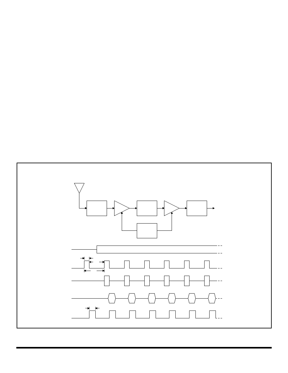
ASH Receiver Block Diagram & Timing Cycle
Antenna
Pulse
Generator
SAW
Delay Line
SAW Filter
RFA1
RFA2
Data
Out
Detector &
Low-Pass
Filter
RF Data Pulse
P1
P2
RFA1 Out
RF Input
P1
Delay Line
Out
P2
t
PW2
t
PW1
t
PRI
t
PRC
Figure 1
ASH Receiver Theory of Operation
Introduction
RFM's RX6500 series amplifier-sequenced hybrid (ASH) receivers are
specifically designed for short-range wireless control and data communica-
tion applications. The receivers provide robust operation, very small size,
low power consumption and low implementation cost. All critical RF func-
tions are contained in the hybrid, simplifying and speeding design-in. The
ASH receiver can be readily configured to support a wide range of data
rates and protocol requirements. The receiver features virtually no RF
emissions, making it easy to certify to short-range (unlicensed) radio regu-
lations.
Amplifier-Sequenced Receiver Operation
The ASH receiver's unique feature set is made possible by its system ar-
chitecture. The heart of the receiver is the amplifier- sequenced receiver
section, which provides more than 100 dB of stable RF and detector gain
without any special shielding or decoupling provisions. Stability is achieved
by distributing the total RF gain over
time. This is in contrast to a superhet-
erodyne receiver, which achieves stability by distributing total RF gain over
multiple frequencies.
Figure 1 shows the basic block diagram and timing cycle for an amplifier-
sequenced receiver. Note that the bias to RF amplifiers RFA1 and RFA2
are independently controlled by a pulse generator, and that the two ampli-
fiers are coupled by a surface acoustic wave (SAW) delay line, which has
a typical delay of 0.5 µs.
An incoming RF signal is first filtered by a narrow-band SAW filter, and is
then applied to RFA1. The pulse generator turns RFA1 ON for 0.5 µs. The
amplified signal from RFA1 emerges from the SAW delay line at the input
to RFA2. RFA1 is now switched OFF and RFA2 is switched ON for 0.55 µs,
amplifying the RF signal further. The ON time for RFA2 is usually set at 1.1
times the ON time for RFA1, as the filtering effect of the SAW delay line
stretches the signal pulse from RFA1 somewhat. As shown in the timing di-
agram, RFA1 and RFA2 are never on at the same time, assuring excellent
receiver stability. Note that the narrow-band SAW filter eliminates sampling
sideband responses outside of the receiver passband, and the SAW filter
and delay line act together to provide very high receiver ultimate rejection.
Amplifier-sequenced receiver operation has several interesting character-
istics that can be exploited in system design. The RF amplifiers in an am-
plifier-sequenced receiver can be turned on and off almost instantly,
allowing for very quick power-down (sleep) and wake-up times. Also, both
RF amplifiers can be off between ON sequences to trade-off receiver noise
figure for lower average current consumption. The effect on noise figure
can be modeled as if RFA1 is on continuously, with an attenuator placed in
front of it with a loss equivalent to 10*log
10
(RFA1 duty factor), where the
duty factor is the average amount of time RFA1 is ON (up to 50%). Since
an amplifier-sequenced receiver is inherently a sampling receiver, the
overall cycle time between the start of one RFA1 ON sequence and the
start of the next RFA1 ON sequence should be set to sample the narrowest
RF data pulse at least 10 times. Otherwise, significant edge jitter will be
added to the detected data pulse.

RF Monolithics, Inc.
Phone: (972) 233-2903
Fax: (972) 387-8148
E-mail: info@rfm.com Page 5 of 10
RFM Europe
Phone: 44 1963 251383
Fax: 44 1963 251510
http://www.rfm.com
©1999 by RF Monolithics, Inc. The stylized RFM logo are registered trademarks of RF Monolithics, Inc.
RX6501-062905
Figure 2
RX6500 Series ASH Receiver Block Diagram
Figure 2 is the general block diagram of the RX6500 series ASH receiver.
Please refer to Figure 2 for the following discussions.
Antenna Port
The only external RF components needed for the receiver are the antenna
and its matching components. Antennas presenting an impedance in the
range of 35 to 72 ohms resistive can be satisfactorily matched to the RFIO
pin with a series matching coil and a shunt matching/ESD protection coil.
Other antenna impedances can be matched using two or three compo-
nents. For some impedances, two inductors and a capacitor will be re-
quired. A DC path from RFIO to ground is required for ESD protection.
Receiver Chain
The output of the SAW filter drives amplifier RFA1. The output of RFA1
drives the SAW delay line, which has a nominal delay of 0.5 µs.
The second amplifier, RFA2, provides 51 dB of gain below saturation. The
output of RFA2 drives a full-wave detector with 19 dB of threshold gain. The
onset of saturation in each section of RFA2 is detected and summed to pro-
vide a logarithmic response. This is added to the output of the full-wave de-
tector to produce an overall detector response that is square law for low
signal levels, and transitions into a log response for high signal levels. This
combination provides excellent threshold sensitivity and more than 70 dB
of detector dynamic range. In combination with the 30 dB of AGC range in
RFA1, more than 100 dB of receiver dynamic range is achieved.
The detector output drives a gyrator filter. The filter provides a three-pole,
0.05 degree equiripple low-pass response with excellent group delay flat-
ness and minimal pulse ringing. The 3 dB bandwidth of the filter can be set
from 4.5 kHz to 1.8 MHz with an external resistor.
The filter is followed by a base-band amplifier which boosts the detected
signal to the BBOUT pin. When the receiver RF amplifiers are operating at
a 50%-50% duty cycle, the BBOUT signal changes about 10 mV/dB, with
a peak-to-peak signal level of up to 685 mV. For lower duty cycles, the mV/
dB slope and peak-to-peak signal level are proportionately less. The de-
tected signal is riding on a 1.1 Vdc level that varies somewhat with supply
voltage, temperature, etc. BBOUT is coupled to the CMPIN pin or to an ex-
ternal data recovery process (DSP, etc.) by a series capacitor. The correct
value of the series capacitor depends on data rate, data run length, and
other factors as discussed in the
ASH Transceiver Designer's Guide.
When the receiver is placed in the power-down (sleep) mode, the output
impedance of BBOUT becomes very high. This feature helps preserve the
charge on the coupling capacitor to minimize data slicer stabilization time
when the receiver switches out of the sleep mode.
Data Slicers
The CMPIN pin drives data slicer DS1, which convert the analog signal
from BBOUT back into a digital stream. Data slicer DS1 is a capacitively-
coupled comparator with provisions for an adjustable threshold. The
threshold, or squelch, offsets the comparator's slicing level from 0 to 90
mV, and is set with a resistor between the RREF and THLD1 pins. This
threshold allows a trade-off between receiver sensitivity and output noise
density in the no-signal condition. For best sensitivity, the threshold is set
to 0. In this case, noise is output continuously when no signal is present.
This, in turn, requires the circuit being driven by the RXDATA pin to be able
to process noise (and signals) continuously.
This can be a problem if RXDATA is driving a circuit that must "sleep" when
data is not present to conserve power, or when it its necessary to minimize
false interrupts to a multitasking processor. In this case, noise can be great-
ly reduced by increasing the threshold level, but at the expense of sensitiv-
ity. The best 3 dB bandwidth for the low-pass filter is also affected by the
threshold level setting of DS1. The bandwidth must be increased as the
threshold is increased to minimize data pulse-width variations with signal
amplitude.
RX6501 ASH Receiver Block Diagram
RFA1
RFA2
SAW
Delay Line
SAW
CR Filter
Log
Antenna
RFIO
ESD
Choke
Detector
Low-Pass
Filter
BB
Pulse Generator
& RF Amp Bias
LPFADJ
PRATE
PWIDTH
RXDATA
CN TRL1
CN TRL0
R
REF
THLD1
Bias Control
Power
Down
Control
Threshold
Control
BBOUT
DS1
Ref
Thld
C
BBO
R
LPF
R
PR
R
PW
R
TH1
20
17
18
14
15
9
5
6
13
VCC1: Pin 2
VCC2: Pin 16
GND1: Pin 1
GND2: Pin 10
GND3: Pin 19
NC: Pin 8
RREF: Pin 11
CMPIN: Pin 6
NC: Pin 4
NC: Pin 12
RFA1
3
7
11 RREF