¸
2-109
2
PO
W
E
R
A
M
P
LI
FI
E
R
S
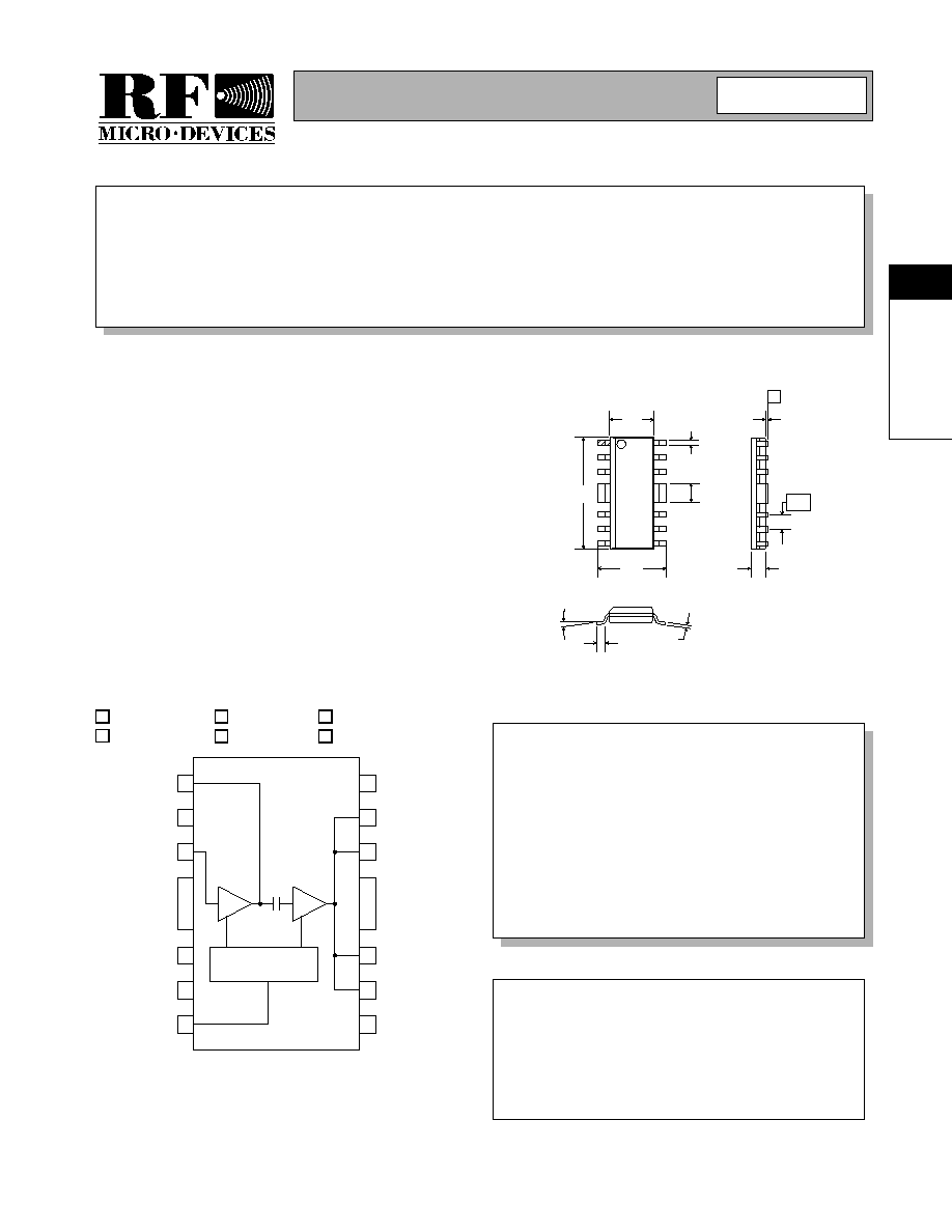
Product Description
Ordering Information
Typical Applications
Features
Functional Block Diagram
RF Micro Devices, Inc.
7628 Thorndike Road
Greensboro, NC 27409, USA
Tel (336) 664 1233
Fax (336) 664 0454
http://www.rfmd.com
Optimum Technology MatchingÆ Applied
Si BJT
GaAs MESFET
GaAs HBT
Si Bi-CMOS
SiGe HBT
Si CMOS
BIAS
1
2
3
4
5
6
7
8
16
15
14
13
12
11
10
9
VCC
NC
RF IN
GND
GND
GND
GND
PC
GND
RF OUT
RF OUT
GND
GND
RF OUT
RF OUT
GND
RF2132
LINEAR POWER AMPLIFIER
∑ 4.8V AMPS Cellular Handsets
∑ 4.8V CDMA/AMPS Handsets
∑ 4.8V JCDMA/TACS Handsets
∑ Driver Amplifier in Cellular Base Stations
∑ Portable Battery-Powered Equipment
The RF2132 is a high power, high efficiency linear ampli-
fier IC. The device is manufactured on an advanced Gal-
lium Arsenide Heterojunction Bipolar Transistor (HBT)
process, and has been designed for use as the final RF
amplifier in dual-mode 4-cell CDMA/AMPS handheld digi-
tal cellular equipment, spread-spectrum systems, and
other applications in the 800MHz to 950MHz band. The
device is self-contained with 50
input and the output
can be easily matched to obtain optimum power, effi-
ciency, and linearity characteristics over varying supply
and control voltages.
∑ Single 4.2V to 5.0V Supply
∑ Up to 29 dBm Linear Output Power
∑ 29dB Gain With Analog Gain Control
∑ 45% Linear Efficiency
∑ On-board Power Down Mode
∑ 800MHz to 950MHz Operation
RF2132
Linear Power Amplifier
RF2132 PCBA
Fully Assembled Evaluation Board
2
Rev B9 010417
0.035
0.016
0.010
0.008
8∞ MAX
0∞ MIN
0.021
0.014
0.392
0.386
0.158
0.150
0.244
0.230
0.069
0.064
0.050
0.060
0.054
-A-
0.009
0.004
Package Style: Standard Batwing

2-110
RF2132
Rev B9 010417
2
PO
W
E
R
A
M
P
LI
FI
E
R
S
Absolute Maximum Ratings
Parameter
Rating
Unit
Supply Voltage (No RF)
-0.5 to +8.0
V
DC
Supply Voltage (P
OUT
<32dBm)
-0.5 to +5.0
V
DC
Power Control Voltage (V
PC
)
-0.5 to +5.0 or V
CC
V
DC Supply Current
800
mA
Input RF Power
+12
dBm
Output Load VSWR
10:1
Storage Temperature
-40 to +150
∞C
Junction Temperature
200
∞C
Parameter
Specification
Unit
Condition
Min.
Typ.
Max.
Overall
T = 25 ∞C, V
CC
= 4.8V, V
PC
= 4.0V,
Freq= 824MHz to 849MHz
Usable Frequency Range
800
824 to 849
950
MHz
Linear Gain
27
29
31
dB
Total Linear Efficiency
40
45
%
Efficiency at Max Output
50
55
%
OFF Isolation
23
27
dB
V
PC
=0V,P
IN
=+6dBm
Second Harmonic
-30
dBc
Including Second Harmonic Trap
Maximum Linear Output Power
28.5
29
IS-95A CDMA Modulation
Adjacent Channel Power Rejec-
tion @ 885 kHz
-46
-44
dBc
Pout = 28 dBm
ACPR can be improved by trading off effi-
ciency.
Adjacent Channel Power Rejec-
tion @ 1.98 MHz
-58
-56
dBc
Pout = 28 dBm
Maximum CW Output Power
31.5
32
dBm
Operating Case Temperature
-30
110
∞C
Pout = 31 dBm, Efficiency = 55%
Ambient Operating Temperature
-30
100
∞C
Junction to Case Thermal Resis-
tance
85
∞C/W
Input VSWR
<2:1
Output Load VSWR
10:1
No oscillations
Power Down
Turn On/Off Time
100
ns
Total Current
10
µ
A
"OFF" State
V
PC
"OFF" Voltage
0.2
0.5
V
V
PC
"ON" Voltage
3.6
4.0
Vcc
V
Power Supply
Power Supply Voltage
4.2
4.8
5.0
V
Operating voltage
Idle Current
40
100
mA
V
PC
= 4.0V
Current into VPC pin
15
20
mA
"ON" State
Caution! ESD sensitive device.
RF Micro Devices believes the furnished information is correct and accurate
at the time of this printing. However, RF Micro Devices reserves the right to
make changes to its products without notice. RF Micro Devices does not
assume responsibility for the use of the described product(s).
2-111
RF2132
Rev B9 010417
2
PO
W
E
R
A
M
P
LI
FI
E
R
S
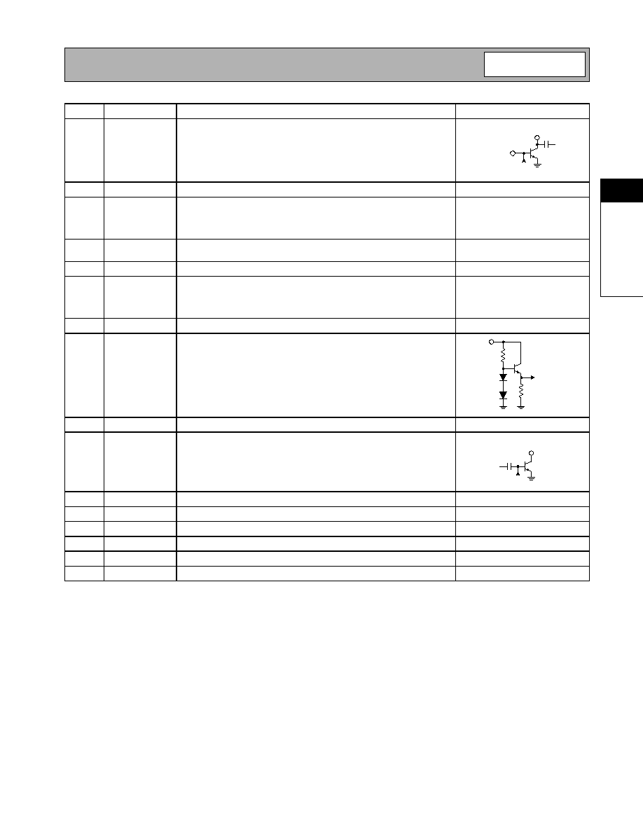
Pin
Function
Description
Interface Schematic
1
VCC1
Power supply for the driver stage, and interstage matching. Shunt
inductance is required on this pin, which can be achieved by an induc-
tor to V
CC
, with a decoupling capacitor on the V
CC
side. The value of
the inductor is frequency dependent; 3.3nH is required for 830MHz,
and 1.2nH for 950MHz. Instead of an inductor, a high impedance
microstrip line can be used.
2
NC
Not Connected.
3
RF IN
RF input. This is a 50
input, but the actual input impedance depends
on the interstage matching network connected to pin 1. An external DC
blocking capacitor is required if this port is connected to a DC path to
ground or a DC voltage.
See pin 1.
4
GND
Ground connection. Keep traces physically short and connect immedi-
ately to the ground plane for best performance.
5
GND
Same as pin 4.
6
GND
Ground for stage 1. Keep traces physically short and connect immedi-
ately to ground plane for best performance. This ground should be iso-
lated from the batwing and other ground contacts. See evaluation
board layout.
7
GND
Same as pin 6.
8
PC
Power Control. When this pin is "low", all circuits are shut off. A "low" is
typically 0.5V or less at room temperature. During normal operation
this pin is the power control. Control range varies from about 2V for
0dBm to V
CC
for +31dBm RF output power. The maximum power that
can be achieved depends on the actual output matching. PC should
never exceed 5.0V or V
CC
, whichever is the lowest.
9
GND
Same as pin 4.
10
RF OUT
RF Output and power supply for the output stage. The four output pins
are combined, and bias voltage for the final stage is provided through
these pins. The external path must be kept symmetric until combined to
ensure stability. An external matching network is required to provide the
optimum load impedance; see the application schematics for details.
11
RF OUT
Same as pin 10.
See pin 10.
12
GND
Same as pin 4.
13
GND
Same as pin 4.
14
RF OUT
Same as pin 10.
See pin 10.
15
RF OUT
Same as pin 10.
See pin 10.
16
GND
Same as pin 4.
RF IN
VCC
From Bias
Stages
PC
To RF
Transistors
RF OUT
From Bias
Stages

2-112
RF2132
Rev B9 010417
2
PO
W
E
R
A
M
P
LI
FI
E
R
S
Application Schematic
Evaluation Board Schematic
(Download Bill of Materials from www.rfmd.com.)
1
2
3
4
5
6
7
8
16
15
14
13
12
11
10
9
BIAS
1.8 nH
100 pF
18 k
100 pF
RF IN
V
PC
1 nF
1 nF
100 pF
6.8 nH
3 pF
V
CC
12 pF
3.3 nH
4.3 pF
100 pF
RF OUT
Vcc = 4.8 V
Vpc = 4.0 V
BIAS
1
2
3
4
5
6
7
8
16
15
14
13
12
11
10
9
L1
1.8 nH
C6
100 pF
R1
18 k
C14
100 pF
C13
1 nF
C12
3.3
µ
F
P1-3
C8
33 pF
J1
L3
3.3 nH
C11
4.3 pF
C9
100 pF
J2
C7
3 pF
L2
6.8 nH
C4
1 nF
C1
100 nF
C2
11
µ
F
C3
1
µ
F
C10
12 pF
P1-1
C5
100 pF
RF IN
RF OUT
P1-1
P1-3
P1
PC
GND
VCC
1
2
3
Vcc = 4.8 V
Vpc = 4.0 V
Power supply filtering/bypassing for V
cc
Power supply filtering/bypassing for V
PC
Adds bias to the first
amplifier stage for
improved linearity
Bias inductor for the
amplifier output stage
Harmonic trap: C7 series resonates with
internal bondwires of pins 14 and 15 at
2f
0
to effectively short out 2nd harmonic
for optimum gain and efficiency
Matching network for
optimum load impedance
Interstage tuning (L1) for
centering output frequency

2-113
RF2132
Rev B9 010417
2
PO
W
E
R
A
M
P
LI
FI
E
R
S
Evaluation Board Layout
2" x 2"

2-114
RF2132
Rev B9 010417
2
PO
W
E
R
A
M
P
LI
FI
E
R
S
RF2132 Evaluation Board
Vcc = 4.8 V, Vpc = 4.0 V, Frequency = 836 MHz, IS-95A CDMA
0
10
20
30
40
50
60
70
80
90
28
26
24
22
20
18
16
14
12
10
Pout (dBm)
ACPR
(-d
Bc),
Effi
ci
en
cy
(%
)
0
50
100
150
200
250
300
350
Curre
nt
(m
A)
ACPR 885 kHz
ACPR 1.98 MHz
Current
Total Efficiency