 | –≠–ª–µ–∫—Ç—Ä–æ–Ω–Ω—ã–π –∫–æ–º–ø–æ–Ω–µ–Ω—Ç: RF2196 | –°–∫–∞—á–∞—Ç—å:  PDF PDF  ZIP ZIP |

¸
2-203
2
PO
W
E
R
A
M
P
LI
FI
E
R
S
Preliminary
Product Description
Ordering Information
Typical Applications
Features
Functional Block Diagram
RF Micro Devices, Inc.
7625 Thorndike Road
Greensboro, NC 27409, USA
Tel (336) 664 1233
Fax (336) 664 0454
http://www.rfmd.com
Optimum Technology MatchingÆ Applied
Si BJT
GaAs MESFET
GaAs HBT
Si Bi-CMOS
SiGe HBT
Si CMOS
4
VPD2
3
MODE
2
VPD1
13
NC
14
NC
15
NC
16
RF
IN
1
GN
D
10 VCC
11 VCC1
12 VCC1
5
GN
D
6
7
RF
O
U
T
8
RF
O
U
T
9
GN
D
NC
RF2196
3V PCS LINEAR POWER AMPLIFIER
∑ 3V CDMA PCS Handsets
∑ 3V CDMA KPCS Handsets
∑ 3V TDMA/GAIT PCS Handsets
∑ 3 V CDMA 2000 PCS Handsets
∑ Spread-Spectrum Systems
∑ Portable Battery-Powered Equipment
The RF2196 is a high-power, high-efficiency linear ampli-
fier IC targeting 3V handheld systems. The device is
manufactured on an advanced Gallium Arsenide process,
and has been designed for use as the final RF amplifier in
3 V CDMA and CDMA2000 handsets as well as other
applications in the 1750MHz to 1910MHz band. The
RF2196 has a low power mode to extend battery life
under low output power conditions. The package is an
ultra small 4mmx4mm leadless plastic package with
backside ground.
∑ Single 3V Supply
∑ 29dBm Linear Output Power
∑ 35% Linear Efficiency
∑ Low Power Mode (Up to 20dBm)
∑ 55mA Idle Current
RF2196
3V PCS LINEAR Power Amplifier
RF2196 PCBA
Fully Assembled Evaluation Board
2
Rev A0 010518
3.75
3.75
+
1.50 SQ
4.00
4.00
1
0.45
0.28
3.20
1.60
0.75
0.50
12∞
INDEX AREA 3
1.00
0.90
0.75
0.65
0.05
0.00
NOTES:
5
Package Warpage: 0.05 max.
4
Pins 1 and 9 are fused.
Shaded Pin is Lead 1.
1
Dimension applies to plated terminal and is measured between
0.10 mm and 0.25 mm from terminal tip.
2
The terminal #1 identifier and terminal numbering convention
shall conform to JESD 95-1 SPP-012. Details of terminal #1
identifier are optional, but must be located within the zone
indicated. The identifier may be either a mold or marked
feature.
3
0.80
TYP
2
1
Dimensions in mm.
Package Style: LCC, 16-Pin, 4x4
Preliminary
2-204
RF2196
Rev A0 010518
2
PO
W
E
R
A
M
P
LI
FI
E
R
S
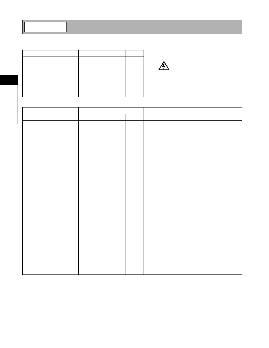
Absolute Maximum Ratings
Parameter
Rating
Unit
Supply Voltage (RF off)
+8.0
V
DC
Supply Voltage (P
OUT
31dBm)
+5.2
V
DC
Mode Voltage (V
MODE
)
+4.2
V
DC
Control Voltage (V
REG
)
+3.0
V
DC
Input RF Power
+10
dBm
Operating Case Temperature
-30 to +110
∞C
Storage Temperature
-30 to +150
∞C
Moisture Sensitivity
Modified JEDEC Level 2
Parameter
Specification
Unit
Condition
Min.
Typ.
Max.
High Power State
(V
MODE
Low)
Case T= 25∞C, V
CC
= 3.4V, V
REG
=2.85V,
V
MODE
= 0V to 0.5V, Freq= 1850MHz to
1910MHz (unless otherwise specified)
Frequency Range
1850
1910
MHz
Linear Gain
25
27
dB
Second Harmonic
-50
dBc
Third Harmonic
-63
dBc
Maximum Linear Output Power
(CDMA Modulation)
29
dBm
Total Linear Efficiency
35
%
P
OUT
=29dBm
Adjacent Channel Power Rejec-
tion
-46
-44
dBc
ACPR @1.25MHz
-62
-56
dBc
ACPR @2.25MHz
Input VSWR
<2:1
Output VSWR
10:1
No damage.
6:1
No oscillations. > -70dBc
Noise Power
-141
dBm/Hz
At 80MHz offset.
Low Power State
(V
MODE
High)
Case T= 25∞C, V
CC
= 3.4V, V
REG
=2.85V,
V
MODE
= 2V to 3V, Freq= 1850MHz to
1910MHz (unless otherwise specified)
Frequency Range
1850
1910
MHz
Linear Gain
16
20
dB
Second Harmonic
-45
dBc
Third Harmonic
-60
dBc
Maximum Linear Output Power
(CDMA Modulation)
16
20
dBm
Max I
CC
160
mA
P
OUT
=+16dBm (all currents included)
Adjacent Channel Power Rejec-
tion
< -50
-46
dBc
ACPR @1.25MHz
< -60
-58
dBc
ACPR @2.25MHz
Input VSWR
2:1
Output VSWR
10:1
No damage.
6:1
No oscillations. > -70dBc
Caution! ESD sensitive device.
RF Micro Devices believes the furnished information is correct and accurate
at the time of this printing. However, RF Micro Devices reserves the right to
make changes to its products without notice. RF Micro Devices does not
assume responsibility for the use of the described product(s).

Preliminary
2-205
RF2196
Rev A0 010518
2
PO
W
E
R
A
M
P
LI
FI
E
R
S
Parameter
Specification
Unit
Condition
Min.
Typ.
Max.
High Power State CDMA
2000 1x (V
MODE
LOW)
Case T = 25∞C, V
CC
= 3.4V, V
REG
=2.85V,
V
MODE
= 0V to 0.5V, Freq=1850MHz to
1910MHz (unless otherwise specified)
Frequency Range
1850
1910
MHz
Linear Gain
27
dB
Pilot+ DCCH 9600
Maximum Linear Output Power
(CDMA 2000 Modulation)
26.5
dBm
2.5dB Backoff included in IS95D 5.4dB peak
to average at CCDF of 1%
Adjacent Channel Power Rejec-
tion
-49
dBc
ACPR@ 1.25MHz
-61
dBc
ACPR@ 2.25MHz
Pilot+ FCH 9600+ SCH0 9600
Maximum Linear Output Power
(CDMA 2000 Modulation)
29
dBm
4.5dB peak to average at CCDF of 1%
Adjacent Channel Power Rejec-
tion
-46
dBc
ACPR@ 1.25MHz
-63
dBc
ACPR@ 2.25MHz
Low Power State CDMA
2000 1x (V
MODE
HIGH)
Case T = 25∞C, V
CC
= 3.4V, V
REG
=2.85V,
V
MODE
=2V to 3V, Freq=1850MHz to
1910MHz
Frequency Range
1850
1910
MHz
Linear Gain
19
dB
Pilot+ DCCH 9600
Maximum Linear Output Power
(CDMA 2000 Modulation)
16
20
dBm
5.4dB peak to average at CCDF of 1%
Adjacent Channel Power Rejec-
tion
-52
dBc
ACPR@ 1.25MHz
-65
dBc
ACPR@ 2.25MHz
Pilot+ FCH 9600+SCHO 9600
Maximum Linear Output Power
(CDMA 2000 Modulation)
16
20
dBm
4.5dB peak to average at CCDF of 1%
Adjacent Channel Power Rejec-
tion
-52
dBc
ACPR@ 1.25MHz
-65
dBc
ACPR@ 2.25MHz
DC Supply
Supply Voltage
3.0
3.4
4.2
V
Quiescent Current
185
mA
V
MODE
= Low
55
mA
V
MODE
= High
V
REG
Current
5
10
mA
V
MODE
Current
1
mA
Total Current (Power Down)
10
µ
A
V
REG
= Low
V
REG
"Low" Voltage
0
0.5
V
V
REG
"High" Voltage
2.75
2.85
2.95
V
V
MODE
"Low" Voltage
0
0.5
V
V
MODE
"High" Voltage
2.0
3.0
V
Preliminary
2-206
RF2196
Rev A0 010518
2
PO
W
E
R
A
M
P
LI
FI
E
R
S
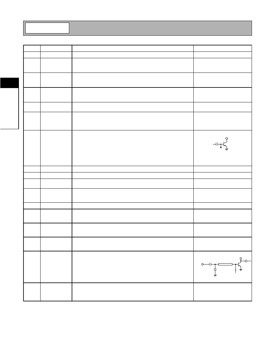
Pin
Function
Description
Interface Schematic
1
GND
This pin is internally grounded to the die flag.
2
VREG1
Power Down control for first stage. Regulated voltage supply for ampli-
fier bias. In Power Down mode, both V
REG
and V
MODE
need to be LOW
(<0.5V).
3
MODE
For nominal operation (High Gain Mode), V
MODE
is set LOW. When set
HIGH, the driver and final are dynamically scaled to reduce the device
size and as a result to reduce idle current.
4
VREG2
Power Down control for the second stage. Regulated voltage supply for
amplifier bias. In Power Down mode, both V
REG
and V
MODE
need to be
LOW (<0.5V).
5
GND
Connect to ground plane via 15nH inductor. DC return for the second
stage bias circuit.
6
NC
This pin has no internal bonding; therefore, this pin can be connected
to output pin 7, connected to the ground plane, or not connected. Slight
tuning of the output match may be required due to stray capacitance of
the pin.
7
RF OUT
RF output and power supply for final stage. This is the unmatched col-
lector output of the second stage. A DC block is required following the
matching components. The biasing may be provided via a parallel L-C
set for resonance at the operating frequency of 1710MHz to 1910MHz.
It is important to select an inductor with very low DC resistance with a
1A current rating. Alternatively, shunt microstrip techniques are also
applicable and provide very low DC resistance. Low frequency bypass-
ing is required for stability.
8
RF OUT
Same as pin 7.
See pin 7.
9
GND
This pin is internally grounded to the die flag.
10
VCC
Supply for bias reference and control circuits. High frequency bypass-
ing may be necessary.
11
VCC1
Power supply for first stage and interstage match. Pins 11 and 12
should be connected by a common trace where the pins contact the
printed circuit board.
12
VCC1
Same as pin 11.
13
NC
It is recommended that these pins be connected to the ground plane for
improved isolation between RF IN (pin 16) and the VCC1 pins (pins 11
and 12).
14
NC
It is recommended that these pins be connected to the ground plane for
improved isolation between RF IN (pin 16) and the VCC1 pins (pins 11
and 12).
15
NC
It is recommended that these pins be connected to the ground plane for
improved isolation between RF IN (pin 16) and the VCC1 pins (pins 11
and 12).
16
RF IN
RF input. An external 15pF series capacitor is required as a DC block.
In addition, the matching circuit shown is required to improve input
VSWR.
Pkg
Base
GND
Ground connection. The backside of the package should be soldered to
a top side ground pad which is connected to the ground plane with mul-
tiple vias. The pad should have a short thermal path to the ground
plane.
RF OUT
From Bias
Network
VCC1
15 pF
RF IN
From
Bias
Stages
GND1
3.6 pF
TL

Preliminary
2-207
RF2196
Rev A0 010518
2
PO
W
E
R
A
M
P
LI
FI
E
R
S
Application Schematic
US - CDMA
15
16
1
2
3
4
12
11
10
9
8
7
6
5
14
13
3.6 pF
15 pF
RF IN
4.7 pF
2.2 pF
15 pF
RF OUT
2.5 nH
2.2 pF
15 pF
10 nF
Pins 1 and 9 are internally grounded to the die flag.
TL
1
TL
2
15 pF
Jumper
VREG
1 k
VMODE
12 nH
15 pF
Jumper
15 pF
VCC
11 pF
Ferrite
10
Bypassing for
V
REG1
and V
REG2
Bias return
Matching network for
optimum load impedance
Interstage tuning for centering
frequency response
RF Choke - Bias inductor
for the amplifier interstage
TL
3
Matching network for
optimum input return loss
4.7
µ
F
Bypassing for V
CC
1
µ
F
+
10 nF
1
µ
F
+
TL4
CDMA (US)
Transmission
Line Length
15 mils
TL
3
200 mils
TL
4
140 mils
TL
2
30 mils
TL
1

Preliminary
2-208
RF2196
Rev A0 010518
2
PO
W
E
R
A
M
P
LI
FI
E
R
S
Evaluation Board Schematic
US - CDMA
15
16
1
2
3
4
12
11
10
9
8
7
6
5
14
13
C24
3.6 pF
C5
15 pF
RF IN
C1**
4.7 pF
C14**
2.2 pF
C3
15 pF
RF OUT
L1*
2.5 nH
C7
2.2 pF
C4
15 pF
C28
10 nF
* L1 is a High Q inductor (i.e., Coilcraft 0805HQ-series).
**C1 and C14 are High Q capacitors
(i.e., Johanson C-series).
Pins 1 and 9 are internally grounded to the die flag.
TL
1
TL
2
C27
15 pF
R12
Jumper
P2
R1
1 k
P3
L4
12 nH
C13
15 pF
R11
Jumper
C6
15 pF
P1
C30
11 pF
L2
Ferrite
10
C8
10 nF
TL
3
C2
4.7 uF
Transmission
Line Length
CDMA (US)
TL
3
15 mils
TL
2
140 mils
TL
1
30 mils
P3
VMODE
P1
1
P1
VCC
P1
1
P2
VREG
P1
1
P4
GND
P1
1
C26
1 uF +
C25
1 uF
+
TL4
CDMA (US)
Board
C30 (pF)
11
C1 (pF)
4.7
L1 (nH)
2.5
C14 (pF)
2.2
TL
4
200 mils

Preliminary
2-209
RF2196
Rev A0 010518
2
PO
W
E
R
A
M
P
LI
FI
E
R
S
Evaluation Board Layout
Board Size 2.0" x 2.0"
Board Thickness 0.028"; Board Material FR-4; Multi-Layer; Ground Plane at 0.014"

Preliminary
2-210
RF2196
Rev A0 010518
2
PO
W
E
R
A
M
P
LI
FI
E
R
S