4-221
4
GEN
E
RA
L
P
URPO
S
E
A
M
P
L
IF
IE
RS
Preliminary
Product Description
Ordering Information
Typical Applications
Features
Functional Block Diagram
RF Micro Devices, Inc.
7625 Thorndike Road
Greensboro, NC 27409, USA
Tel (336) 664 1233
Fax (336) 664 0454
http://www.rfmd.com
Optimum Technology Matching� Applied
Si BJT
GaAs MESFET
GaAs HBT
Si Bi-CMOS
�
SiGe HBT
Si CMOS
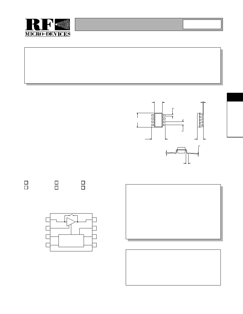
8
7
6
5
RF OUT
ISET
VCC
ENABLE
RF IN
GND1
GND2
IPSET
1
2
3
4
Bias Circuits
RF2371
3V LOW NOISE AMPLIFIER
� GSM Handsets
� CDMA Handsets
� TDMA Handsets
� IF or RF Buffer Amplifiers
� Driver Stage for Power Amplifiers
� Oscillator Loop Amplifiers
The RF2371 is a general purpose, low-cost, high perfor-
mance low noise amplifier designed for operation from a
2.7V to 4V supply with low current consumption. The
attenuation of the device is controlled when in power
down mode, providing a known gain step. The RF2371 is
available in a small industry-standard SOT23-8 surface
mount package, enabling compact designs which con-
serve board space. The design features a highly accurate
PTAT (Proportional To Absolute Temperature) biasing
scheme using bandgap cells.
� 700MHz to 2000MHz Operation
� 2.7V to 3.6V Single Supply
� +5dBm Input IP
3
at 3.0mA
� 12dB Gain at 1950MHz
� 1.8dB Noise Figure at 1950MHz
� 17dB Gain Step
RF2371
3V Low Noise Amplifier
RF2371 PCBA
Fully Assembled Evaluation Board
4
Rev A2 010205
0.127
3�MAX
0�MIN
0.55
0.35
0.365
1.59
1.61
3.00
2.60
3.00
2.80
0.650
0.15
0.05
1.44
1.04
TEXT*
*When Pin 1 is in
upper left, text
reads downward
(as shown).
Package Style: SOT23-8

Preliminary
4-222
RF2371
Rev A2 010205
4
GEN
E
RA
L
P
URPO
S
E
A
M
P
L
IF
IE
RS
Absolute Maximum Ratings
Parameter
Rating
Unit
Supply Voltage
4.0
V
Supply Current
20
mA
Operating Ambient Temperature
-40 to +85
�C
Storage Temperature
-40 to +150
�C
Parameter
Specification
Unit
Condition
Min.
Typ.
Max.
Overall
T = 27� C, V
CC
= 2.7V, V
ISELECT
=0V,
V
ENABLE
= 2.7V
Frequency Range
700 to 2000
MHz
LNA Performance
Freq= 1.95GHz
Gain
10.5
12.5
dB
Noise Figure
1.6
dB
Input IP3
+4
+6
dBm
At 2.9mA
Input P1dB
-14
dBm
Input VSWR
5:1
dB
(Noise match)
Output VSWR
1.5:1
dB
Off Mode Gain
-5.0
dB
V
ENABLE
=0V
Gain
17
dB
Freq= 836MHz
Noise Figure
1.6
dB
Input IP3
0
dBm
Current Control
Internal Current Setting "ON"
CMOS Low
V
Voltage on ISELECT
External Current Setting "ON"
CMOS High
V
Voltage on ISELECT
Current into ISELECT
1
�
A
V
ISELECT
=2.7V
Power Control
Power "ON" Voltage
CMOS High
V
Voltage on ENABLE
Power "OFF" Voltage
CMOS Low
V
Voltage on ENABLE
Current into ENABLE
1
�
A
V
ENABLE
=2.7V
Power Supply
Operating Voltage
2.7 to 3.6
V
Operating Current
2.9
5
mA
V
CC
= 2.7V, Internal current setting
Leakage Current
1
�
A
V
ENABLE
=0V
Caution! ESD sensitive device.
RF Micro Devices believes the furnished information is correct and accurate
at the time of this printing. However, RF Micro Devices reserves the right to
make changes to its products without notice. RF Micro Devices does not
assume responsibility for the use of the described product(s).

Preliminary
4-223
RF2371
Rev A2 010205
4
GEN
E
RA
L
P
URPO
S
E
A
M
P
L
IF
IE
RS
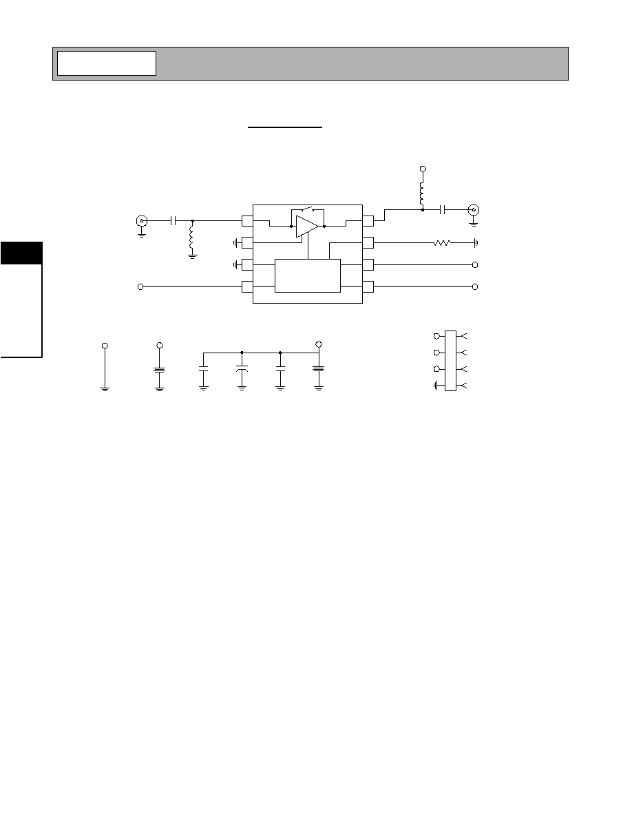
Pin
Function
Description
Interface Schematic
1
RF IN
RF input pin. This pin is not internally DC blocked and requires an
external blocking capacitor.
2
GND1
Ground connection for the LNA. Keep traces physically short and con-
nect immediately to ground plane for best performance.
3
GND2
Ground connection for the bias circuits.
4
IPSET
This pin selects the internal current setting when CMOS level "low", and
the external current setting when this pin is CMOS level "high".
5
ENABLE
Power down control. This is a CMOS input. When this pin is CMOS
"high" the device is enabled. When the level is CMOS "low" the device
is shut off and a controlled attenuator is turned on.
6
VCC
Power supply for the bias circuits.
7
ISET
This pin sets the current for the device.
8
RF OUT
RF output pin. Bias for the LNA is provided through this pin, hence it
should be connected to VCC through an inductor.

Preliminary
4-224
RF2371
Rev A2 010205
4
GEN
E
RA
L
P
URPO
S
E
A
M
P
L
IF
IE
RS
Application Information
The RF2371 may be configured to use either the internal current setting or the external current setting. This choice is
made by asserting IPSET, pin 4, to CMOS level "low" for the internal current setting or CMOS level "high" for the external
current setting.
Internal Current Setting
When IPSET is set to CMOS "low", the internal current settings are chosen. This current draw is typically 2.9mA. In this
mode, the resistorR1 may be removed from the evaluation board schematic and ISET left floating. The condition for opti-
mal IP3 is to use the internal current setting option and leave the ISET pin open (no connect).
External Current Setting
The external current setting is configured by using the series resistor between ISET, pin7, and ground (refer to resistor
R1 in evaluation board schematic). The value of the resistor may be changed to permit various operating currents up to a
maximum allowable current of 20mA. The table below gives approximate minimum R1 values to allow the 20mA maxi-
mum current draw at various operating voltages.
Note: When the internal current setting was selected, the part tested drew 4.4mA, which is higher than typical
(2.9 mA). Thus values of R1 given vary from part to part.
V
CC
(V)
Resistor R1 (
)
Current Draw (mA)
2.7
2.4k
20.1
3.0
2.7k
20.1
3.3
3.0k
20.0
3.6
3.3k
19.8

Preliminary
4-225
RF2371
Rev A2 010205
4
GEN
E
RA
L
P
URPO
S
E
A
M
P
L
IF
IE
RS
Application Schematic
1.95GHz
Application Schematic
836MHz
8
7
6
5
1
2
3
4
ENABLE
V
CC
1 k
3.3 nH
1.5 pF
V
CC
RF OUT
IPSET
22 nF
RF IN
10 nF
Bias Circuits
8
7
6
5
1
2
3
4
IPSET
22 nF
RF IN
82 nH
ENABLE
V
CC
1 k
18 nH
1 pF
V
CC
RF OUT
Bias Circuits
Preliminary
4-226
RF2371
Rev A2 010205
4
GEN
E
RA
L
P
URPO
S
E
A
M
P
L
IF
IE
RS
Evaluation Board Schematic
(Download Bill of Materials from www.rfmd.com.)
8
7
6
5
1
2
3
4
GND
IPSET
ENABLE
VCC
P1
1
2
3
4
CON4
C5
22 nF
C3
1 nF
C4
1 uF
+
VCC
2.7 V
-
+
VCC
ENVCC
2.6 V
-
+
ENABLE
IPSET
ENABLE
R1
1 k
L1
3.9 nH
C2
1.5 pF
J1
LNA OUTPU
IPSET
C1
22 nF
L2
10 nH
J2
LNA INPUT
VCC
VCC
Bias Circuits
2371400-

Preliminary
4-227
RF2371
Rev A2 010205
4
GEN
E
RA
L
P
URPO
S
E
A
M
P
L
IF
IE
RS
Evaluation Board Layout
Board Size 0.833" x 1.009"
Board Thickness 0.031", Board Material FR-4

Preliminary
4-228
RF2371
Rev A2 010205
4
GEN
E
RA
L
P
URPO
S
E
A
M
P
L
IF
IE
RS