 | –≠–ª–µ–∫—Ç—Ä–æ–Ω–Ω—ã–π –∫–æ–º–ø–æ–Ω–µ–Ω—Ç: RF2421 | –°–∫–∞—á–∞—Ç—å:  PDF PDF  ZIP ZIP |

9-15
9
A
T
T
E
NT
U
A
T
O
R
S
AN
D
SWI
T
CH
ES
Product Description
Ordering Information
Typical Applications
Features
Functional Block Diagram
RF Micro Devices, Inc.
7625 Thorndike Road
Greensboro, NC 27409, USA
Tel (336) 664 1233
Fax (336) 664 0454
http://www.rfmd.com
Optimum Technology MatchingÆ Applied
Si BJT
GaAs MESFET
GaAs HBT
Si Bi-CMOS
!
SiGe HBT
Si CMOS
1
2
3
4
8
7
6
5
NC
RF IN
GND
RF OUT
NC
G10
VDD
NC
RF2421
10dB SWITCHED ATTENUATOR
∑ Power Control in Communication Systems
∑ CMOS Compatible Programmable
Attenuator
∑ Commercial and Consumer Systems
∑ Portable Battery-Powered Equipment
The RF2421 is a monolithic switched attenuator. The
device is built using a Gallium Arsenide process technol-
ogy and has a single step attenuation of 10dB. The input
and output of the device has a low VSWR 50
match.
The RF output can drive up to +16dBm. This unit is
intended for use in systems that require RF power control
by digital means. No negative supply voltages are
required, and the current consumption is less than 5
µ
A
when the attenuator is off.
∑ Single 2.7V to 6V Supply
∑ 10dB Single Step Attenuation
∑ 1 dB Insertion Loss
∑ 1-bit Digitally Controlled Attenuation
∑ Digitally Controlled Power Down Mode
∑ 500MHz to 3000 MHz Operation
RF2421
10dB Switched Attenuator
RF2421 PCBA
Fully Assembled Evaluation Board
9
Rev A6 001102
0.244
0.229
0.157
0.150
0.018
0.014
0.050
0.068
0.053
NOTES:
1. Shaded lead is Pin 1.
2. All dimensions are excluding
mold flash.
3. Lead coplanarity -
0.005 with respect to datum "A".
Dimensions in mm
0.196
0.189
0.008
0.004
-A-
8∞ MAX
0∞ MIN
0.034
0.016
0.009
0.007
Package Style: SOIC-8
9-16
RF2421
Rev A6 001102
9
A
T
T
E
NT
U
A
T
O
R
S
AN
D
SWI
T
CH
ES
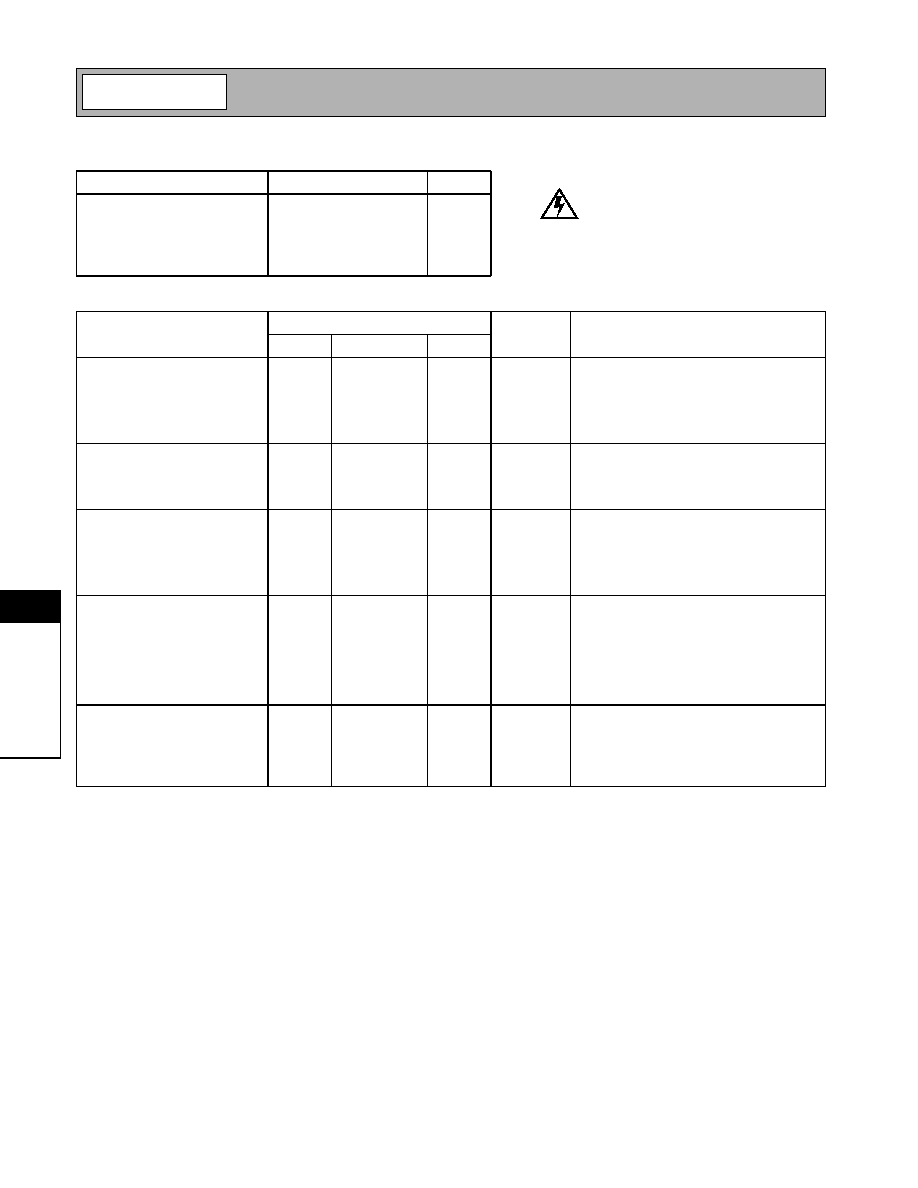
Absolute Maximum Ratings
Parameter
Rating
Unit
Supply Voltage
-0.5 to +6.0
V
DC
Control Voltage
-0.5 to +6.0
V
Input RF Power
+20
dBm
Operating Ambient Temperature
-40 to +85
∞C
Storage Temperature
-40 to +150
∞C
Parameter
Specification
Unit
Condition
Min.
Typ.
Max.
Overall
T = 25 ∞C, V
DD
=5.0V, Freq= 915MHz
Frequency Range
500 to 3000
MHz
Insertion Loss
1.0
1.5
dB
V
G10
=0V
DC
Insertion Loss
9.5
10
10.5
dB
V
G10
= V
DD
Gain Flatness
0.25
dB
In any 50MHz band
Input
Input Impedance
50
Input VSWR
1.3:1
Input 1dB Compression
+17
dBm
Attenuation Control
Attenuation "ON" Voltage
2.5
V
DD
V
Voltage supplied to input
Attenuation "OFF" Voltage
0.3
V
Voltage supplied to input
Current
0.4
0.5
mA
Into control line, V
G10
=5V
DC
Response Time
<10
ns
Output
IM
3
-60
dBc
With 0dBm output in each of 2 tones, attenu-
ation "OFF".
Harmonic Output
-40
dBc
With 0dBm output in each of 2 tones, attenu-
ation "OFF".
Output Impedance
50
Output VSWR
1.3:1
Power Supply
Voltage
5
V
Specifications
2.7
5
6.0
V
Operating Limits
Current
0.5
mA
Attenuation "ON"
5
µ
A
Attenuation "OFF"
Caution! ESD sensitive device.
RF Micro Devices believes the furnished information is correct and accurate
at the time of this printing. However, RF Micro Devices reserves the right to
make changes to its products without notice. RF Micro Devices does not
assume responsibility for the use of the described product(s).

9-17
RF2421
Rev A6 001102
9
A
T
T
E
NT
U
A
T
O
R
S
AN
D
SWI
T
CH
ES
Evaluation Board Schematic
(Download Bill of Materials from www.rfmd.com.)
Pin
Function
Description
Interface Schematic
1
NC
Not internally connected. This pin can be grounded.
2
RF IN
RF Input. This pin is not DC blocked, and an external blocking capacitor
is recommended. The value depends on the frequency used.
3
GND
Ground connection. Keep trace physically short and connect immedi-
ately to the ground plane for best performance.
4
RF OUT
RF Output. This pin is not DC blocked, and an external blocking capac-
itor is recommended. The value depends on the frequency used.
See pin 2.
5
NC
Not internally connected. This pin can be grounded.
6
VDD
Power supply pin. An external RF bypass capacitor is recommended.
7
G10
Control pin for the 10dB attenuator. This pin has an internal pull-down
resistor, so when the pin is not connected the attenuator will be turned
off.
8
NC
Not internally connected. This pin can be grounded.
RF IN
RF OUT
G10
1
2
3
4
8
7
6
5
C1
100 pF
C2
100 nF
P1-1
P1-3
C3
100 pF
C4
100 pF
50
µ
strip
RF IN
J1
RF OUT
J2
50
µ
strip
P1-1
P1-3
P1
ATTN
GND
VDD
1
2
3
2421400 Rev A

9-18
RF2421
Rev A6 001102
9
A
T
T
E
NT
U
A
T
O
R
S
AN
D
SWI
T
CH
ES
Evaluation Board Layout
Board Thickness 0.031"; Board Material FR-4