 | –≠–ª–µ–∫—Ç—Ä–æ–Ω–Ω—ã–π –∫–æ–º–ø–æ–Ω–µ–Ω—Ç: RF2485 | –°–∫–∞—á–∞—Ç—å:  PDF PDF  ZIP ZIP |
5-55
5
M
O
D
U
L
A
T
O
RS
AND
UP
C
O
N
V
E
R
T
E
RS
Preliminary
Product Description
Ordering Information
Typical Applications
Features
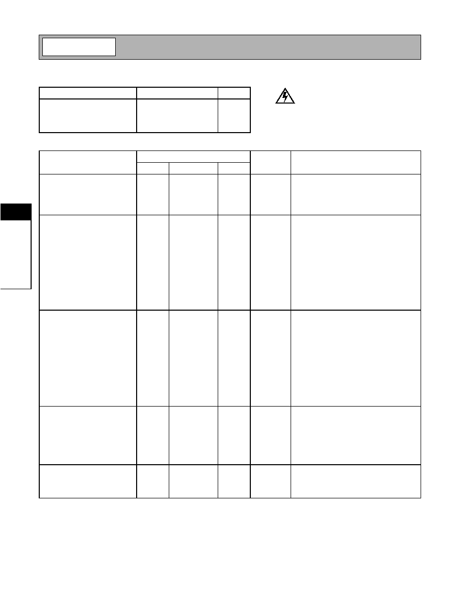
Functional Block Diagram
RF Micro Devices, Inc.
7625 Thorndike Road
Greensboro, NC 27409, USA
Tel (336) 664 1233
Fax (336) 664 0454
http://www.rfmd.com
Optimum Technology MatchingÆ Applied
Si BJT
GaAs MESFET
GaAs HBT
Si Bi-CMOS
¸
SiGe HBT
Si CMOS
1
2
3
4
5
6
7
14
13
12
11
10
9
8
VDD2
VDD1
NC
I SIG
I REF
Q REF
Q SIG
RF OUT
GND2
GND
GND
GND1
PHASE
LO IN
POWER
CONTROL
+45∞
-45∞
RF2485
VHF QUADRATURE MODULATOR
∑ Digital and Spread-Spectrum Systems
∑ GMSK, QPSK, DQPSK, QAM Modulation
∑ Private Mobile Radio and TETRA systems
∑ AM, SSB, DSB Modulation
∑ Image-Reject Upconverters
The RF2485 is a monolithic integrated universal modula-
tion system capable of generating modulated AM, PM, or
compound carriers in the VHF and UHF frequency range.
The IC contains all of the required components to imple-
ment the modulation function including differential amplifi-
ers for the baseband inputs, a 90∞ hybrid phase splitter,
limiting LO amplifiers, two balanced mixers, a combining
amplifier, and an output RF amplifier which will drive a
50
load. Component matching, which can only be
accomplished with monolithic construction, is used to full
advantage to obtain excellent amplitude balance and high
phase accuracy. The unit features low power consump-
tion, single power supply operation and adjustment free
operation with no external parts required to operate the
part as specified.
∑ Single 5V Power Supply
∑ Low Power
∑ Excellent Amplitude and Phase Balance
∑ Extremely Low Broadband Noise Floor
∑ 200MHz to 600MHz Operation
RF2485
VHF Quadrature Modulator
RF2485 PCBA
Fully Assembled Evaluation Board
5
Rev A3 010820
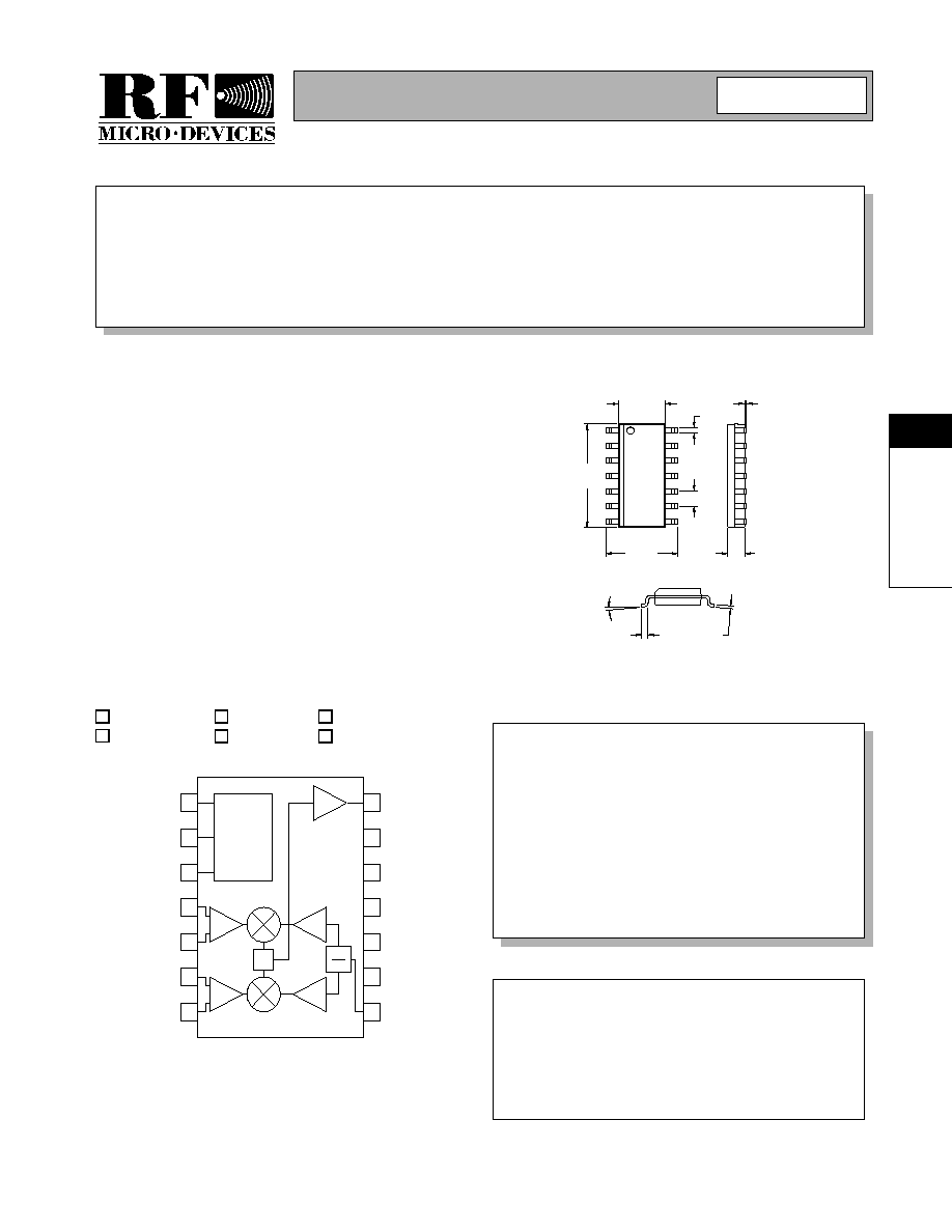
0.156
0.148
0.059
0.057
0.252
0.236
0.010
0.004
.018
.014
8∞ MAX
0∞ MIN
0.0500
0.0164
0.010
0.007
0.347
0.339
0.050
Package Style: SOIC-14
Preliminary
5-56
RF2485
Rev A3 010820
5
M
O
D
U
L
A
T
O
RS
AND
UP
C
O
N
V
E
R
T
E
RS
Absolute Maximum Ratings
Parameter
Rating
Unit
Supply Voltage
-0.5 to +7.5
V
DC
Input LO and RF Levels
+10
dBm
Operating Ambient Temperature
-40 to +85
∞C
Storage Temperature
-40 to +150
∞C
Parameter
Specification
Unit
Condition
Min.
Typ.
Max.
LO Input
T = 25∞C, V
DD
=5V
DC
, I&Q inputs= 2V
PP
Frequency Range
200
600
MHz
Power Level
-3
+6
dBm
Input VSWR
1.2:1
With external 50
termination; see applica-
tion schematic, note A.
Modulation Input
Frequency Range
DC
100
MHz
Reference Voltage (V
REF
)
2.0
3.0
V
Modulation (I&Q)
V
REF
±0.7
V
I & Q signals for -0.5dBm output power.
Modulation (I&Q)
V
REF
±1.5
V
I & Q signals for +5dBm output power.
Maximum Modulation (I&Q)
V
REF
±2.5
V
In-phase and quadrature signals.
Input Resistance
3000
DC Offset
50
150
mV
I
SIG
-I
REF
and Q
SIG
-Q
REF
; to achieve maxi-
mum carrier suppression.
Amplitude Error (I/Q)
0.2
dB
Quadrature Phase Error
±1
±3
∞
From 350MHz to 450MHz.
RF Output
V
DD
=5V, LO Power= 0dBm, LO
Freq= 400MHz, SSB, I&Q input= 0.7V
P
Output Power
-1.5
-0.5
dBm
Output Impedance
50
Output VSWR
1.5:1
Broadband Noise Floor
-149
-147
dBm/Hz
At 5MHz offset
Sideband Suppression
30
43
dB
Unadjusted
Carrier Suppression
20
26
dB
Modulation DC offset can be externally
adjusted for optimum suppression. Suppres-
sion is typically better than 25dB without
adjustment.
IM3
-40
-52
dBc
TETRA Modulation
Channel Power
-3.0
-2.5
-2.0
dBm
1.7V
P-P
TETRA Modulation
LO, 450MHz@ -5.0dBm, V
REF
2.5V
Adjacent Channel Power
Rejection
dBc
VCC= 5.0V
25kHz
-47.0
-48.0
-49.0
dBc
50kHz
-67.0
-68.5
-70.0
dBc
Power Supply
Voltage
5
V
Specifications
4.5
5.5
V
Operating Limits
Current
28
39
mA
Operating
Caution! ESD sensitive device.
RF Micro Devices believes the furnished information is correct and accurate
at the time of this printing. However, RF Micro Devices reserves the right to
make changes to its products without notice. RF Micro Devices does not
assume responsibility for the use of the described product(s).
Preliminary
5-57
RF2485
Rev A3 010820
5
M
O
D
U
L
A
T
O
RS
AND
UP
C
O
N
V
E
R
T
E
RS
Pin
Function
Description
Interface Schematic
1
VDD2
Power supply for the RF Output amplifier. An external RF bypass
capacitor is needed. The trace length between the pin and the bypass
capacitor should be minimized. The ground side of the capacitor should
connect immediately to the ground plane.
2
VDD1
Power supply for all other circuits. An external RF bypass capacitor is
needed.
3
NC
No connection.
4
I SIG
Baseband input to the I mixer. This pin is DC coupled. Maximum output
power is obtained when the input signal has a peak to peak amplitude
of 5V. The DC level supplied to this pin should be 2.5± 0.5V. The SIG
and REF inputs are inputs of a differential amplifier. Therefore the REF
and SIG inputs are interchangeable. If swapping the I SIG and I REF
pins, the Q SIG and Q REF also need to be swapped to maintain the
correct phase. It is also possible to drive the SIG and REF inputs in a
balanced mode. This will increase the gain.
5
I REF
Reference voltage for the I mixer. This voltage should be the same as
the DC voltage supplied to the I SIG pin. To obtain a carrier suppres-
sion of better than 40dB it may be tuned ±0.15V (relative to the I SIG
DC voltage). Without tuning, it will typically be better than 25dB.
See pin 4.
6
Q REF
Reference voltage for the Q mixer. This voltage should be the same as
the DC voltage supplied to the Q SIG pin. To obtain a carrier suppres-
sion of better than 40dB it may be tuned ±0.15V (relative to the Q SIG
DC voltage). Without tuning, it will typically be better than 25dB. The
SIG and REF inputs are inputs of a differential amplifier. Therefore the
REF and SIG inputs are interchangeable. If swapping the I SIG and I
REF pins, Q SIG and Q REF also need to be swapped to maintain cor-
rect phase. It is also possible to drive the SIG and REF inputs in a bal-
anced mode. This will increase the gain.
Same as pin 3.
7
Q SIG
Baseband input to the Q mixer. This pin is DC coupled. Maximum out-
put power is obtained when the input signal has a peak to peak ampli-
tude of 5V. The DC level supplied to this pin should be 2.5± 0.5V.
Same as pin 4.
8
LO IN
The input of the phase shifting network. This high impedance input can
be matched with an external 56
termination resistor. This pin is inter-
nally connected to ground through a 4k
resistor. Putting a DC voltage
on this pin is not recommended. However, connecting this pin to
ground, e.g., through a shunt inductor, is allowed.
9
PHASE
This pin allows to adjust the phase of the I/Q signals. However, the con-
trol is very sensitive and hard to control. Control voltage change for a
few degrees adjustment is in the order of 10mV. Device to device and
temperature variation are not characterized. Therefore it is not recom-
mended to use this pin; leave it not connected. Do NOT connect to
ground.For compensating large errors in the I/Q signals supplied to the
device or in control loops this pin may prove useful.
10
GND1
Ground connection of the LO phase shift network. This pin should be
connected directly to the ground plane.
11
GND
Ground connection for other circuits. Keep traces short and connect to
ground plane immediately.
12
GND
Same as pin 11.
13
GND2
Ground connection for the RF output stage. A good ground connection
is especially important at this pin to avoid interference with other cir-
cuits.
I SIG
I REF
LO IN
PHASE

Preliminary
5-58
RF2485
Rev A3 010820
5
M
O
D
U
L
A
T
O
RS
AND
UP
C
O
N
V
E
R
T
E
RS
Pin
Function
Description
Interface Schematic
14
RF OUT
50
output. This pin carries a DC voltage, and an external blocking
capacitor is recommended.
RF OUT
Preliminary
5-59
RF2485
Rev A3 010820
5
M
O
D
U
L
A
T
O
RS
AND
UP
C
O
N
V
E
R
T
E
RS
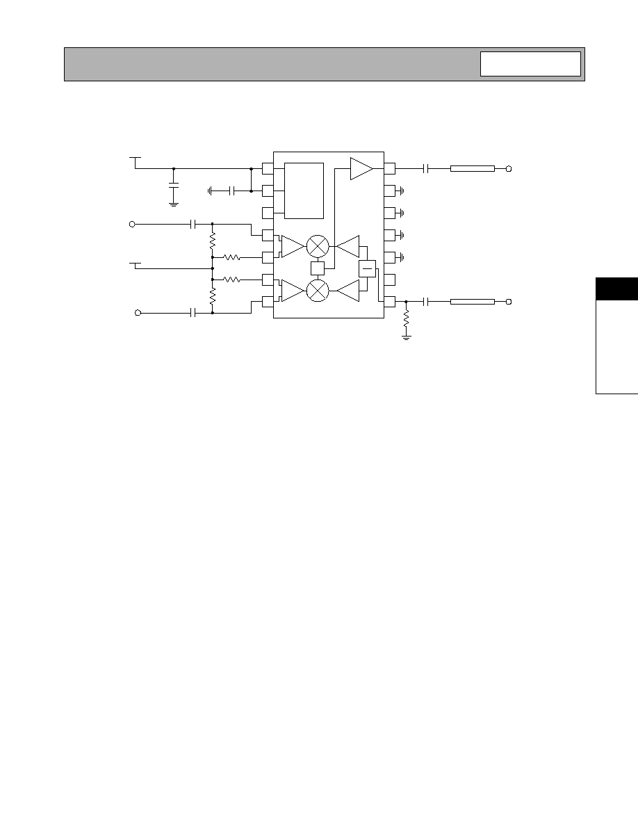
Application Schematic
POWER
CONTROL
+45∞
-45∞
RF OUTPUT
LO INPUT
V
DD
I INPUT
Z
IN
=100
V
REF
Q INPUT
Z
IN
=100
50
µ
strip
Coupling Capacitor
Coupling Capacitor
100
100
100
100
100 pF
100 nF
56
Note A
100 pF
100 pF
50
µ
strip
Optional; input impedance is about 79-J158
at 400 MHz
without resistor. SMD resistor mounted adjacent to package pin,
grounded through a via to the ground plane.
NOTE A:
1
2
3
4
5
6
7
14
13
12
11
10
9
8
NC