
7-39
7
Q
U
ADR
A
T
U
RE
DEM
O
DU
L
A
T
O
R
S
Preliminary
Product Description
Ordering Information
Typical Applications
Features
Functional Block Diagram
RF Micro Devices, Inc.
7628 Thorndike Road
Greensboro, NC 27409, USA
Tel (336) 664 1233
Fax (336) 664 0454
http://www.rfmd.com
Optimum Technology Matching� Applied
Si BJT
GaAs MESFET
GaAs HBT
Si Bi-CMOS
�
SiGe HBT
Si CMOS
7
GN
D
Gain
Control
Div
4
I/Q
Cal
Mode Control
& Biasing
8
LO
4
W-CDMA IN+
2
NC
6
VC
C
20
VG
C
2
1
VG
C
1
17
IF
+
14 I OUT+
15 ENCAL
16 FCLK
11 Q OUT-
19 VREF2V
10
EN
R
X
3
NC
5
W-CDMA IN-
9
EN
WU
P
12 Q OUT+
13 I OUT-
18
IF
-
RF2690
W-CDMA RECEIVE AGC
AND DEMODULATOR
� W-CDMA Systems
The RF2690 is an integrated complete IF AGC amplifier
and quadrature demodulator designed for the receive
section of W-CDMA applications. It is designed to amplify
received IF signals, while providing 70 dB of gain control
range, a total of 90dB gain, and demodulation to base-
band I and Q signals. This circuit is designed as part of
RFMD's single mode W-CDMA chipset, which includes
the RF9678 as modulator and IF AGC and the RF2638 as
upconvertor. The IC is manufactured on an advanced
25GHz F
T
Silicon Bi-CMOS process, and is packaged in
a 20-pin, 4mmx4mm, leadless chip carrier.
� Digitally Controlled Power Down Mode
� 2.7V to 3.3V Operation
� Digital LO Quadrature Divide-by-4
� IF AGC Amp with 70dB Gain Control
� 80dB Maximum Voltage Gain
RF2690
W-CDMA Receive AGC and Demodulator
RF2690 PCBA
Fully Assembled Evaluation Board
7
Rev A4 010918
1.00
0.90
4.00
sq.
0.60
0.24 typ
3
0.20
0.75
0.50
0.23
0.13
4 PLCS
0.50
2.10
sq.
0.65
0.30
4 PLCS
0.05
12�
MAX
Dimensions in mm.
Note orientation of package.
NOTES:
Package Warpage: 0.05 mm max.
4
Die Thickness Allowable: 0.305 mm max.
5
Pin 1 identifier must exist on top surface of package by identification
mark or feature on the package body. Exact shape and size is optional.
2
Shaded lead is Pin 1.
1
Dimension applies to plated terminal: to be measured between 0.02 mm
and 0.25 mm from terminal end.
3
Package Style: LCC, 20-Pin, 4x4
Preliminary
7-40
RF2690
Rev A4 010918
7
Q
U
ADR
A
T
U
RE
DEM
O
DU
L
A
T
O
R
S
Absolute Maximum Ratings
Parameter
Rating
Unit
Supply Voltage
-0.5 to +5
V
DC
Power Down Voltage (V
PD
)
-0.5 to V
CC
+0.7
V
DC
Input RF Power
+3
dBm
Ambient Operating Temperature
-40 to +85
�C
Storage Temperature
-40 to +150
�C
Parameter
Specification
Unit
Condition
Min.
Typ.
Max.
Overall Inputs and AGC
Temp= 25�C, V
CC
=3V, Z
LOAD
=60k
diff.,
LO= 760MHz@-10dBm, Z
SOURCE
=500
diff.
IF Frequency
190
MHz
W-CDMA IF Input Impedance
1200
Single-ended
2400
Balance. An external resistor across the dif-
ferential input is used to define the input
impedance.
LO Frequency
760
MHz
LO Input Level
-20
-10
0
dBm
LO Input Impedance
50
Single-ended.
Maximum Voltage Gain
76
81
dB
Pin-to-Pin voltage gain.
Note: 10dB additional voltage gain in input
match 50
to 500
.
Minimum Voltage Gain
5
12
15
Gain Variation versus V
CC
and
Temperature
-3
+1
+3
dB
Gain Control Voltage
0.3
2.4
V
Defined with external 10k
resistor in series
with V
GC1
pin. Analog gain control.
Input IP3
Blockers at 10MHz and 20MHz offset.
-52
-48
dBm
Maximum Gain. V
GC
= 2.4V
-5
0
dBm
Minimum Gain. V
GC
= 0.3V
Noise Figure
5
dB
Maximum Gain. V
GC
= 2.4V
Inband Output 1dB Compression
1.5
2.0
V
P-P
Measured differentially.
Compression
Out of band blocker causing 1dB of inband
gain compression. Blocker at 5MHz.
-48
dBm
Maximum Gain. V
GC
= 2.4V
-17
dBm
Minimum Gain. V
GC
= 0.3V
Butterworth third order, F
C
2.5M +10%
Baseband 3dB Bandwidth
2.25
2.5
2.75
MHz
Calibrated. F
CLK
=13MHz
Sideband Suppression
27
dB
A measure of IQ gain match and IQ quadra-
ture accuracy. Measured for baseband fre-
quencies 100kHz to 2.5MHz.
DC Offset
+40
mV
Baseband External Load
20
60
k
Resistive Load Impedance.
Differentially across pins.
5
pF
Capacitive Load Impedance.
To ground.
Output DC Voltage
V
CC
- 1.3
V
CC
-1.6
V
CC
- 1.9
V
IQ Amplitude Balance
+0.2
+0.5
dB
V
GC
= 0.3V, P
IN
= -40dBm
IQ Phase Balance
+2
+5
degree
V
GC
= 0.3V, P
IN
= -40dBm
Caution! ESD sensitive device.
RF Micro Devices believes the furnished information is correct and accurate
at the time of this printing. However, RF Micro Devices reserves the right to
make changes to its products without notice. RF Micro Devices does not
assume responsibility for the use of the described product(s).

Preliminary
7-41
RF2690
Rev A4 010918
7
Q
U
ADR
A
T
U
RE
DEM
O
DU
L
A
T
O
R
S
1
Bondout option available for 15.36MHz, 18MHz and 19 MHz.
Parameter
Specification
Unit
Condition
Min.
Typ.
Max.
Auto Calibration
F
CLK
Input Frequency
1
13
MHz
F
CLK
Signal Level
0.4
1.0
V
P-P
F
CLK
Pin Input Impedance
20
k
Single-ended.
Calibration Time
200
us
Current, Auto Cal.
1
mA
Disabled after calibration.
Current, Once Auto Cal Finished
1
uA
CALEN
TBD
DC Specifications
Supply Voltage
2.7
3.0
3.3
V
Current Consumption
Power Down
<1
�
A
W-CDMA Warm-up
5
mA
W-CDMA
8
mA
Logic Levels
V
EN
High Voltage
1.8
V
CC
V
V
EN
Low Voltage
0
0.5
V

Preliminary
7-42
RF2690
Rev A4 010918
7
Q
U
ADR
A
T
U
RE
DEM
O
DU
L
A
T
O
R
S
Auto Calibration Mode
The filters are automatically tuned when the ENCAL pin goes high. The filters are reset to a nominal value whenever the
ENCAL pin goes low. The auto calibration circuitry is independent of the EN WUP and the EN RX control pins.
The EN RX and ENCAL pins can be connected together if desired.
Mode Control Truth Table
Logic
Mode
EN RX
EN WUP
Power Down
0
X
W-CDMA RX Warm-Up
1
0
W-CDMA RX
1
1
EN RX
Chip Enable
If EN RX= 0, then entire IC is powered down.
EN WUP
Warm-up Enable
If EN WUP= 0, then IC is in warm-up mode.
Preliminary
7-43
RF2690
Rev A4 010918
7
Q
U
ADR
A
T
U
RE
DEM
O
DU
L
A
T
O
R
S
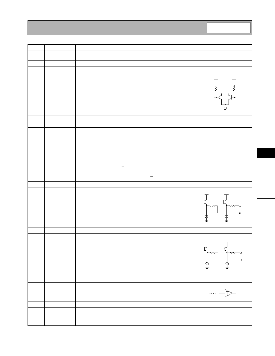
Pin
Function
Description
Interface Schematic
1
VGC1
Analog gain control. Valid control voltage ranges are from 0.5V to 2.5V.
These voltages are valid with a 10k
resistor in series with GC pin.
2
NC
Unused. Connect to signal ground in application.
3
NC
Unused. Connect to signal ground in application.
4
W-CDMA
IN+
W-CDMA balanced input pin. This pin is internally DC-biased and
should be DC-blocked if connected to a device with a DC level present.
For single-ended input operation, one pin is used as an input and the
other W-CDMA input is AC coupled to ground. The balanced input
impedance is 2.4k
, while the single-ended input impedance is 1.2k
.
5
W-CDMA
IN-
Same as pin 4, except complementary input.
See pin 4.
6
VCC
Supply
7
GND
Connect to ground.
8
LO
LO input pin. This input is internally DC-biased and should be DC-
blocked if connected to a device with DC present. The frequency of the
signal applied to this pin is internally divided by a factor of four, hence
the LO applied should be four times the frequency of the IF.
9
EN WUP
Warm-up mode enable. The input LO buffers and divider chains are
enabled. When logic "low" (<0.5V), chip is in warm-up mode. When
logic "high" (VCC -0.3V), chip is in W-CDMA RX mode.
10
EN RX
Chip enable. Power down. When logic "low" (< 0.5V), all circuits are
turned off. When logic "high" (VCC -0.3V), all circuits are operating.
11
Q OUT-
Complementary output to Q OUT+.
12
Q OUT+
Balanced baseband output of Q mixer. This pin is internally DC-biased
and should be DC-blocked externally. The output may be used single-
ended by leaving one of the pins unconnected, however half of the out-
put voltage will be lost.
13
I OUT-
Complementary output to I OUT+.
14
I OUT+
Balanced baseband output.
15
ENCAL
Calibration enable.
16
FCLK
F
CLK
clock reference for the automatic calibration circuitry.
17
IF-
Complementary output to IF+.
18
IF+
IF test point output. This balanced node is pinned out to allow for moni-
toring of the AGC output signal as it enters the demodulator. During
normal operation, this pin and its complementary output should be left
floating and not connected.
1200
1200
W-CDMA IN+
BIAS
BIAS
W-CDMA IN-
150
�
A
Q OUT-
Q OUT+
V
CC
V
CC
150
�
A
150
�
A
I OUT-
I OUT+
150
�
A
V
CC
V
CC
20 k

Preliminary
7-44
RF2690
Rev A4 010918
7
Q
U
ADR
A
T
U
RE
DEM
O
DU
L
A
T
O
R
S
Pin
Function
Description
Interface Schematic
19
VREF2V
2V voltage reference decouple (i.e., 10nF to ground).
20
VGC2
Gain control decouple (i.e., 10nF to ground).
Pkg
Base
Die
Flag
Ground.

Preliminary
7-45
RF2690
Rev A4 010918
7
Q
U
ADR
A
T
U
RE
DEM
O
DU
L
A
T
O
R
S
Application Notes
Voltage Gain Measurement Set-up
The evaluation board uses a unity voltage gain Op-Amp to simulate the 60k
differential load impedance condition for
the chip. The 50
output impedance of Op-Amp makes the use of a 50
spectrum analyzer power measurement possi-
ble. The power gain measured will be considered as RAW Gain. The input impedance of the chip is 500
differential by
adding a parallel 680
resistor. The input transformer matches 50
to 500
and results in 10 dB difference between
voltage gain and power gain, hence, the voltage gain of the chip is RAW Gain minus 10dB. Because the input trans-
former loss is 0.8 dB, it needs to be added to the gain. Since the Op-Amp has the unity voltage gain, the voltage at the
evaluation board output is the same as the voltage at chip I or Q output. Therefore, the voltage gain of the chip with 60 k
load can be calculated by
Gv= RAW Gain -10+ 0.8 (dB)
Input IP3 Measurement
The input IP3 measurement is based on a two tone inter-modulation test condition from the 3GPP standard, which spec-
ifies two tones with offset frequencies at 10MHz and 20 MHz. Due to the on-chip baseband filtering, the two tone output
is attenuated and cannot be seen. Since the only parameter observable is the IM3 product, the input IP3 then is calcu-
lated by
IIP3 =Pin+ 0.5*(Pin+ RAW Gain-IM3)
Noise Figure Measurement
The noise figure measurement is based on the noise figure definition NF= N
O
-N
I
-Gain, where N
O
is the output noise
density, N
I
is the input noise density (-174 dBm/Hz when no input signal is applied) and Gain is the RAW Gain. The out-
put noise density N
O
is measured at 1MHz offset when no signal input is applied. The NF is calculated by NF= N
O
-
174 dBm/Hz-RAW Gain. Since the I and Q re-combination will provide 3dB extra for signal-to-noise ratio, the actual
noise figure is should be reduced by 3dB. In addition, noise figure should be reduced by the input transformer loss of
0.8dB. Therefore, the NF is calculated by
NF =N
O
+ 174-RAW Gain-3-0.8(dB)
1 dB Gain Compression Point Voltage at Baseband Output
The device has a relatively constant 1 dB gain compression point versus V
GC
. Gain compression is tested with a CW sig-
nal with 60 k
load differential.
How to Calculate the Power Gain of the Demodulator
In the system analysis for cascaded gain, noise and IP, it is often required to calculate the power gain of the demodulator
chip itself in matched load condition. Below is an example on how to determine this power gain value.
For this example, the load impedance is 60k
differential, the output AC impedance of the I or Q port is 500
, the mea-
sured RAW Gain is 95 dB.
First, the power gain from the input of the chip to the input of Op-Amp needs to be calculated. Since the voltage at the
50
load and the voltage at Op-Amp input are the same, the difference of the power gain across the Op-Amp is the ratio
of load impedances. Hence, the power gain to the Op-Amp input is 95dB-10 log(60000/50)=95-30=65dB.
Second, the power gain of the demodulator itself with matched load is calculated. The mismatch coefficient a is deter-
mined by the mismatch coefficient equation
10
4R
S
R
L
R
S
R
L
+
(
)
2
--------------------------
log
10
4 500 60000
500
60000
+
(
)
2
-------------------------------------
log
15dB
�
=
=
=

Preliminary
7-46
RF2690
Rev A4 010918
7
Q
U
ADR
A
T
U
RE
DEM
O
DU
L
A
T
O
R
S
Since the power gain to the input of the Op-Amp G
P
'=
G
P
, where G
P
is the power gain of demodulator for matched load.
Therefore, the demodulator power gain is 65+ 15 =80dB.
AC Coupling in Evaluation Board
The output I and Q baseband signal is AC coupled for evaluation purposes only. The high-pass corner frequency is at
1/(2
RC)=1/ (6.28* 30k
*100 nF)=56Hz.
I and Q Output DC Voltage and Its Offset
Although the I and Q output is AC coupled on the evaluation board, in most applications, it would be DC coupled to the
ADC input buffer. The DC voltage at the IC output is V
CC
-1.6V with a possible variation of �0.3 V due to temperature and
tolerance. The differential circuit asymmetry would cause common mode DC offset to the extent of �40mV.
Baseband Filter Calibration Process
The BB (baseband) filter calibration process is same for both WCDMA and GSM/DCS. After calibration is done, the
WCDMA mode sets the circuitry to have a 3 dB bandwidth of 2.5MHz, the GSM/DCS mode (if the chip has GSM/DCS
mode) sets the circuitry to have a 3dB bandwidth of 250kHz.
The BB filter in the I and Q path needs to be calculated every time after power down. When the FCLK pin is connected to
a signal generator with 0dBm output level at 13.0MHz, a logic high at CALEN pin for 200
�
s will calibrate the filter to have
2.5 MHz bandwidth with 10% accuracy when WCDMA mode is set, or to 250kHz bandwidth with 10% accuracy when
GSM mode is set. The calibration is done when the chip is powered on only. Calibration is independent from all other
conditions, e.g. the chip enable could be off.
The calibration circuitry consumes 400
�
A. When the calibration sequence is complete after 200
�
s, the I
CC
drops to
0mA.
The 3dB bandwidth is defined to be from the reference level at 1 MHz for WCDMA and at 50 kHz for GSM/DCS. The 3 dB
bandwidth is independent of V
GC
and V
CC
.
The filter can also be calibrated with different clock frequencies from 10MHz to 30MHz to tune the bandwidth over -40%
to +60% from its default 3dB bandwidth (2.5MHz for WCDMA and 250kHz for GSM). The 3dB bandwidth is linear with
clock frequency.
Preliminary
7-47
RF2690
Rev A4 010918
7
Q
U
ADR
A
T
U
RE
DEM
O
DU
L
A
T
O
R
S
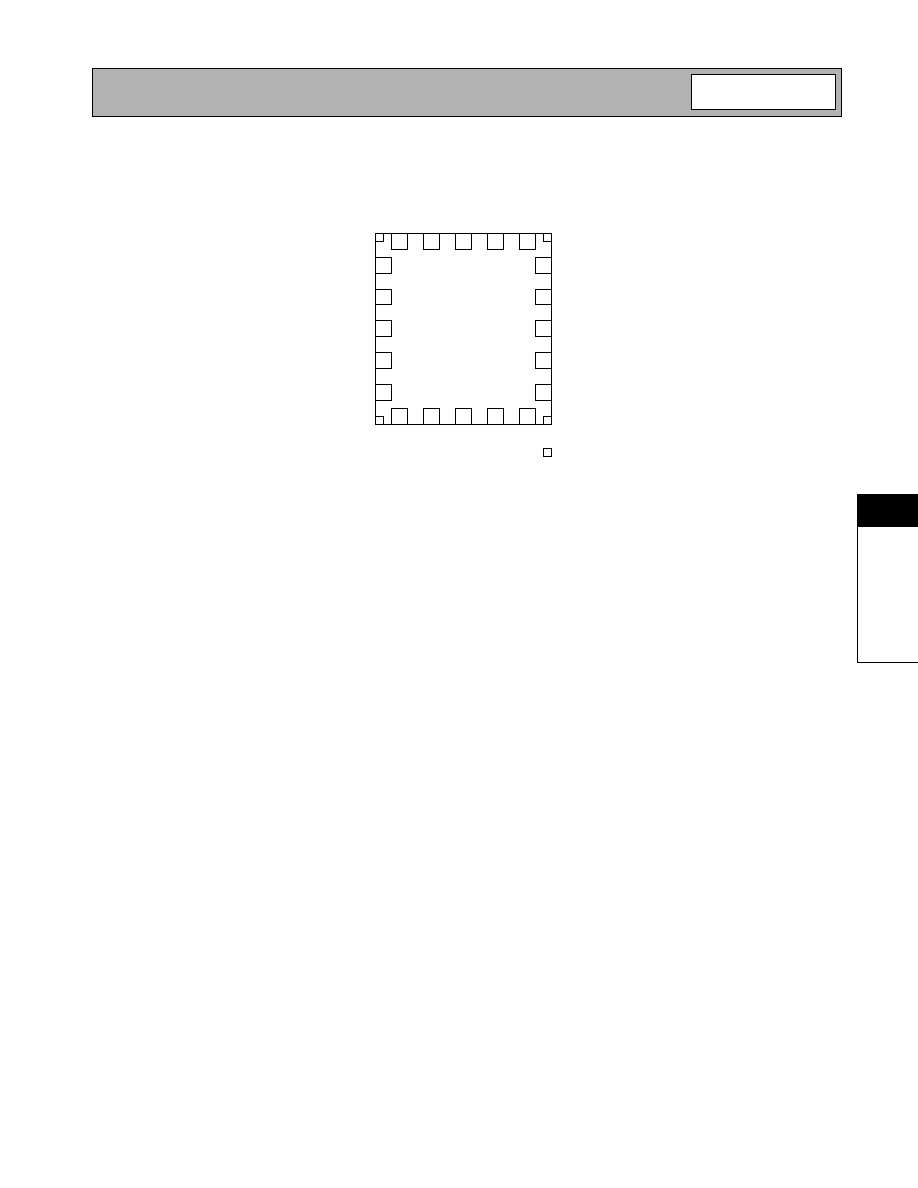
Pin Out
19
VR
EF
2
V
18
17
IF
-
16
FC
LK
14
13
12
10
EN
R
X
9
8
LO
7
GN
D
5
4
3
2
NC
1
VGC1
*
*
*
*
20
VG
C
2
VC
C
6
11 Q OUT-
15 ENCAL
*
Represents "GND".
NC
W-CDMA IN+
W-CDMA IN-
EN
W
U
P
Q OUT+
I OUT-
I OUT+
IF
+

Preliminary
7-48
RF2690
Rev A4 010918
7
Q
U
ADR
A
T
U
RE
DEM
O
DU
L
A
T
O
R
S
Application Schematic
1
3
6
4
5
2
7
8
9
10
19
20
16
13
15
14
10 nF
10 k
10 nF
VGC
100 nF
V
CC
I OUT N
EN RX
10 nF
1 nF
I OUT P
18
17
12
11
10 nF
VREF 2V
10 pF
FCLK
ENCAL
100 nF
100 nF
Q OUT N
Q OUT P
100 nF
EN WUP
LO IN
2.4 k
Balanced
10 nF
W-CDMA

Preliminary
7-49
RF2690
Rev A4 010918
7
Q
U
ADR
A
T
U
RE
DEM
O
DU
L
A
T
O
R
S
Evaluation Board Schematic
(Download Bill of Materials from www.rfmd.com.)
Drawing 2690400 Rev -
19
18
17
16
14
13
12
10
9
8
7
5
4
3
2
1
*
*
*
*
20
6
11
15
R1
10 k
VGC
C2
5.1 pF
C4*
DNI
50
�
strip
J2
WCDMA
C6
100 pF
R7
680
L2
150 nH
C10
10 nF
VCC
ENWUP
C23*
DNI
C20
100 pF
C24*
DNI
50
�
strip
J4
LO IN
ENRX
TP7
Q OUT N
TP6
Q OUT P
TP5
I OUT N
TP4
I OUT P
R12*
DNI
C12
100 nF
R2
10 k
C13
100 nF
R3
10 k
R14
20 k
3
2
+
-
C14
100 nF
+5V
7
4
8
5
U2
R15
20 k
6
CLC426
R18
51
50
�
strip
J5
IOUT
C15
100 nF
-5V
R13*
DNI
C18
100 nF
R4
10 k
C19
100 nF
R5
10 k
R16
20 k
3
2
+
-
C16
100 nF
+5V
7
4
8
5
U3
R17
20 k
6
CLC426
R19
51
50
�
strip
J6
QOUT
C17
100 nF
-5V
ENCAL
C9
100 pF
C8
1 nF
TP1
VREF2V
TP2
IFP
TP3
IFN
C11
10 pF
J3
FCLK
CON3
JP3
+5V
-5V
1
2
3
C21
1 uF(16V) +
C22
1 uF(16V)
+
HDR 8
8
7
6
5
4
3
2
1
JP1
ENRX
ENCAL
ENWUP
VCC
VGC
C7
1 uF
+
R10
1 M
R9
1 M
R8
1 M

Preliminary
7-50
RF2690
Rev A4 010918
7
Q
U
ADR
A
T
U
RE
DEM
O
DU
L
A
T
O
R
S
Evaluation Board Layout
Board Size 3.1" x 3.0"
Board Thickness 0.032", Board Material FR-4

Preliminary
7-51
RF2690
Rev A4 010918
7
Q
U
ADR
A
T
U
RE
DEM
O
DU
L
A
T
O
R
S
Preliminary
7-52
RF2690
Rev A4 010918
7
Q
U
ADR
A
T
U
RE
DEM
O
DU
L
A
T
O
R
S
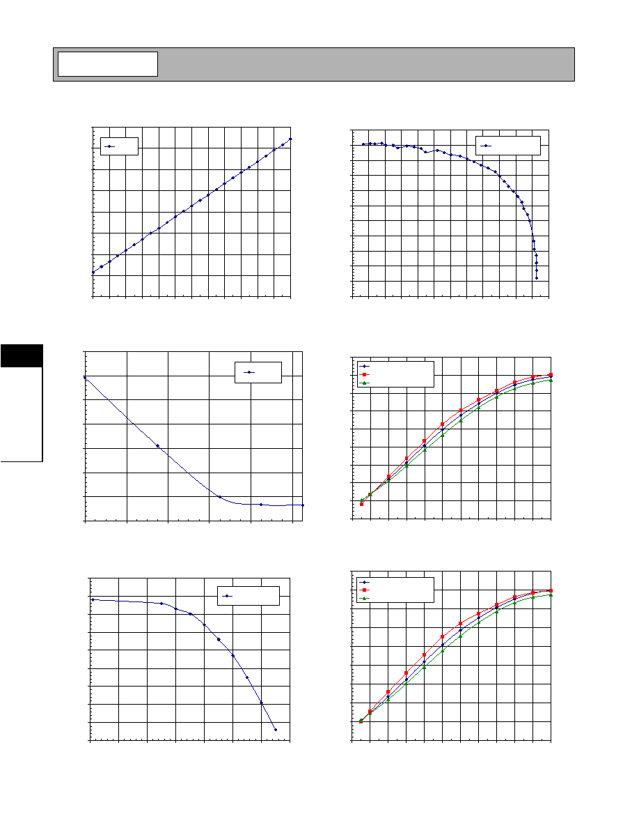
NF versus V
GC
IF Freq. 190MHz, LO Freq. 760MHz @ -10dBm, V
CC
=3.0, V
GC
=2.4 to 0.3V)
0.0
10.0
20.0
30.0
40.0
50.0
60.0
70.0
0.3
0.7
1.1
1.5
1.9
2.3
Vgc (V)
NF
(dB)
NF[dB]
Voltage Gain versus V
GC
(Temp. +25
o
C, - 40
o
C, +85
o
C)
(IF Freq. 190MHz, LO Freq. 760MHz @ -10dBm,V
CC
=2.7V,V
GC
=2.4V to 0.3V)
0.0
10.0
20.0
30.0
40.0
50.0
60.0
70.0
80.0
90.0
0.2
0.4
0.6
0.8
1.0
1.2
1.4
1.6
1.8
2.0
2.2
2.4
V
GC
(V)
Voltage
Gain
(dB)
Gain @2.7V,Temp.+25C
Gain @2.7V,Temp.- 40C
Gain @2.7V,Temp.+85C
Voltage Gain versus P
OUT
(1dB Compression)
(V
CC
=3.0V, V
GC
=2.4V, IF=191MHz, LO=760MHz @ -10dBm)
70.0
71.0
72.0
73.0
74.0
75.0
76.0
77.0
78.0
79.0
80.0
81.0
500
600
700
800
900 1000 1100 1200 1300 1400 1500 1600 1700
Power Out (mV-peak)
Voltage
Gain
(dB)
Voltage Gain [dB]
W-CDMA Baseband Filter Response (Calibrated)
(IF=190MHz to 195MHz, LO=760MHz @ -10dBm, V
CC
=3.0V, V
GC
=2.4V)
-1.0
0.0
1.0
2.0
3.0
4.0
5.0
6.0
7.0
8.0
0.0
0.5
1.0
1.5
2.0
2.5
3.0
3.5
Frequency (MHz)
Amplitude
(dBm)
Power Out [dBm]
I
GC
versus V
GC
(IF Freq. 190MHz LO Freq. 760MHz V
CC
=3.0V Temp. 25
o
C)
-25.0
-20.0
-15.0
-10.0
-5.0
0.0
5.0
10.0
15.0
0.0
0.2
0.4
0.6
0.8
1.0
1.2
1.4
1.6
1.8
2.0
2.2
2.4
V
GC
(V)
I
GC
(uA)
Igc [uA]
Voltage Gain versus V
GC
(Temp. +25
o
C, - 40
o
C, +85
o
C)
(IF Freq. 190MHz, LO Freq. 760MHz @ -10dBm, V
CC
=3.0V, V
GC
=2.4V to 0.3V)
0.0
10.0
20.0
30.0
40.0
50.0
60.0
70.0
80.0
90.0
0.2
0.4
0.6
0.8
1.0
1.2
1.4
1.6
1.8
2.0
2.2
2.4
V
GC
(V)
Voltage
Gain
(dB)
Gain @3.0V,Temp.+25C
Gain @3.0V,Temp.- 40C
Gain @3.0V,Temp.+85C
Preliminary
7-53
RF2690
Rev A4 010918
7
Q
U
ADR
A
T
U
RE
DEM
O
DU
L
A
T
O
R
S
Voltage Gain versus V
GC
(Temp. -40
o
C)
(IF Freq. 190MHz, LO Freq. 760MHz @ -10dBm, V
CC
=3.3V, 3.0V, 2.7V, V
GC
=2.4V to 0.3V)
0.0
10.0
20.0
30.0
40.0
50.0
60.0
70.0
80.0
90.0
0.2
0.4
0.6
0.8
1.0
1.2
1.4
1.6
1.8
2.0
2.2
2.4
V
GC
(V
GC
)
Voltage
Gain
(dB)
Gain @3.3V,Temp.- 40C
Gain @3.0V,Temp.- 40C
Gain @2.7V,Temp.- 40C
Voltage Gain versus V
GC
(Temp.+25C, - 40C, +85
o
C)
IF Freq. 190MHz, LO Freq. 760MHz @ -10dBm, V
CC
=3.3V, V
GC
=2.4V to 0.3v)
0.0
10.0
20.0
30.0
40.0
50.0
60.0
70.0
80.0
90.0
0.2
0.4
0.6
0.8
1.0
1.2
1.4
1.6
1.8
2.0
2.2
2.4
V
GC
(V)
Voltage
G
ain
(
dB)
Gain @3.3V,Temp.25C
Gain @3.3V,Temp.- 40C
Gain @3.3V,Temp.+85C
Voltage Gain versus V
GC
(Temp. 25
o
C)
(IF Freq. 190MHz, LO Freq. 760MHz @ -10dBm, V
CC
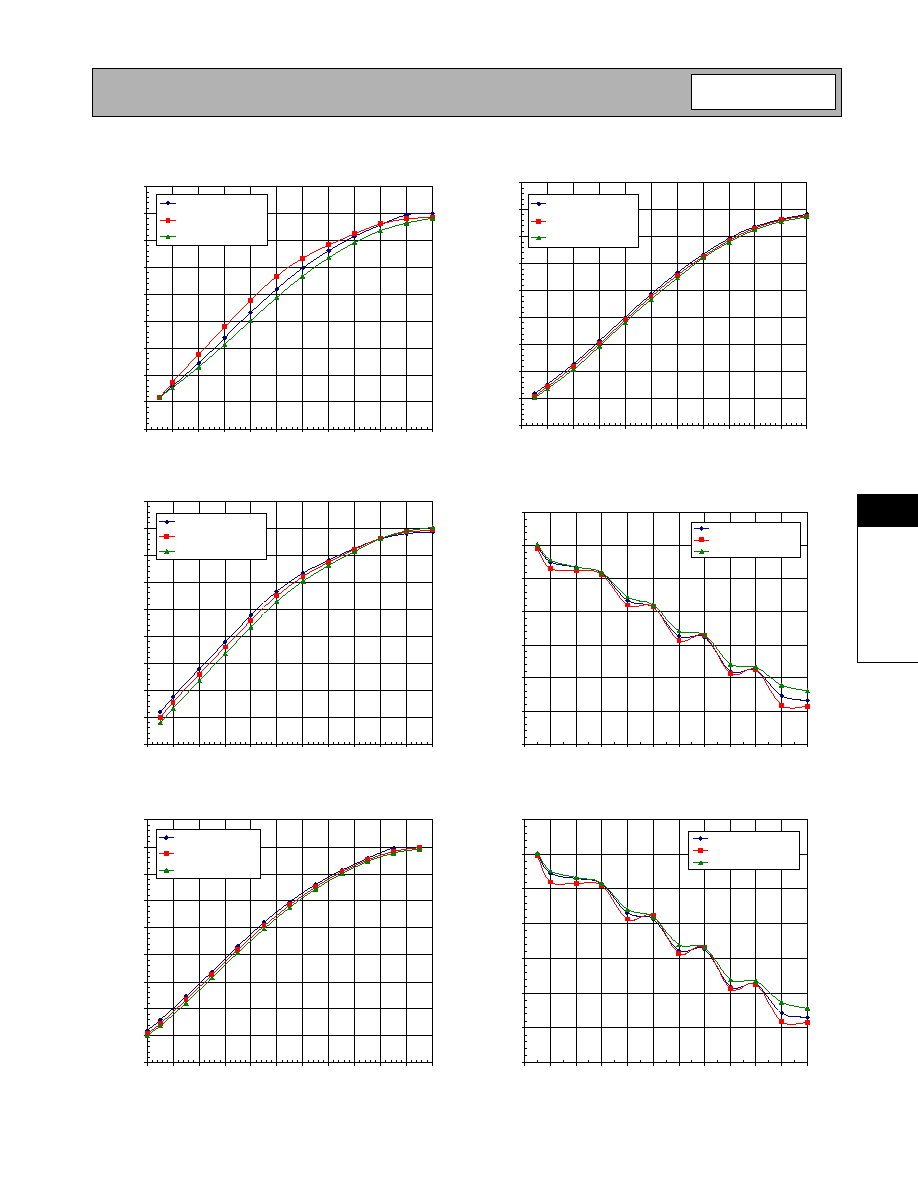
=3.3V, 3.0V, 2.7V & V
GC
=2.4V to 0.3V)
0.0
10.0
20.0
30.0
40.0
50.0
60.0
70.0
80.0
90.0
0.3
0.5
0.7
0.9
1.1
1.3
1.5
1.7
1.9
2.1
2.3
2.5
V
GC
(V)
Voltage
Gain
(dB)
Gain @3.3V,Temp.25C
Gain @3.0V,Temp.25C
Gain @2.7V,Temp.25C
Voltage Gain versus V
GC
(Temp. +85
o
C)
(IF Freq. 190MHz, LO Freq. 760MHz @ -10dBm, V
CC
=3.3V, 3.0V, 2.7V, V
GC
=2.4V to 0.3V)
0.0
10.0
20.0
30.0
40.0
50.0
60.0
70.0
80.0
90.0
0.2
0.4
0.6
0.8
1.0
1.2
1.4
1.6
1.8
2.0
2.2
2.4
V
GC
(V)
Voltage
Gain
(dB)
Gain @3.3V,Temp.+85C
Gain @3.0V,Temp.+85C
Gain @2.7V,Temp.+85C
IIP3 versus V
GC
(Temp. +25
o
C, - 40
o
C, +85
o
C)
(IF Freq.190MHz, LO Freq. 760MHz @ -10dBm, V
CC
=2.7V, V
GC
=2.4V to 0.3V)
-60.0
-50.0
-40.0
-30.0
-20.0
-10.0
0.0
10.0
0.2
0.4
0.6
0.8
1.0
1.2
1.4
1.6
1.8
2.0
2.2
2.4
V
GC
(V)
IIP3
(
dBm)
IIP3 @2.7V,Temp.+25C
IIP3 @2.7V,Temp.- 40C
IIP3 @2.7V,Temp. +85C
IIP3 versus V
GC
(Temp. +25
o
C, - 40
o
C, +85
o
C)
IF Freq. 190MHz, LO Freq. 760MHz @ -10dBm, V
CC
=3.0V, V
GC
=2.4V to 0.3V)
-60.0
-50.0
-40.0
-30.0
-20.0
-10.0
0.0
10.0
0.2
0.4
0.6
0.8
1.0
1.2
1.4
1.6
1.8
2.0
2.2
2.4
V
GC
(V
GC
)
IIP3
(
dBm)
IIP3 @3.0V,Temp.25C
IIP3 @3.0V,Temp.- 40C
IIP3 @3.0V,Temp.+85C

Preliminary
7-54
RF2690
Rev A4 010918
7
Q
U
ADR
A
T
U
RE
DEM
O
DU
L
A
T
O
R
S
IIP3 versus V
GC
(Temp. +25
o
C, - 40
o
C, +85
o
C)
(
IF Freq. 190MHz, LO Freq. 760MHz @ -10dBm, V
CC
=3.3V, V
GC
=2.4V to 0.3V)
-60.0
-50.0
-40.0
-30.0
-20.0
-10.0
0.0
10.0
0.2
0.4
0.6
0.8
1.0
1.2
1.4
1.6
1.8
2.0
2.2
2.4
V
GC
(V)
IIP3
(
dBm)
IIP3 @3.3V,Temp.25C
IIP3 @3.3V,Temp.- 40C
IIP3 @3.3V,Temp. +85C
IIP3 versus V
GC
(Temp. 25
o
C)
(IF Freq. 190MHz, LO Freq. 760MHz @ -10dBm, V
CC
=3.3V ,3.0V, 2.7V, V
GC
=2.4V to 0.3V)
-50.0
-45.0
-40.0
-35.0
-30.0
-25.0
-20.0
-15.0
-10.0
-5.0
0.0
0.2
0.4
0.6
0.8
1.0
1.2
1.4
1.6
1.8
2.0
2.2
2.4
V
GC
(V)
IIP3
(
dBm)
IIP3 @3.3V,Temp.25C
IIP3 @3.0V,Temp.25C
IIP3 @2.7V,Temp.25C
IIP3 versus V
GC
(Temp. +85
o
C)
(IF Freq. 190MHz, LO Freq. 760MHz @ -10dBm, V
CC
=3.3V, 3.0V, 2.7V, V
GC
=2.4V to
0.3V)
-50.0
-45.0
-40.0
-35.0
-30.0
-25.0
-20.0
-15.0
-10.0
-5.0
0.0
5.0
0.2
0.4
0.6
0.8
1.0
1.2
1.4
1.6
1.8
2.0
2.2
2.4
V
GC
(V)
IIP3
(
dBm)
IIP3 @3.3V,Temp. +85C
IIP3 @3.0V,Temp.+85C
IIP3 @2.7V,Temp. +85C
IIP3 versus V
GC
(Temp. -40
o
C)
(IF Freq. 190MHz, LO Freq. 760MHz @ -10dBm, V
CC
=3.3V, 3.0V, 2.7V, V
GC
=2.4V to 0.3V)
-60.0
-50.0
-40.0
-30.0
-20.0
-10.0
0.0
0.2
0.4
0.6
0.8
1.0
1.2
1.4
1.6
1.8
2.0
2.2
2.4
V
GC
(V)
IIP3
(
dBm)
IIP3 @3.3V,Temp.- 40C
IIP3 @3.0V,Temp.- 40C
IIP3 @2.7V,Temp.- 40C