5-113
Product Description
Ordering Information
Typical Applications
Features
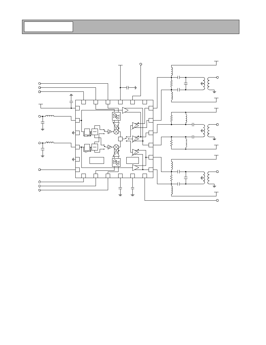
Functional Block Diagram
RF Micro Devices, Inc.
7628 Thorndike Road
Greensboro, NC 27409, USA
Tel (336) 664 1233
Fax (336) 664 0454
http://www.rfmd.com
Optimum Technology MatchingÆ Applied
Si BJT
GaAs MESFET
GaAs HBT
Si Bi-CMOS
SiGe HBT
Si CMOS
InGaP/HBT
GaN HEMT
SiGe Bi-CMOS
VCC2
LO HB P
LO HB N
LO LB P
LO LB N
MODE C
Q SI
G P
MO
D
E
D
Q SI
G N
VREF
GC
D
E
C
GC
RF OUT
LB N
GND
MOD
E
A
VC
C
1
I S
I
G
P
I S
I
G
N
MOD
E
B
7
6
5
4
3
2
1
12
11
10
9
8
18
17
16
15
14
13
23
22
21
20
19
24
Note: The die flag is the
chip's main ground.
+45∞
-45∞
DIV
2
+45∞
-45∞
Flo
x2
Mode Control
and Biasing
Power
Control
RF OUT
LB P
RF OUT
HB N
RF OUT
HB P
RF OUT
WB N
RF OUT
WB P
RF2705
LOW NOISE, MULTI-MODE, QUAD-BAND,
QUADRATURE MODULATOR AND PA DRIVER
∑ EDGE/GSM (GSM850/900) Handsets
∑ EDGE/GSM (DCS/PCS) Handsets
∑ W-CDMA Handsets/Data Cards
∑ W-CDMA/GSM/EDGE Multimode Handsets
and Data Cards
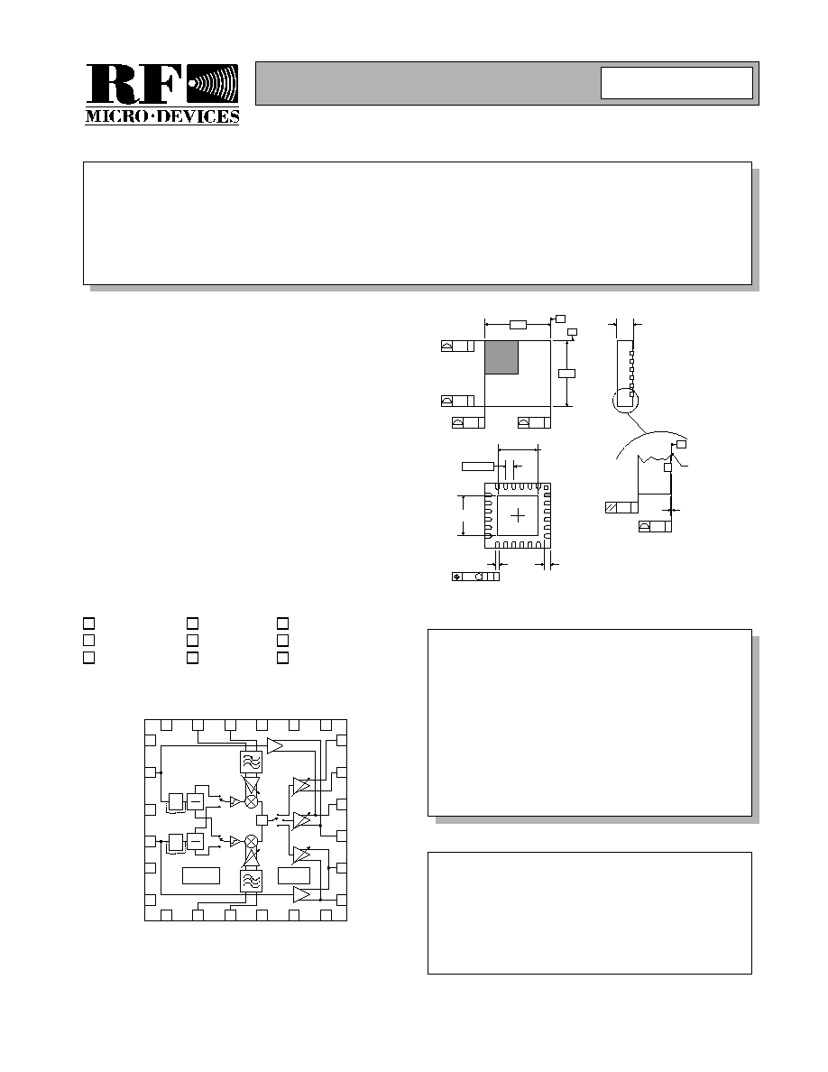
The RF2705 is a low noise, multi-mode, quad-band direct
I/Q to RF modulator and PA driver designed for handset
applications where multiple modes of operation are
required. Frequency doublers, dividers and LO buffers
are included to support a variety of LO generation
options. Dynamic power control is supported through a
single analog input giving 90dB of power control range for
the W-CDMA mode and 40dB of power control in the
other two modes. Three sets of RF outputs are provided:
high band and low band low noise EDGE/GMSK outputs,
as well as one wideband W-CDMA output. The device is
designed for 2.7V to 3.3V operation, and is assembled in
a plastic, 24-pin, 4mmx4mm QFN.
∑ W-CDMA High/Mid/Low Power Modes
∑ Quad-Band Direct Quadrature Modulator
∑ Variable Gain PA Drivers
∑ GMSK Bypass Amplifiers
∑ LO Frequency Doubler and Divider
∑ Baseband Filtering
RF2705
Low Noise, Multi-Mode, Quad-Band, Quadrature
Modulator and PA Driver
RF2705PCBA-41XFully Assembled Evaluation Board
0
Rev A4 041026
4.00
4.00
-B-
-A-
0.10 C
0.10 C
0.10 C
0.10 C
1.00
0.80
SEATING
PLANE
-C-
0.08 C
0.05
0.00
Scale: None
0.10 C
2.45
+0.10
-0.10
2.45
+0.10
-0.10
0.50 TYP
0.10
C A B
M
0.30
0.18
TYP
0.50
0.30
TYP
Dimensions in mm.
Shaded lead is pin 1.
Package Style: QFN, 24-Pin, 4x4

5-114
RF2705
Rev A4 041026
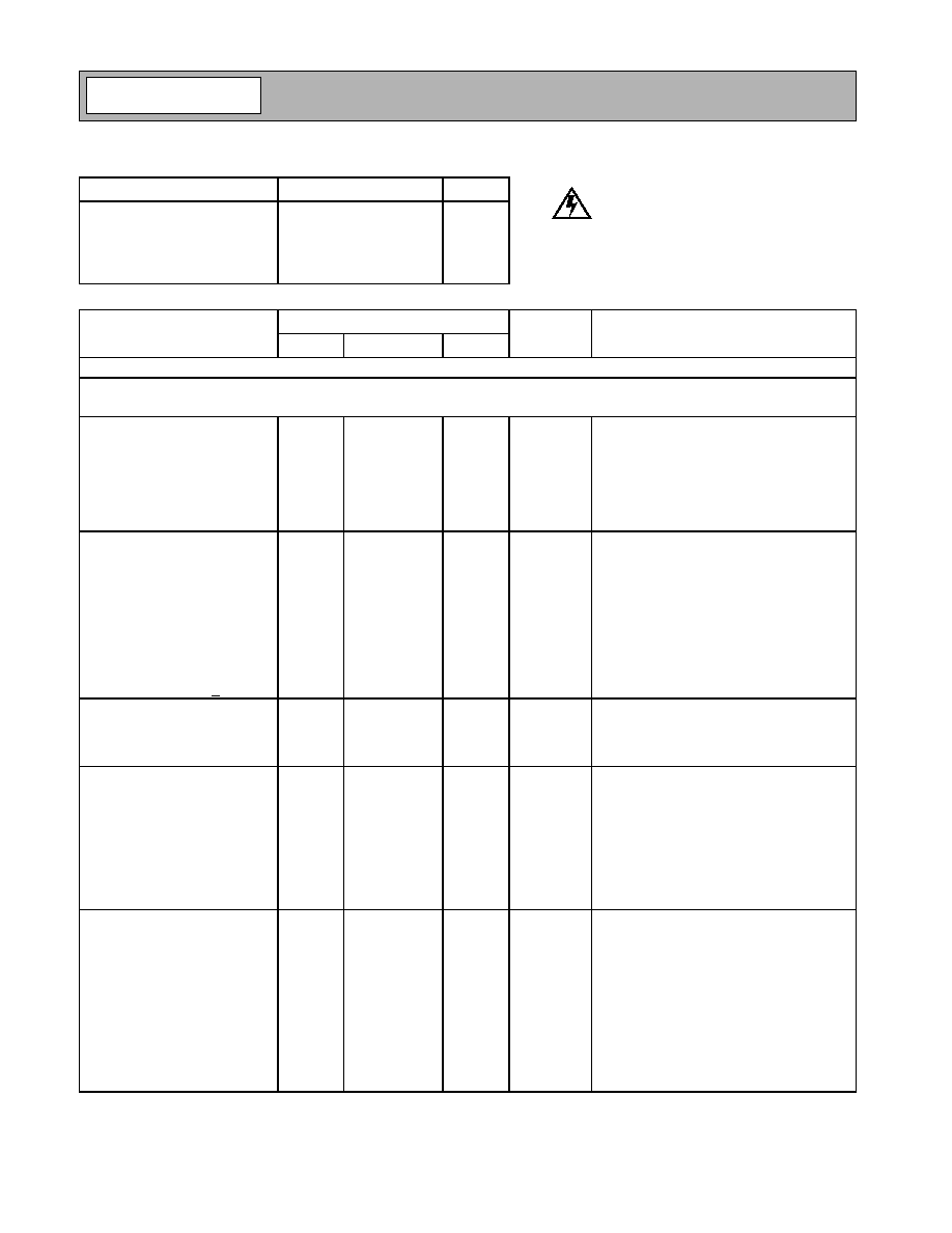
Absolute Maximum Ratings
Parameter
Rating
Unit
Supply Voltage
-0.5 to 3.6
V
Storage Temperature
-40 to +150
∞C
Operating Ambient Temperature
-40 to +85
∞C
Input Voltage, any pin
-0.5 to +3.6
V
Input Power, any pin
+5
dBm
Parameter
Specification
Unit
Condition
Min.
Typ.
Max.
Output Performance with Modulated Baseband Inputs
Low Band EDGE 8PSK Mode (GSM850/GSM900)
Mode=Low Band F
LO
x1 (see Control Logic Truth Table for Mode Control Settings)
Output Power
V
CC
=2.7V, T=+25∞C
Maximum Output Power with
8PSK Modulated Signal*
Maximum VGC
0
+2.5
dBm
While meeting spectral mask
Minimum VGC
-39
-37
dBm
While meeting spectral mask
Gain Range
42
dB
Difference between output power at
GC=2.0V and GC=0.2V.
Out-of-Band Emission
Spectrum Emission Mask*
Frequency Spacing
200kHz
-36
TBD
dBc
30kHz BW
250kHz
-43
TBD
dBc
30kHz BW
400kHz
-67
TBD
dBc
30kHz BW
600kHz to 1800kHz
-73
dBc
30kHz BW
1800kHz to 3000kHz
-73
dBc
100kHz BW
3000kHz to 6000kHz
-73
dBc
100kHz BW
>6000kHz
-75
dBc
100kHz BW
Error Vector Magnitude
8PSK Modulation
RMS*
2
3
%
Origin Offset*
-40
-34
dB
Peak*
4
9
%
Output Noise
At F
C
±20MHz*
Relative Noise at:
Maximum Gain
-156
dBc/Hz
GC=2.0V, IQ=1.2V
P-P
8PSK
-152
dBc/Hz
GC=2.0V to 1.4V
Absolute Noise at:
Maximum Gain
-156
dBm
GC=2.0V, IQ=0V
P-P
All Gain Settings
-154
dBm
IQ=1.2V
P-P
8PSK
General Conditions
Local Oscillator
LO LB Input Frequency
824
915
MHz
RF LB Output Frequency
824
915
MHz
Input Power
-6.0
0.0
+3.0
dBm
IQ Baseband Inputs
8PSK
IQ Level
1.2
V
P-P
Input IQ signal driven differentially and in
quadrature.
IQ Common Mode
1.2
V
Input Bandwidth
0.7
1.0
MHz
Baseband Filter Attenuation
20
dB
At 20MHz offset
* Not tested in Production
Caution! ESD sensitive device.
RF Micro Devices believes the furnished information is correct and accurate
at the time of this printing. However, RF Micro Devices reserves the right to
make changes to its products without notice. RF Micro Devices does not
assume responsibility for the use of the described product(s).

5-115
RF2705
Rev A4 041026
Parameter
Specification
Unit
Condition
Min.
Typ.
Max.
Output Performance with Modulated Baseband Inputs
High Band EDGE 8PSK Mode (DCS1800/PCS1900)
Mode=High Band F
LO
x1 (see Control Logic Truth Table for Mode Control Settings)
Output Power
V
CC
=2.7V, T=+25∞C
Maximum Output Power with
8PSK Modulated Signal*
Maximum VGC
-1
+1.5
dBm
While meeting spectral mask
Minimum VGC
-40
-38
dBm
While meeting spectral mask
Gain Range
42
dB
Difference between output power at
GC=2.0V and GC=0.2V.
Out-of-Band Emission
Spectrum Emission Mask*
Frequency Spacing
200kHz
-36
TBD
dBc
30kHz BW
250kHz
-43
TBD
dBc
30kHz BW
400kHz
-67
TBD
dBc
30kHz BW
600kHz to 1800kHz
-73
dBc
30kHz BW
1800kHz to 3000kHz
-73
dBc
100kHz BW
3000kHz to 6000kHz
-73
dBc
100kHz BW
>6000kHz
-75
dBc
100kHz BW
Error Vector Magnitude
8PSK Modulation
RMS*
1.3
3
%
Origin Offset*
-37
-30
dB
Peak*
3
11
%
Output Noise
At F
C
±20MHz*
Relative Noise at:
Maximum Gain
-154
dBc/Hz
GC=2.0V, IQ=1.2V
P-P
8PSK
-150
dBc/Hz
GC=2.0V to 1.4V
Absolute Noise at:
Maximum Gain
-153
dBm
GC=2.0V, IQ=0V
P-P
All Gain Settings
-151
dBm
IQ=1.2V
P-P
8PSK
General Conditions
Local Oscillator
LO HB Input Frequency
1710
1910
MHz
RF HB Output Frequency
1710
1910
MHz
Input Power
-6.0
0.0
+3.0
dBm
IQ Baseband Inputs
8PSK
IQ Level
1.2
V
P-P
Input IQ signal driven differentially and in
quadrature.
IQ Common Mode
1.2
V
Input Bandwidth
0.7
1.0
MHz
Baseband Filter Attenuation
20
dB
At 20MHz offset
* Not tested in Production

5-116
RF2705
Rev A4 041026
Parameter
Specification
Unit
Condition
Min.
Typ.
Max.
Output Performance with Modulated Baseband Inputs
W-CDMA Mode
Mode=Wideband F
LO
x2 (see Control Logic Truth Table for Mode Control Settings)
Output Power
V
CC
=2.7V, T=+25∞C, while meeting 48dBc
ALCR
Maximum Output Power with
W-CDMA Modulated Signal*
High Power Mode
3
6
dBm
GC=2.0V
Medium Power Mode
-4
-1
dBm
GC=1.5V
Gain Range
Difference between output power at
GC=2.0V and GC=0.2V.
High Power Mode
90
dB
Gain Step
Gain step when switching between power
modes in either direction.
High Power to Medium Power
±0.5
dB
GC=1.4V
Medium Power to Low Power
TBD
dB
GC=TBD
Out-of-Band Emission
Adjacent Channel Leakage
Power Ratio (ALCR)*
Channel Spacing
±5MHz
50
dBc
3.84MHz relative to channel power
±10MHz
65
dBc
3.84MHz relative to channel power
Error Vector Magnitude
RMS*
1.4
%rms
3GPP W-CDMA
Output Noise
At F
C
±40MHz*
-152
-146
dBc/Hz
GC=2.0V
-146
dBc/Hz
GC=2.0V to 1.5V
General Conditions
Local Oscillator
LO LB Input Frequency
960
990
MHz
RF WB Output Frequency
1920
1980
MHz
Input Power
-10.0
0.0
+3.0
dBm
IQ Baseband Inputs
3GPP W-CDMA
HQPSK, 1DPCCH+1DPDCH
IQ Level
0.8
V
P-P
Input IQ signal driven differentially and in
quadrature.
IQ Common Mode
1.2
V
Input Bandwidth
8
11
MHz
Baseband Filter Attenuation
10
dB
At 40MHz offset
* Not tested in Production

5-117
RF2705
Rev A4 041026
Parameter
Specification
Unit
Condition
Min.
Typ.
Max.
Output Performance with CW Baseband Inputs
Wideband Mode
Mode=Wideband F
LO
x2 (see Control Logic Truth Table for Mode Control Settings)
VGA and PA Driver
V
CC
=2.7V, T=+25∞C, LO=975MHz to
990MHz at -10dBm, IQ=540mV
P-P
** at
100kHz, unless otherwise noted
Output Power W-CDMA Modu-
lated*
5
dBm
GC=2.0V, IQ=0.8V
P-P
at HQPSK
Output Power CW
2
5
8
dBm
GC=2.0V
Gain Control Voltage Range
0.2
2.0
V
Gain Control Range
92
dB
Difference between output power at
GC=2.0V and GC=0.2V
Gain Control Slope
73
dB/V
Calculated between GC=1.0V and 0.5V
Modulator
Sideband Suppression
-48
-30
dBc
GC=2.0V, No I/Q adjustment
*
-50
-30
dBc
GC=1.5V, No I/Q adjustment
*
-50
-30
dBc
GC=1.0V, No I/Q adjustment
*
-50
-30
dBc
GC=0.5V, No I/Q adjustment
Carrier Suppression
-42
-30
dBc
GC=2.0V, No I/Q adjustment
-41
-30
dBc
GC=1.5V, No I/Q adjustment
-38
-30
dBc
GC=1.0V, No I/Q adjustment
-23
-10
dBc
GC=0.5V, No I/Q adjustment
3rd Harmonic of Modulation
Suppression at F
C
-3x300kHz
-55
-50
dBc
GC=2.0V
Spurious Outputs
Spurious Output at Integer Multi-
ples of FLO LB*
GC=2.0V, I/Q=540mV
P-P
at 100kHz
FLO LB
-60.0
dBm
FLO LB leakage
4xFLO LB
-14.0
0
dBm
Second harmonic of carrier
6xFLO LB
-47.0
0
dBm
Third harmonic of carrier
Output Compression
Output P1dB*
+11.5
dBm
I/Q=100kHz
Intermodulation
Output IP3*
+20
dBm
GC=2.0V. Extrapolated from IM3 with two
baseband tones at 90kHz and 110kHz
applied differentially, in quadrature, at both I
and Q inputs, each tone 400mV
P-P
.
Intermodulation IM3 tone at
F
C
+70kHz and F
C
+130kHz
relative to tones at
F
C
+90kHz and F
C
+110kHz
-37
dBc
GC=2.0V
-40
dBc
GC=1.5V
* Not tested in Production
** Provides the same output power as modulated signal with associated crest factor.

5-118
RF2705
Rev A4 041026
Parameter
Specification
Unit
Condition
Min.
Typ.
Max.
Output Performance with CW Baseband Inputs
Low Band Mode (GSM850/GSM900)
Mode=Low Band F
LO
x1 (see Control Logic Truth Table for Mode Control Settings)
VGA and PA Driver
V
CC
=2.7V, T=+25∞C,
LO=824MHz to 915MHz at 0dBm,
IQ=800mV
P-P
** at 100kHz,
unless otherwise noted
Output Power 8PSK Modulated*
+2.5
dBm
GC=2.0V, IQ=1.2V
P-P
8PSK
Output Power CW
0
2.2
+5
dBm
GC=2.0V, IQ=800mV
P-P
at 100kHz
-1.2
dBm
GC=1.5V, IQ=800mV
P-P
at 100kHz
*
-13.5
dBm
GC=1.0V, IQ=800mV
P-P
at 100kHz
-30
dBm
GC=0.5V, IQ=800mV
P-P
at 100kHz
-44
-40
-37
dBm
GC=0.2V, IQ=800mV
P-P
at 100kHz
Gain Control Voltage Range
0.2
2.0
V
Gain Control Range
42
dB
Difference between output power at
GC=2.0V and GC=0.2V
Gain Control Slope
28
dB/V
Calculated between GC=0.5V and 1.5V
Modulator
Sideband Suppression
-36
-30
dBc
GC=2.0V, No I/Q adjustment
*
-36
-30
dBc
GC=1.5V, No I/Q adjustment
*
-36
-30
dBc
GC=1.0V, No I/Q adjustment
*
-36
-30
dBc
GC=0.5V, No I/Q adjustment
*
-36
-30
dBc
GC=0.2V, No I/Q adjustment
Carrier Suppression
-44
-34
dBc
GC=2.0V, No I/Q adjustment
-44
-34
dBc
GC=1.5V, No I/Q adjustment
*
-44
-34
dBc
GC=1.0V, No I/Q adjustment
-44
-34
dBc
GC=0.5V, No I/Q adjustment
-40
-34
dBc
GC=0.2V, No I/Q adjustment
3rd Harmonic of Modulation
Suppression at F
C
-3x300kHz
-49
-40
dBc
GC=2.0V
Spurious Outputs
F
LO
/2 Mode
Spurious Outputs at Integer
Harmonics of 1/2xFLOHB*
GC=2.0V, I/Q=800mV
P-P
at 100kHz
FLO HB
-62.0
dBm
Second harmonic of carrier and LO leakage
(3/2)xFLO LB
-19.0
dBm
Third harmonic of carrier
Output Compression
Output P1dB*
+7.0
dBm
I/Q=100kHz
* Not tested in Production
** Provides the same output power as modulated signal with associated crest factor.

5-119
RF2705
Rev A4 041026
Parameter
Specification
Unit
Condition
Min.
Typ.
Max.
Output Performance with CW Baseband Inputs
Low Band Mode (GSM850/GSM900), cont'd
Mode=Low Band F
LO
x1 (see Control Logic Truth Table for Mode Control Settings)
Intermodulation
Output IP3*
+20.0
dBm
GC=2.0V. Extrapolated from IM3 with two
baseband tones at 90kHz and 110kHz
applied differentially, in quadrature, at both I
and Q inputs, each tone 400mV
P-P
.
Intermodulation IM3 tone at
F
C
+70kHz and F
C
+130kHz
relative to tones at
F
C
+90kHz and F
C
+110kHz
-48
dBc
GC=2.0V
Low Band Bypass Mode (GSM850/GSM900)
Mode=Low Band Bypass (see Control Logic Truth Table for Mode Control Settings)
PA Driver
V
CC
=2.7V
GMSK Input Power*
-3
0
+3
dBm
At LO LB input from a 50
source.
GMSK Output Power
5.0
7.5
10.0
dBm
At RF LB output
Output Impedance*
50
Output Noise
At F
C
±20MHz*
-161
-159
dBc/Hz
AM+PM noise, LO=0dBm
* Not tested in Production

5-120
RF2705
Rev A4 041026
Parameter
Specification
Unit
Condition
Min.
Typ.
Max.
Output Performance with CW Baseband Inputs
High Band Mode (DCS1800/PCS1900)
Mode=High Band F
LO
x1 (see Control Logic Truth Table for Mode Control Settings)
VGA and PA Driver
V
CC
=2.7V, T=+25∞C,
LO=1710MHz to 1910MHz at 0dBm,
IQ=800mV
P-P
** at 100kHz,
unless otherwise noted
Output Power 8PSK Modulated*
0
2.2
dBm
GC=2.0V, IQ=1.2V
P-P
8PSK
Output Power CW
0
2
+6.0
dBm
GC=2.0V, IQ=800mV
P-P
at 100kHz
-1.6
dBm
GC=1.5V, IQ=800mV
P-P
at 100kHz
*
-17.6
dBm
GC=1.0V, IQ=800mV
P-P
at 100kHz
-30
dBm
GC=0.5V, IQ=800mV
P-P
at 100kHz
-44
-40
-37
dBm
GC=0.2V, IQ=800mV
P-P
at 100kHz
Gain Control Voltage Range
0.2
2.0
V
Gain Control Range
42
dB
Difference between output power at
GC=2.0V and GC=0.2V
Gain Control Slope
28
dB/V
Calculated between GC=0.5V and 1.5V
Modulator
Sideband Suppression
-45
-30
dBc
GC=2.0V, No I/Q adjustment
*
-45
-30
dBc
GC=1.5V, No I/Q adjustment
*
-45
-30
dBc
GC=1.0V, No I/Q adjustment
*
-45
-30
dBc
GC=0.5V, No I/Q adjustment
*
-45
-30
dBc
GC=0.2V, No I/Q adjustment
Carrier Suppression
-40
-34
dBc
GC=2.0V, No I/Q adjustment
-40
-34
dBc
GC=1.5V, No I/Q adjustment
*
-40
-33
dBc
GC=1.0V, No I/Q adjustment
-39
-30
dBc
GC=0.5V, No I/Q adjustment
-37
-30
dBc
GC=0.2V, No I/Q adjustment
3rd Harmonic of Modulation
Suppression at F
C
-3x300kHz
-50
-40
dBc
GC=2.0V
Spurious Outputs
F
LO
x2 Mode
Spurious Outputs at Integer
Harmonics of 1/2xFLOHB
GC=2.0V, I/Q=800mV
P-P
at 100kHz
FLO LB
-70.0
dBm
FLO LB leakage
4xFLO LB
-25.0
dBm
Second harmonic of carrier
6xFLO LB
-40.0
dBm
Third harmonic of carrier
Output Compression
Output P1dB*
+8.0
dBm
I/Q=100kHz
* Not tested in Production
** Provides the same output power as modulated signal with associated crest factor.

5-121
RF2705
Rev A4 041026
Parameter
Specification
Unit
Condition
Min.
Typ.
Max.
Output Performance with CW Baseband Inputs
High Band Mode (DCS1800/PCS1900), cont'd
Mode=High Band F
LO
x1 (see Control Logic Truth Table for Mode Control Settings)
Intermodulation
Output IP3*
+20
dBm
GC=2.0V. Extrapolated from IM3 with two
baseband tones at 90kHz and 110kHz
applied differentially, in quadrature, at both I
and Q inputs, each tone 400mV
P-P
.
Intermodulation IM3 tone at
F
C
+70kHz and F
C
+130kHz
relative to tones at
F
C
+90kHz and F
C
+110kHz
-53
-42
dBc
GC=2.0V
Output Performance with CW Baseband Inputs
Wideband Mode
Mode=Wideband F
LO
x2 (see Control Logic Truth Table for Mode Control Settings)
VGA and PA Driver
V
CC
=2.7V, T=+25∞C, LO=975MHz to
990MHz at -10dBm, IQ=540mV
P-P
** at
100kHz, unless otherwise noted
Output Power W-CDMA Modu-
lated*
5
dBm
GC=2.0V, IQ=0.8V
P-P
at HQPSK
Output Power CW
2
5
8
dBm
GC=2.0V
Gain Control Voltage Range
0.2
2.0
V
Gain Control Range
92
dB
Difference between output power at
GC=2.0V and GC=0.2V
Gain Control Slope
73
dB/V
Calculated between GC=1.0V and 0.5V
Modulator
Sideband Suppression
-48
-30
dBc
GC=2.0V, No I/Q adjustment
*
-50
-30
dBc
GC=1.5V, No I/Q adjustment
*
-50
-30
dBc
GC=1.0V, No I/Q adjustment
*
-50
-30
dBc
GC=0.5V, No I/Q adjustment
Carrier Suppression
-42
-30
dBc
GC=2.0V, No I/Q adjustment
-41
-30
dBc
GC=1.5V, No I/Q adjustment
-38
-30
dBc
GC=1.0V, No I/Q adjustment
-23
-10
dBc
GC=0.5V, No I/Q adjustment
3rd Harmonic of Modulation
Suppression at F
C
-3x300kHz
-55
-50
dBc
GC=2.0V
Spurious Outputs
Spurious Output at Integer Multi-
ples of FLO LB*
GC=2.0V, I/Q=540mV
P-P
at 100kHz
FLO LB
-60.0
dBm
FLO LB leakage
4xFLO LB
-14.0
0
dBm
Second harmonic of carrier
6xFLO LB
-47.0
0
dBm
Third harmonic of carrier
Output Compression
Output P1dB*
+11.5
dBm
I/Q=100kHz
Intermodulation
Output IP3*
+20
dBm
GC=2.0V. Extrapolated from IM3 with two
baseband tones at 90kHz and 110kHz
applied differentially, in quadrature, at both I
and Q inputs, each tone 400mV
P-P
.
Intermodulation IM3 tone at
F
C
+70kHz and F
C
+130kHz
relative to tones at
F
C
+90kHz and F
C
+110kHz
-37
dBc
GC=2.0V
-40
dBc
GC=1.5V
* Not tested in Production
** Provides the same output power as modulated signal with associated crest factor.

5-122
RF2705
Rev A4 041026
Parameter
Specification
Unit
Condition
Min.
Typ.
Max.
High Band Bypass Mode (DCS1800/PCS1900)
Mode=High Band Bypass (see Control Logic Truth Table for Mode Control Settings)
PA Driver
V
CC
=2.7V
GMSK Input Power*
-3
0
+3
dBm
At LO LB input from a 50
source.
GMSK Output Power
4.0
6.8
9.0
dBm
At RF LB output
Output Impedance*
50
Output Noise
At F
C
±20MHz*
-161
-159
dBc/Hz
AM+PM noise, LO=0dBm
* Not tested in Production

5-123
RF2705
Rev A4 041026
Parameter
Specification
Unit
Condition
Min.
Typ.
Max.
General Specifications
Operating Range
Supply Voltage
2.7
3.3
V
Temperature
-40
+85
∞C
Current Consumption
Refer to Logic Control Truth Table for Mode
Control Pin Voltages.
Sleep
<1
10
µ
A
Wideband F
LO
x1 (high power)
114
mA
GC=2.0V
*
85
mA
GC=0.2V
(medium power)
89
mA
GC=2.0V
*
54
mA
GC=0.2V
(low power)
63
mA
GC=2.0V. See Note 1.
*
42
mA
GC=0.2V. See Note 1.
Wideband F
LO
x2 (high power)
110
mA
GC=2.0V
84
mA
GC=0.2V
(medium power)
80
mA
GC=2.0V
53
mA
GC=0.2V
(low power)
54
mA
GC=2.0V. See Note 1.
41
mA
GC=0.2V. See Note 1.
High Band F
LO
x2
72
mA
GC=2.0V
Low Band F
LO
/2
82
mA
GC=2.0V
High Band Bypass
23
mA
Low Band Bypass
22
mA
High Band F
LO
x1
76
mA
GC=2.0V
Low Band F
LO
x1
74
mA
GC=2.0V
Logic Levels
Input Logic 0
0
0.4
V
Input Logic 1
1.4
V
CC
V
Logic Pins Input Current
<1.0
µ
A
CMOS inputs
LO Input Ports
LO LB Input Frequency Range
800
1000
MHz
LO HB Input Frequency Range
1600
2000
MHz
Input Impedance
50
Externally
matched
I/Q Baseband Inputs
Baseband Input Voltage
1.15
1.25
V
Common mode voltage
Baseband Input Level
EDGE
1.2
V
P-P
Differential
W-CDMA
0.8
V
P-P
1DPCCH+1DPDCH. See Note 1.
GMSK
1.0
V
P-P
Differential
Baseband Input Impedance
100k||1pF
Measured
at
100kHz
Input Bandwidth
EDGE
0.7
1.0
MHz
W-CDMA
8.0
11.0
MHz
Baseband Filter Attenuation
EDGE
20
dB
At 20MHz
W-CDMA
10
dB
At 40MHz
Baseband Input DC Current
-10
0
10
µ
A
Gain Control
Gain Control Voltage
0.2
2.2
V
Gain Control Impedance
10
k
Note 1: In low power mode it is recommended that the IQ level be reduced to 0.4V
P-P
. If IQ level is >0.4V
P-P
, this mode should be used
for W-CDMA TX power levels below -20dBm (measured at antenna).

5-124
RF2705
Rev A4 041026
Pin
Function
Description
Interface Schematic
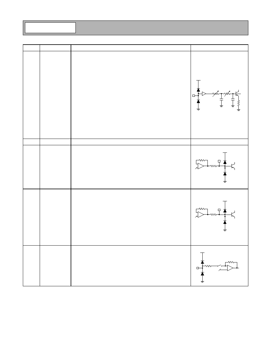
1
VCC2
Supply for LO buffers, frequency doubler and dividers.
2
LO HB P
High band local oscillator input (1800MHz).
In "low band F
LO
/2" modes the signal (LOHBP-LOHBN) undergoes a
frequency division of 2 to provide the low band LO signal for the modu-
lator.
In "high band F
LO
x1" modes the signal (LOHBP-LOHBN) is used as
the high band LO signal for the modulator.
In "high band bypass" a modulated DCS1800/PCS1900 signal
(LOHBP-LOHBN) is switched into the RF signal path. The modulator
is disabled and the signal is routed to the RFOutHb outputs through a
differential PA driver amplifier.
The LOHBP input is AC-coupled internally.
The noise performance, carrier suppression at low output powers and
sideband suppression all vary with LO power. The optimum LO power
is between -3dBm and +3dBm. The device will work with LO powers as
low as -20dBm however this is at the expense of higher phase noise in
the LO circuitry and poorer sideband suppression.
The input impedance should be externally matched to 50
. The port
can be driven either differentially or single ended. The port impedance
does not vary significantly between active and power down modes.
The RF2705 is intended for use with the RF6002. This performs the
GSM GMSK modulation within a Frac-N synthesizer loop. The 8PSK
EDGE and W-CDMA signal modulations are performed in the RF2705
and uses the RF6002's synthesizers to generate the LO signals. The
LO signal for EDGE900 mode is derived by frequency division by 2 of
the RF6002's DCS1800 VCO. This helps protect the system against PA
pulling.
3
LO HB N
The complementary LO input for both LOHBP LO signals.
In any of the modes the LOHB input may be driven either single ended
or differentially. If the LO is driven single ended then the PCB board
designer can ground this pin.
It is recommended that if this pin is grounded that it is kept isolated
from the GND1 pin and the die flag ground. All connections to any other
ground should be made through a ground plane. Poor routing of this
ground signal can significantly degrade the LO leakage performance.
See pin 2.
Modulator and
VGA
VCC2
LO HB P
LO HB N
V
CC

5-125
RF2705
Rev A4 041026
Pin
Function
Description
Interface Schematic
4
LO LB P
Low band local oscillator input (900MHz).
In "wideband F
LO
x2" and "high band F
LO
x2" modes the signal
(LOLBP-LOLBN) is doubled in frequency to provide the LO signal for
the modulator.
In "Low band F
LO
x1" modes the signal (LOLBP-LOLBN) is used as
the LO signal for the modulator.
In "Low band Bypass" a modulated GSM900 signal (LOLBP-LOLBN)
is switched into the RF signal path. The modulator is disabled and the
signal is routed to the RFOutLb outputs through a differential PA driver
amplifier.
This LOLBP input is AC-coupled internally.
The noise performance, carrier suppression at low output powers and
sideband suppression performance are functions of LO power. The
optimum LO power is between -3dBm and +3dBm. The device will
work with LO powers as low as -20dBm however this is at the expense
of higher noise performance at high output powers and poorer side-
band suppression.
The input impedance should be externally matched to 50
. The port
impedance does not vary significantly between active and powered
modes.
The RF2705 is intended for use with the RF6002 which performs the
GSM GMSK modulation within a Frac-N synthesizer loop. The 8PSK
EDGE and W-CDMA signal modulations are performed in the RF2705
and uses the RF6002's synthesizers to generate the LO signals. The
LO signal for DCS1800 mode is derived by frequency doubling
RF6002's GSM900 VCO. This helps protect the system against PA pull-
ing.
5
LO LB N
The complementary LO input for both LOLBP LO signals.
In any of the modes the LOLB input may be driven either single ended
or differentially. If the LO is driven single ended then the PCB board
designer can ground this pin.
It is recommended that if this pin is grounded that it is kept isolated
from the GND1 pin and the die flag ground. All connections to any other
ground should be made through a ground plane. Poor routing of this
GndLO signal can significantly degrade the LO leakage performance.
See pin 4.
6
MODE C
Chip enable control pin. See the Logic Truth table.
CMOS Logic inputs: Logic 0=0V to 0.4V; Logic 1=1.4V to V
CC
.
7
MODE D
Mode control pin. See the Logic Truth table.
CMOS Logic inputs: Logic 0=0V to 0.4V; Logic 1=1.4V to V
CC
.
See pin 6.
LO LB P
LO LB N
V
CC
V
CC2

5-126
RF2705
Rev A4 041026
Pin
Function
Description
Interface Schematic
8
Q SIG N
Quadrature Q channel negative baseband input port.
Best performance is achieved when the QSIGP and QSIGN are driven
differentially with a 1.2V common mode DC voltage. The recom-
mended differential drive level (V
QSIGP
-V
QSIGN
) is 1.2V
P-P
for EDGE,
0.8V
P-P
for W-CDMA modulation and 1.0V
P-P
for GMSK modulation.
This input should be DC-biased at 1.2V. In sleep mode an internal FET
switch is opened, the input goes high impedance and the modulator is
de-biased.
Phase or amplitude errors between the QSIGP and QSIGN signals will
result in a common-mode signal which may result in an increase in the
even order distortion of the modulation in the output spectrum.
DC offsets between the QSIGP and QSIGN signals will result in
increased carrier leakage. Small DC offsets may be deliberately
applied between the ISIGP/ISIGN and QSIGP/QSIGN inputs to can-
cel out the LO leakage. The optimum corrective DC offsets will change
with mode, frequency and gain control.
Common-mode noise on the QSIGP and QSIGN should be kept low
as it may degrade the noise performance of the modulator.
Phase offsets from quadrature between the I and Q baseband signals
results in degraded sideband suppression.
9
Q SIG P
Quadrature Q channel negative baseband input port. See pin 8.
See pin 8.
10
VREF
Voltage reference decouple.
External 10nF decoupling capacitor to ground.
The voltage on this pin is typically 1.67V when the chip is enabled. The
voltage is 0V when the chip is powered down.
The purpose of this decoupling capacitor is to filter out low frequency
noise (20MHz) on the gain control lines.
Poor positioning of the VREF decoupling capacitor can cause a degra-
dation in LO leakage.
A voltage of around 2.5V on this pin indicates that the die flag under
the chip is not grounded and the chip is not biased correctly.
11
GC DEC
Gain control voltage decouple with an external 1nF decoupling capaci-
tor to ground.
The voltage on this pin is a function of gain control (GC) voltage when
the chip is enabled. The voltage is 0V when the chip is powered down.
The purpose of this decoupling capacitor is to filter out low frequency
noise (20MHz) on the gain control lines. The size capacitor on the GC
DEC line will effect the settling time response to a step in gain control
voltage. A 1nF capacitor equates to around 200ns settling time and a
0.5nF capacitor equates to a 100ns settling time. There is a trade-off
between settling time and noise contributions by the gain control cir-
cuitry as gain control is applied.
Poor positioning of the VREF decoupling capacitor can cause a degra-
dation in LO leakage.
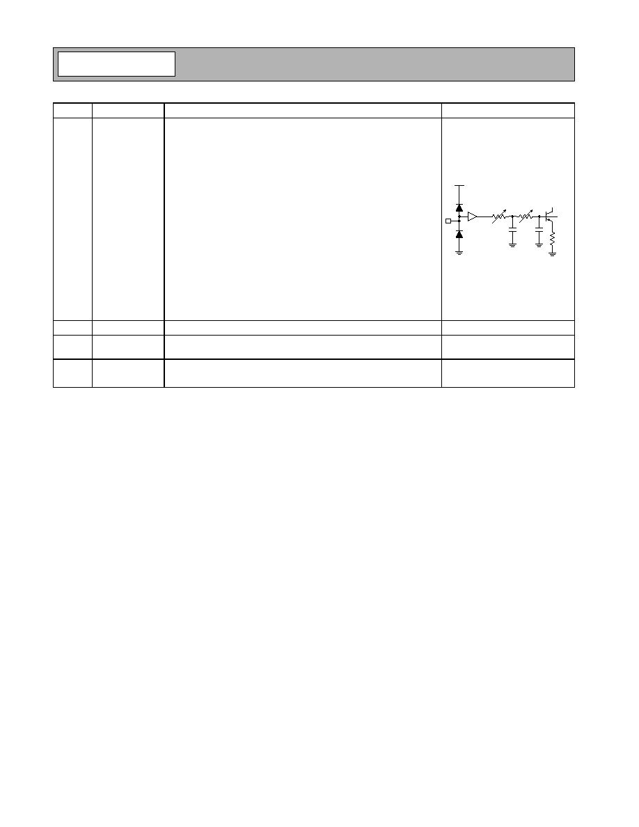
12
GC
Gain control voltage. Maximum output power at 2.0V. Minimum output
power at 0V. When the chip is enabled the input impedance is 10k
to
1.67V
DC
. When the chip is powered down a FET switch is opened and
the input goes high impedance.
V
CC2
x1
V
CC2
-
+
4 k
V
CC2
-
+
4 k
V
CC2
-
+
4 k
10 k
1.7 V

5-127
RF2705
Rev A4 041026
Pin
Function
Description
Interface Schematic
13
RF OUT
LB N
Differential low band PA driver amplifier output.
This output is intended for low band (GSM850/900) operation and
drives a differential SAW.
A bypass mode allows the low band PA driver amplifier's input to be
switched between the signal from the modulator and the signal applied
at LOLB. This enables a GMSK-modulated signal on the LOLB input to
be switched into the RF signal path.
The output is an open collector. The outputs are matched off-chip.
14
RF OUT
LB P
Complementary differential low band PA driver amplifier output.
See pin 13.
See pin 13.
15
RF OUT
HB N
Differential high band PA Driver amplifier output.
This output is intended for DCS1800/PCS1900 band operation.
A bypass mode allows the high band PA driver amplifier's input to be
switched between the signal from the modulator and the signal applied
at LOHB. This enables a GMSK-modulated DCS1800/PCS1900 signal
on the LOHB input to be switched into the RF signal path.
The output is an open collector. The outputs are matched off-chip.
16
RF OUT
HB P
Complementary differential high band PA driver amplifier output.
See pin 15.
See pin 15.
17
RF OUT
WB N
Differential high band PA driver amplifier output.
This output is intended for wide band (W-CDMA) applications.
The output is an open collector. The output are matched off-chip.
18
RF OUT
WB P
Complementary differential wideband PA driver amplifier output.
See pin 17.
See pin 17.
19
GND
Ground.
20
MODE A
Mode control pin. See the Logic Truth table.
CMOS Logic inputs: Logic 0=0V to 0.4V; Logic 1=1.4V to V
CC
.
See pin 6.
21
VCC1
Supply for modulator, VGA and PA driver amplifiers.
V
CC
V
CC
RF OUT LB N
RF OUT LB P
V
CC
V
CC
V
CC
RF OUT HB N
RF OUT HB P
V
CC
V
CC
V
CC
RF OUT WB N
RF OUT WB P
V
CC
LO Quadrature
Generator and
Buffers
VCC1
GND1

5-128
RF2705
Rev A4 041026
Pin
Function
Description
Interface Schematic
22
I SIG P
In-phase I channel positive baseband input port.
Best performance is achieved when the ISIGP and ISIGN are driven
differentially with a 1.2V common mode DC voltage. The recom-
mended differential drive level (V
ISIGP
-V
ISIGN
) is 1.2V
P-P
for EDGE,
0.8V
P-P
W-CDMA modulation and 1.0V
P-P
for GMSK modulation.
This input should be DC-biased at 1.2V. In sleep mode an internal FET
switch is opened, the input goes high impedance and the modulator is
de-biased.
Phase or amplitude errors between the ISIGP and ISIGN signals will
result in a common-mode signal which may result in an increase in the
even order distortion of the modulation in the output spectrum.
DC offsets between the ISIGP and ISIGN signals will result in
increased carrier leakage. Small DC offsets may be deliberately
applied between the ISIGP/ISIGN and QSIGP/QSIGN inputs to can-
cel out the LO leakage. The optimum corrective DC offsets will change
with mode, frequency and gain control.
Common-mode noise on the ISIGP and ISIGN should be kept low as it
may degrade the noise performance of the modulator.
Phase offsets from quadrature between the I and Q baseband signals
results in degrades sideband suppression.
23
I SIG N
In-phase I channel negative baseband input port. See pin 22.
See pin 22.
24
MODE B
Mode control pin. See the Logic Truth table.
CMOS Logic inputs: Logic 0=0V to 0.4V; Logic 1=1.4V to V
CC
.
See pin 6.
Pkg
Base
DIE FLAG
Ground for LO section, modular, biasing, variable gain amplifier, and
substrate.
V
CC2
x1

5-129
RF2705
Rev A4 041026
LO Frequency Planning Options for European 3GPP W-CDMA/EDGE
Recommended Frequency Plan: Frequency Doubler/Divide by 2/GMSK Modulator Bypass Modes
On Frequency LO with GMSK Modulator Bypass Modes
Output Frequency Band
Modulation
Format
LO Port
LO Frequency Range
Comments
Band
Lower Limit Upper Limit
Lower Limit Upper Limit
GSM850
824MHz
849MHz
EDGE 8PSK
LOHB
1648MHz
1698MHz
F
LO
/2
Divide by 2
GSM850
824MHz
849MHz
GSM GMSK
LOLB
824MHz
849MHz
F
LO
_bypass Bypass,
GMSK-modulated LO
GSM900
880MHz
915MHz
EDGE 8PSK
LOHB
1760MHz
1830MHz
F
LO
/2
Divide by 2
GSM900
880MHz
915MHz
GSM GMSK
LOLB
880MHz
915MHz
F
LO
_bypass Bypass,
GMSK-modulated LO
DCS1800
1710MHz
1785MHz
EDGE 8PSK
LOLB
855MHz
892.5MHz
F
LO
x2
Frequency Doubler
DCS1800
1710MHz
1785MHz
GSM GMSK
LOHB
1710MHz
1785MHz
F
LO
_bypass Bypass,
GMSK-modulated LO
PCS1900
1850MHz
1910MHz
EDGE 8PSK
LOLB
925MHz
955MHz
F
LO
x2
Frequency Doubler
PCS1900
1850MHz
1910MHz
GSM GMSK
LOHB
1850MHz
1910MHz
F
LO
_bypass Bypass,
GMSK-modulated LO
W-CDMA1950
1920MHz
1980MHz 3GPP W-CDMA
LOLB
960MHz
990MHz
F
LO
x2
Frequency Doubler
Output Frequency Band
Modulation
Format
LO Port
LO Frequency Range
Comments
Band
Lower Limit Upper Limit
Lower Limit Upper Limit
GSM850
824MHz
849MHz
EDGE 8PSK
LOLB
824MHz
849MHz
F
LO
x1
On Frequency
GSM850
824MHz
849MHz
GSM GMSK
LOLB
824MHz
849MHz
F
LO
_bypass Bypass,
GMSK-modulated LO
GSM900
880MHz
915MHz
EDGE 8PSK
LOLB
880MHz
915MHz
F
LO
x1
On Frequency
GSM900
880MHz
915MHz
GSM GMSK
LOLB
880MHz
915MHz
F
LO
_bypass Bypass,
GMSK-modulated LO
DCS1800
1710MHz
1785MHz
EDGE 8PSK
LOHB
1710MHz
1785MHz
F
LO
x1
On Frequency
DCS1800
1710MHz
1785MHz
GSM GMSK
LOHB
1710MHz
1785MHz
F
LO
_bypass Bypass,
GMSK-modulated LO
PCS1900
1850MHz
1910MHz
EDGE 8PSK
LOHB
1850MHz
1910MHz
F
LO
x1
On Frequency
PCS1900
1850MHz
1910MHz
GSM GMSK
LOHB
1850MHz
1910MHz
F
LO
_bypass Bypass,
GMSK-modulated LO
W-CDMA1950
1920MHz
1980MHz 3GPP W-CDMA
LOHB
1920MHz
1980MHz
F
LO
x1
On Frequency

5-130
RF2705
Rev A4 041026
Control Logic Truth Table
Mode Description
Input Logic
Active RF
I/Os
Comment
Mode A Mode B Mode C Mode D
Expected Mode of
Operation
Sleep Mode
Sleep
X
0
0
0
Sleep
Frequency Doubler/Divide by 2 Options
Wideband F
LO
x2 (High Power)
Modulator and frequency doubler
enabled
1
0
1
0
LoLbP LoLbN
RFOutWb P
RFOutWb N
Bands: 1920MHz to 1980MHz
Modulation: 3GPP W-CDMA
Wideband F
LO
x2 (Medium Power)
Modulator and frequency doubler
enabled
1
0
1
1
LoLbP LoLbN
RFOutWb P
RFOutWb N
Bands: 1920MHz to 1980MHz
Modulation: 3GPP W-CDMA
Wideband F
LO
x2 (Low Power)
Modulator and frequency doubler
enabled
1
0
0
1
LoLbP LoLbN
RFOutWb P
RFOutWb N
Bands: 1920MHz to 1980MHz
Modulation: 3GPP W-CDMA
High Band F
LO
x2
Modulator and frequency doubler
enabled
1
1
1
1
LoLbP LoLbN
RFOutHb P
RFOutHb N
Bands: DCS1800 or PCS1900
Modulation: GMSK, TDMA and
8PSK EDGE
Low Band F
LO
/2
Modulator and divide by 2 enabled
1
1
0
1
LoHbP LoHbN
RFOutLb P
RFOutLb N
Bands: GSM900 or GSM850
Modulation: GMSK, TDMA and
8PSK EDGE
GMSK Modulator Bypass Options
Low Band Bypass
Modulator bypass enabled
X
1
0
0
LoLbP LoLbN
RFOutLb P
RFOutLb N
Bands: GSM850 or GSM900
Modulation: GMSK
High Band Bypass
Modulator bypass enabled
X
1
1
0
LoHbP LoHbN
RFOutHb P
RFOutHb N
Bands: DCS1800 or PCS1900
Modulation: GMSK
On-Frequency LO Options
Wideband F
LO
x1 (High Power)
Modulator and on-frequency LO
enabled
0
0
1
0
LoHbP LoHbN
RFOutWb P
RFOutWb N
Bands: 1920MHz to 1980MHz
Modulation: 3GPP W-CDMA
Wideband F
LO
x1 (Medium Power)
Modulator and on-frequency LO
enabled
0
0
1
1
LoHbP LoHbN
RFOutWb P
RFOutWb N
Bands: 1920MHz to 1980MHz
Modulation: 3GPP W-CDMA
Wideband F
LO
x1 (Low Power)
Modulator and on-frequency LO
enabled
0
0
0
1
LoHbP LoHbN
RFOutWb P
RFOutWb N
Bands: 1920MHz to 1980MHz
Modulation: 3GPP W-CDMA
High Band F
LO
x1
Modulator and on-frequency LO
enabled
0
1
1
1
LoHbP LoHbN
RFOutHb P
RFOutHb N
Bands: DCS1800 or PCS1900
Modulation: GMSK, TDMA and
8PSK EDGE
Low Band F
LO
x1
Modulator and on-frequency LO
enabled
0
1
0
1
LoLbP LoLbN
RFOutLb P
RFOutLb N
Bands: GSM900 to GSM850
Modulation: GMSK, TDMA and
8PSK EDGE

5-131
RF2705
Rev A4 041026
Application Information
The baseband inputs of the RF2705 must be driven with balanced signals. Amplitude and phase matching <0.5dB and
<0.5 degrees are recommended. Phase or gain imbalances between the complementary input signals will cause addi-
tional distortion including some second order baseband distortion.
The RF2705 is designed to be driven with either single-ended or differential LO signals. Driving the chip differentially is
beneficial in improving the LO leakage performance. Decreasing the LO drive level will also improve LO leakage, but the
output noise performance will be degraded. Driving the LO level too high will degrade linearity.
The ground lines for the LO sections are brought out of the chip independently from the ground to the RF and modulator
sections. This is intended to give the board design the independence of isolating the LO signals from the RF output sec-
tions.
The RF2705 includes frequency doubler and divider modes that allow the LO to operate at half or twice the frequency
depending on the application. This provides some flexibility in improving VCO isolation and LO leakage through fre-
quency translation.
The RF outputs use open collector architecture and may be biased at voltages higher than V
CC
. In practice, biasing at a
higher voltage may improve the intermodulation performance. The load resistors are selected to provide sufficient output
power while maintaining good linearity.
The GC DEC and V
REF
output pins should be decoupled to ground. A 10nF capacitor on V
REF
and a 1nF capacitor on
GC CEC are recommended. The purpose of these capacitors is to filter out low frequency noise (20MHz) in the gain
control lines that may cause noise on the RF signal. The capacitor on the GC DEC line will effect the settling time of the
step response in power control voltage. A 1nF capacitor equates to around a 200ns settling time; a 0.5nF capacitor
equates to a 100ns settling time. There is a trade-off between setting time and phase noise as gain control is applied.
As with any RF circuit, the RF2705 is sensitive to PC board layout. The suggested schematic and board layout is
included as a guideline. Proper grounding of the die flag under the chip is essential in achieving acceptable RF perfor-
mance. A symmetric output structure will maintain signal balance while keeping the RF lines short will reduce losses.
Proper routing and bypassing of the supply lines will improve stability and performance, especially under low gain control
settings where carrier suppression becomes crucial. The location and value of the bypass capacitor on pin 1 is critical in
promoting good carrier suppression and is designated to resonate out the series wire bond and PC board inductance.

5-132
RF2705
Rev A4 041026
Application Schematic
7
6
5
4
3
2
1
12
11
10
9
8
18
17
16
15
14
13
23
22
21
20
19
24
Note: The die flag is the
chip's main ground.
+45∞
-45∞
DIV
2
+45∞
-45∞
Flo
x2
Mode Control
and Biasing
Power
Control
5.6 pF
V
CC
3.9 nH
LO HB
3 pF
22.0 nH
LO LB
MODE C
MODE D
Q SIG N
Q SIG P
GC
10 nF
1 nF
MODE B
I SIG N
I SIG P
1 nF
V
CC
12 nH
3.3 pF
V
CC
0.5 pF
1 k
3.3 pF
12 nH
RF OUT LB
4.3 nH
1.6 pF
V
CC
430
1.6 pF
V
CC
RF OUT HB
4.3 pF
V
CC
1 pF
1 k
4.3 pF
2.2 nH
RF OUT WB
MODE A
V
CC
V
CC
1.8 pF
2:1
T3
2:1
T1
2:1
T2
430
4.3 nH
2.2 nH

5-133
RF2705
Rev A4 041026
Evaluation Board Schematic
7
6
5
4
3
2
1
12
11
10
9
8
18
17
16
15
14
13
23
22
21
20
19
24
Note: The die flag is the
chip's main ground.
+45∞
-45∞
DIV
2
+45∞
-45∞
Flo
x2
Mode Control
and Biasing
Power
Control
C6
5.6 pF
MODE B
MODE A
C1
1 nF
VCC
50
µ
strip
J1
I SIG N
50
µ
strip
J2
I SIG P
C4
1.8 pF
L1
3.9 nH
50
µ
strip
J3
HB LO
C13
3 pF
L6
22 nH
50
µ
strip
J6
LB LO
MODE C
MODE D
50
µ
strip
J8
Q SIG N
50
µ
strip
J9
Q SIG P
C15
1 nF
C14
10 nF
P1
1
2
3
4
CON4
P2-1
MODE D
P2-4
MODE A
P2-3
MODE B
P2-2
MODE C
GC
L7
12 nH
C17
3.3 pF
R4
1 k
L8
12 nH
C16
3.3 pF
C8
100 pF
C18
0.5 pF
VCC
50
µ
strip
J7
LB RF OUT
L4
4.3 nH
C9
1.6 pF
R3
430
L5
4.3 nH
C10
1.6 pF
C11
22 pF
C5
DNI
VCC
50
µ
strip
J5
HB RF OUT
L2
2.2 nH
C2
4.3 pF
R1
1 k
L3
2.2 nH
C3
4.3 pF
C7
12 pF
C12
1.3 pF
VCC
50
µ
strip
J4
WB RF OUT
IN
I
N
GN
D
G
ND
GN
D
O
UT
T2
Murata
LDB211G8020C-001
43
5
1
6
2
T1
Murata
LDB211G9020C-001
2
5
6
4
3
1
IN
I
N
GN
D
G
N
D
GN
D
O
U
T
IN
IN
GND
G
ND
GND
O
U
T
T3
Murata
LDB21906M20C-001
43
5
1
6
2
R2
430
GND
VCC
P1-1
GC
P1-3
P2
1
2
3
CON3

5-134
RF2705
Rev A4 041026
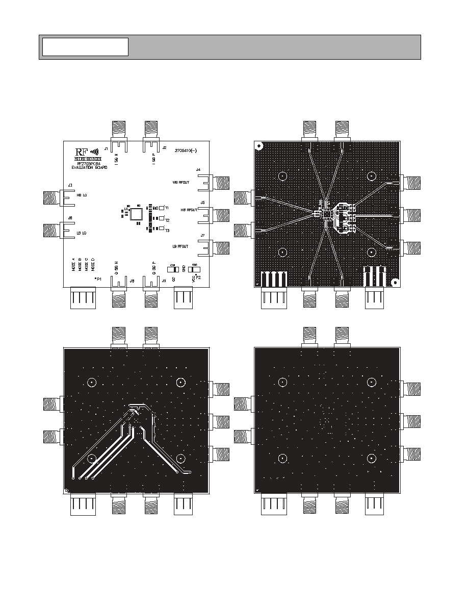
Evaluation Board Layout
Board Size 2.250" x 2.250"
Board Thickness 0.032", Board Material FR-4, Multi-Layer
Assembly
Top
Mid
Back

5-135
RF2705
Rev A4 041026
PCB Design Requirements
PCB Surface Finish
The PCB surface finish used for RFMD's qualification process is Electroless Nickel, immersion Gold. Typical thickness is
3
µ
inch to 8
µ
inch Gold over 180
µ
inch Nickel.
PCB Land Pattern Recommendation
PCB land patterns are based on IPC-SM-782 standards when possible. The pad pattern shown has been developed and
tested for optimized assembly at RFMD; however, it may require some modifications to address company specific
assembly processes. The PCB land pattern has been developed to accommodate lead and package tolerances.
PCB Metal Land Pattern
A = 0.69 x 0.28 (mm) Typ.
B = 0.28 x 0.69 (mm) Typ.
C = 2.50 (mm) Sq.
0.50 (mm) Typ.
0.50 (mm) Typ.
2.50 (mm)
Typ.
0.57 (mm) Typ.
1.25 (mm)
Typ.
0.57 (mm) Typ.
2.50 (mm)
Typ.
1.25 (mm)
Typ.
Pin 1
Pin 12
Pin 18
Pin 24
B
B
B
B
B
B
C
A
A
A
A
A
A
A
A
A
A
A
A
B
B
B
B
B
B
Figure 1. PCB Metal Land Pattern (Top View)

5-136
RF2705
Rev A4 041026
PCB Solder Mask Pattern
Liquid Photo-Imageable (LPI) solder mask is recommended. The solder mask footprint will match what is shown for the
PCB Metal Land Pattern with a 2mil to 3mil expansion to accommodate solder mask registration clearance around all
pads. The center-grounding pad shall also have a solder mask clearance. Expansion of the pads to create solder mask
clearance can be provided in the master data or requested from the PCB fabrication supplier.
Thermal Pad and Via Design
The PCB land pattern has been designed with a thermal pad that matches the exposed die paddle size on the bottom of
the device.
Thermal vias are required in the PCB layout to effectively conduct heat away from the package. The via pattern shown
has been designed to address thermal, power dissipation and electrical requirements of the device as well as accommo-
dating routing strategies.
The via pattern used for the RFMD qualification is based on thru-hole vias with 0.203mm to 0.330mm finished hole size
on a 0.5mm to 1.2mm grid pattern with 0.025mm plating on via walls. If micro vias are used in a design, it is suggested
that the quantity of vias be increased by a 4:1 ratio to achieve similar results.
0.50 (mm) Typ.
0.50 (mm) Typ.
2.50 (mm)
Typ.
0.57 (mm) Typ.
1.25 (mm)
Typ.
0.57 (mm) Typ.
2.50 (mm)
Typ.
1.25 (mm)
Typ.
Pin 1
Pin 12
Pin 18
Pin 24
B
B
B
B
B
B
C
A
A
A
A
A
A
A
A
A
A
A
A
B
B
B
B
B
B
A = 0.79 x 0.38 (mm) Typ.
B = 0.38 x 0.79 (mm) Typ.
C = 2.60 (mm) Sq.
Figure 2. PCB Solder Mask Pattern (Top View)
