 | –≠–ª–µ–∫—Ç—Ä–æ–Ω–Ω—ã–π –∫–æ–º–ø–æ–Ω–µ–Ω—Ç: RF2890 | –°–∫–∞—á–∞—Ç—å:  PDF PDF  ZIP ZIP |

8-409
Product Description
Ordering Information
Typical Applications
Features
Functional Block Diagram
RF Micro Devices, Inc.
7628 Thorndike Road
Greensboro, NC 27409, USA
Tel (336) 664 1233
Fax (336) 664 0454
http://www.rfmd.com
Optimum Technology MatchingÆ Applied
Si BJT
GaAs MESFET
GaAs HBT
Si Bi-CMOS
SiGe HBT
Si CMOS
InGaP/HBT
GaN HEMT
SiGe Bi-CMOS
CELL
LNA IN
CELL
LNA EMITTER
CELL
LNA OUT
ISE
T
1
GPS
LNA IN
VG1
GPS
LNA OUT
VCC2
IS
E
T
2
CELL MIX IN
NC
DIV SEL
ENABLE
LO OUT
TX BUFF
ENAB
CDMA IF-
CDMA IF+
GPS IF-
GPS IF+
GPS
MIX IN
VG2
BAND SE
L
VCC1
LO
IN
1
3
2
6
24
23
22
21
20
19
4
5
12
18
15
17
16
14
13
10
9
7
8
11
/2
RF2890
DUAL-BAND CDMA CELLULAR/GPS
LOW NOISE AMPLIFIER/MIXER
∑ CDMA Cellular/GPS Applications
∑ JCDMA/GPS Applications
∑ AMPS/GPS Applications
∑ CDMA Modem/Data Cards
∑ Commercial and Consumer Systems
∑ Portable Battery-Powered Equipment
The RF2890 is a high performance dual band CDMA Cel-
lular and GPS LNA/mixer. An integrated optional LO pres-
caler allows VCO flexibility. The device is designed to
exceed all sensitivity, intermodulation and single-tone
requirements. The RF2890 is designed for three state
gain control solutions (17.5dB of gain control) for cellular
band IMD testing. The device offers a dedicated low cur-
rent (15.5mA) GPS LNA/mixer with 32.5dB gain. An inte-
grated TX LO buffer is also included. The design is
flexible, in that the bias currents may be set using off-chip
current reference resistors for the mixer and LNA blocks.
Noise figure, IIP3, and other specifications are designed
to be compatible with the TIA/EIA 98D standard for
CDMA cellular communications. The device is packaged
in a plastic, 4mmx4mm QFN.
∑ Optional Divide-by-Two LO Prescaler
allows VCO Flexibility
∑ Three Gain State Cellular LNA
∑ High IIP3 (8.5dBm) Cellular Mixer
∑ Full ESD Protection on all Pins
∑ 15.5mA GPS LNA/Mixer Solution
RF2890
Dual-Band CDMA Cellular/GPS Low Noise
Amplifier/Mixer
RF2890PCBA-410
Fully Assembled Evaluation Board
0
Rev A4 040421
Dimensions in mm
0.05 C
SEATING
PLANE
12∞
MAX
-C-
0.05
0.00
0.70
0.65
0.90
0.85
Top View
-A-
3
1.87 TYP
3.75 SQ
0.15 C A
2 PLCS
-B-
4.00 SQ
2.00 TYP
0.15 C B
2 PLCS
0.15 C A
2 PLCS
0.15 C B
2 PLCS
NOTES:
1 Shaded lead is pin 1.
Dimension applies to plated terminal: to be measured between 0.20 mm and 0.25 mm from terminal end.
Pin 1 identifier must exist on top surface of package by identification mark or feature on the package body.
2
3
0.50
0.30
TYP
PIN 1 ID
0.20 R
0.60
0.24
TYP
C
0.10 M
A B
2
0.30
0.18
0.50
Bottom View
2.49
2.19
SQ.
Package Style: QFN, 24-Pin, 4x4

8-410
RF2890
Rev A4 040421
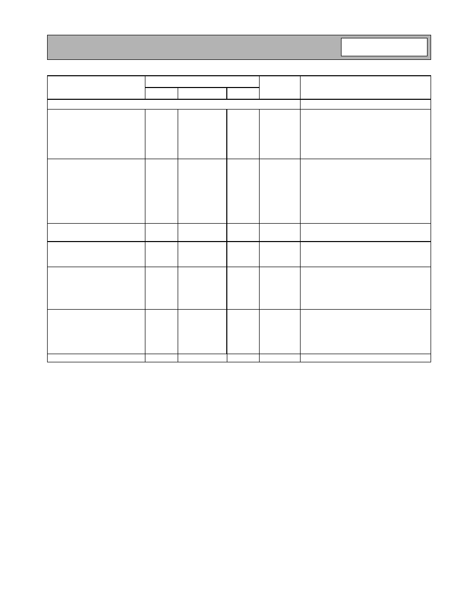
Absolute Maximum Ratings
Parameter
Rating
Unit
Supply Voltage
-0.5 to +5.0
V
DC
Input LO and RF Levels
+6
dBm
Operating Ambient Temperature
-40 to +85
∞C
Storage Temperature
-40 to +150
∞C
Parameter
Specification
Unit
Condition
Min.
Typ.
Max.
Overall
T = 25∞C, V
CC
=2.75V
RF Frequency Range
800 to 900
MHz
Cellular band
1575.42
MHz
GPS band
IF Frequency Range
0.1
183.6
400
MHz
Power Supply
Supply Voltage
2.65
2.75
3.15
V
Logic High
1.8
V
Logic Low
0.4
V
Power Down Current
10
µ
A
ENABLE=0
Cellular Band
JCDMA Band
Freq=869MHz to 894MHz
Freq=832MHz to 870MHz
LNA (High Gain)
LNA 50
match
Gain
13.0
14.5
16.0
dB
Noise Figure
1.0
1.3
dB
Input IP3
+9.0
+11.0
dBm
IIP3 can be increased further by decreasing
the value of ISET1.
Current
7.0
mA
Isolation
19
dB
LNA (Mid Gain)
LNA 50
match
Gain
5.5
7.0
8.5
dB
Noise Figure
2.5
2.8
dB
Input IP3
+9.0
+12.0
dBm
Current
4.0
mA
LNA (Low Gain)
Gain
-4.0
-3.0
-1.5
dB
Noise Figure
3.0
4.0
dB
Input IP3
+20.0
+23.0
dBm
Current
0
mA
Mixer - CDMA/JCDMA
LO IN=-4dBm
See Notes 1, 2 and 3.
Gain
10.0
11.5
13.0
dB
Noise Figure
7.5
8.0
dB
Input IP3
+6.5
+8.5
dBm
Current
13.5
mA
LO Frequency Range
600
2300
MHz
High and Low Side LO Injection.
See note 3 and 4.
2105.2-2155.2
MHz
/2 enabled, 183.6MHz IF
IF Frequency Range
0.1
183.6
400
MHz
Typical IF frequencies:
111.85MHz, 183.6MHz
Cellular Mode (High Gain)
Total Current
27.5
37.0
mA
LO/2 enabled, TX LO Buffer enabled
Caution! ESD sensitive device.
RF Micro Devices believes the furnished information is correct and accurate
at the time of this printing. However, RF Micro Devices reserves the right to
make changes to its products without notice. RF Micro Devices does not
assume responsibility for the use of the described product(s).
8-411
RF2890
Rev A4 040421
Parameter
Specification
Unit
Condition
Min.
Typ.
Max.
GPS Band
Freq=1575.42MHz
LNA (High Gain)
LNA 50
match
Gain
15.0
16.5
18.0
dB
Noise Figure
1.4
1.7
dB
Input IP3
+3.5
+6.0
dBm
Current
7.0
mA
Isolation
20
dB
Mixer
LO IN=-4dBm
See note 1.
Gain
16.0
17.5
19.0
dB
Noise Figure
7.0
7.5
dB
Input IP3
-5.5
-3.0
dBm
Current
8.0
mA
Mixer/LO Input Amps
LO Frequency Range
1300
1450
MHz
Low Side LO Injection
IF Frequency Range
125
183.6
275
MHz
Typical IF frequency: 183.6MHz
GPS Mode
Total Current
15.5
20.0
mA
Control Lines
Input Capacitance
1
pF
BAND SEL, VG1, VG2, ENABLE, DIV SEL,
TX BUFF ENAB
Local Oscillator Input
Cellular - CDMA/FM/JCDMA
Input Power
-10
-4
0
dBm
GPS
Input Power
-10
-4
0
dBm
TX (Local Oscillator)
Buffer
Cellular - CDMA/FM/JCDMA
Output Power
-7.0
-4.5
-2.0
dBm
Single-ended 50
load
Output Frequency
600
1078
MHz
See note 3. High and Low Side LO Injection.
Current Consumption
2
mA
NOTE 1. Mixer performance can be changed with external IF load/tuning.
NOTE 2. Specifications apply for conditions of LO Divider enabled or disabled.
NOTE 3. Mixer performance applies to both high and low side LO injection.
8-412
RF2890
Rev A4 040421
Evaluation Board Current Measurement
NOTES:
All IDC current numbers include bias circuitry current of 1.5mA to 2.0mA (dependent on mode).
TX Buffer On (=1): Add 2mA to total current.
DIV SEL On (=0): Add 2mA to total current.
"X" denotes setting does not impact current.
Cascaded Performance (Typical Values for V
CC
=2.75V)
NOTE: All total current numbers include bias circuitry current of 1.5mA to 2.0mA (dependent on mode).
BAND
SEL ENABLE
VG1
VG2
TX BUFF
ENAB
DIV
SEL
IDC
(mA)
CDMA Cellular
ISET2=7.5k
High Gain Mode,
TX Buffer Off, /2 Off
0
1
0
0
0
1
23.5
Mid Gain Mode,
TX Buffer Off, /2 Off
0
1
1
0
0
1
20.5
Low Gain Mode,
TX Buffer Off, /2 Off
0
1
1
1
0
1
16.5
Alternate Low Gain Mode,
TX Buffer Off, /2 Off
0
1
0
1
0
1
16.5
GPS
ISET2=7.5k
GPS Mode
1
1
X
X
X
1
15.5
Parameter
CELL CDMA
HIGH GAIN
MID GAIN
LOW GAIN
Cascaded:
Gain (dB)
23.5
16.0
6.0
Noise Figure (dB)
2.0
5.5
13.0
Input IP3 (dBm)
-3.7
+3.4
+13.5
Total Current (mA)
23.5
20.5
16.5
NOTE: Assumes 2.5dB image filter insertion loss. The TX Buffer is off (TX
BUFF ENAB=0). DIV SEL function is off (=1).
Parameter
GPS
Cascaded:
Gain (dB)
32.5
Noise Figure (dB)
1.8
Input IP3 (dBm)
-18.0
Total Current (mA)
15.5
NOTE: Assumes 1.5dB image filter insertion loss.
8-413
RF2890
Rev A4 040421
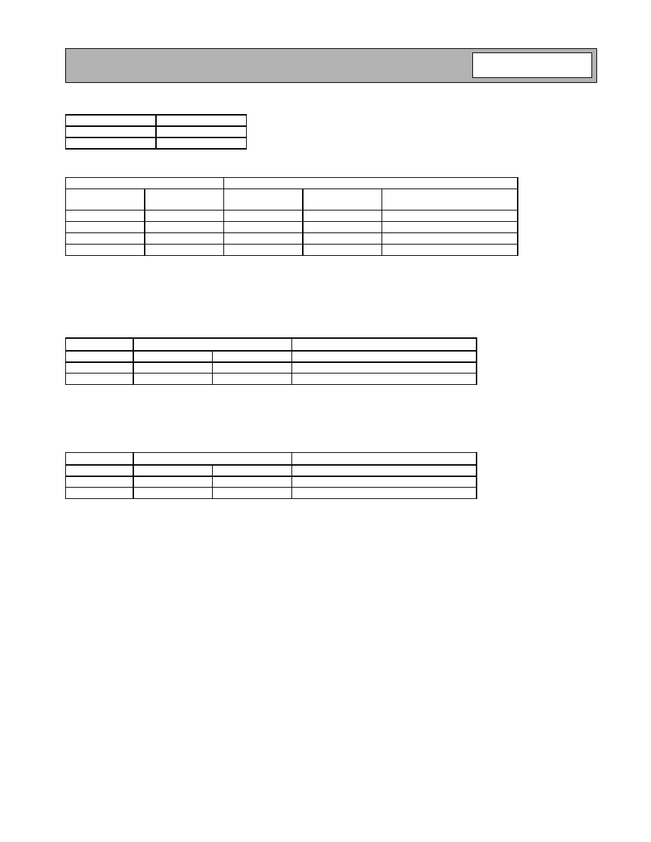
Operation Mode Control Table
Gain Control Logic Table
VCO Options and Divider Logic Table
Mode
BAND SEL
Cellular CDMA
0
GPS
1
Gain Setting
Resulting Gain State
VG1
VG2
Cellular
LNA
GPS
LNA
Comments
0
0
High Gain
High Gain
Cellular CDMA IMD Test 1 and 2
1
0
Mid Gain
High Gain
Cellular CDMA IMD Test 3 and 4
1
1
Low Gain
High Gain
Cellular CDMA IMD Test 5 and 6
0
1
Low Gain
High Gain
Cellular CDMA IMD Test 5 and 6
Dual-Band Application
Dual VCO Configuration
2GHz CDMA VCO
1.4GHz GPS VCO
DIV SEL pin tied to BAND SEL
MODE
CONTROL PINS
ON-CHIP LO PRESCALER RESULT
DIV SELECT
BAND SEL
Divide-by-2
CDMA Cellular
0
0
ON
GPS
1
1
OFF
Dual-Band Application
Dual VCO Configuration
1GHz CDMA VCO
1.4GHz GPS VCO
DIV SEL pin tied to VCC
MODE
CONTROL PINS
ON-CHIP LO PRESCALER RESULT
DIV SELECT
BAND SEL
Divide-by-2
CDMA Cellular
1
0
OFF
GPS
1
1
OFF

8-414
RF2890
Rev A4 040421
Pin
Function
Type Description
Interface Schematic
1
CELL LNA
OUT
AO
Cellular LNA output. Simple external L-C components
required for matching and VCC supply.
See pin 3.
2
CELL LNA
EMITTER
AO
Cellular LNA emitter. A small inductor connects this pin to
ground. Cellular LNA gain can be adjusted by the inductance.
See pin 3.
3
CELL LNA
IN
AI
Cellular LNA input.
4
GPS LNA IN
AI
GPS LNA input. For best performance, simple external match-
ing required.
5
VG1
DI
Logic input. See Gain Control Logic table.
6
GPS LNA
OUT
AO
GPS LNA output. Simple external L-C components required
for matching and VCC supply.
See pin 4.
7
GPS MIX IN
AI
GPS mixer RF single-end input. Externally matched to 50
.
8
VG2
DI
Logic input. See Gain Control Logic table.
9
BAND SEL
DI
Logic input. High level selects GPS band; low level selects cel-
lular band.
10
VCC1
P
VCC connection with internal RF bypass capacitor. External
bypass capacitor between 1nF and 47nF recommended.
11
LO IN
AI
LO single-end input. Matched to 50
.
12
VCC2
DI
VCC connection with internal RF Bypass capacitor. External
bypass capacitor between 1nF and 47nF recommended.
13
LO OUT
AO
LO output. Internal DC block.
14
TX BUFF
ENAB
DI
Logic input. High enables TX LO output buffer amplifiers.
CELL LNA IN
V
CC
CELL LNA OUT
CELL LNA EMITTER
GPS LNA IN
V
CC
GPS LNA OUT
VG1
GPS MIX IN
VG2
BAND SEL
LO IN
70
TX BUFF ENAB

8-415
RF2890
Rev A4 040421
Pin
Function
Type Description
Interface Schematic
15
CDMA IF-
AO
CDMA IF output. Open collector.
See pin 16.
16
CDMA IF+
AO
CDMA IF output. Open collector.
17
GPS IF-
AO
GPS IF output. Open collector.
See pin 18.
18
GPS IF+
AO
GPS IF output. Open collector.
19
ISET2
AO
Resistor to ground sets mixer currents in both bands. Higher
resistance results in lower currents.
20
ISET1
AO
Resistor to ground sets the LNA current in boost mode (both
LNAs). Higher resistance results in lower current.
21
CELL MIX
IN
AI
Cellular mixer RF single-end input. Externally matched to 50
.
22
NC
No connection.
23
DIV SEL
DI
Logic input. Logic low enables LO divide-by-2 in cellular
mode, DIV SEL must be set high in GPS mode. See VCO
options table.
24
ENABLE
DI
Logic input. Low level powers down the IC.
Pkg
Base
GND
P
Ground connection. The backside of the package should be
soldered to a top side ground pad which is connected to the
ground plane with multiple vias.
Legend:
DI=Digital Input from Baseband Chip
AI=Analog Input
AO=Analog Output
P=V
CC
or GND
CDMA IF+
CDMA IF-
GPS IF+
GPS IF-
CELL MIX IN
DIV SEL
ENABLE

8-416
RF2890
Rev A4 040421
Application Schematic
Differential Configuration
33 nF
33 nH
33 nF
1.8 nH
1.2 pF
G1
4.7 nH
10 pF
22 nH
30
33 nF
33 nF
15 nH
TX BUFF
ENAB
ENABLE
DIV
SEL
33 nF
33 nF
33 nH
16 k
7.5 k
1
3
2
6
24
23
22
21
20
19
4
5
12
18
15
17
16
14
13
10
9
7
8
11
/2
5.6 nH
33 nF
V
CC
CELL LNA IN
DNI
GPS LNA IN
GPS
RF
SAW
G2 BAND
SEL
V
CC
V
CC1
LO IN
V
CC2
LO OUT
33 nH
CELL
RF
SAW
L1
(0603
Wire-wound
Coilcraft)
L2
(0603
Wire-wound
Coilcraft)
V
CC
R1
C1
C2
C3
L3
(0603
Wire-wound
Coilcraft)
CDMA IF
(IFSAW1)
SAW
CDMA
L4
(0603
Wire-wound
Coilcraft)
L5
(0603
Wire-wound
Coilcraft)
V
CC
R2
C4
C5
C6
L6
(0603
Wire-wound
Coilcraft)
GPS IF
(IFSAW2)
SAW
GPS
8.2 nH
10 nH
6.2 pF
0
0
IF Frequency
CDMA IF OUTPUT
184 MHz
85 MHz
C1
1.8 pF
22 pF
R1
DNI
DNI
L1
68 nH
68 nH
L2
68 nH
68 nH
C2
5.6 pF
7.5 pF
C3
5.6 pF
7.5 pF
L3
47 nH
270 nH
IF SAW1
EPCOS B4955
LG 0085G2
IF Frequency
GPS IF OUTPUT for use with SAW FILTER
184 MHz
C4
DNI
C5
5.6 pF
C6
5.6 pF
L4
180 nH
L5
180 nH
L6
47 nH
R2
10 k
IF SAW2
Murata SAFCC183MCA1
Note 1: L1, L2, and L3 may be substituted with 0402 wire-wound inductors of the same value.
Note 2: For single-ended configurations, C3 and C6 are removed.
Note 3: If system specifications allow the removal of the GPS RF SAW Filter, see diagram below for
pin 6 and pin 7 connections.
*Note 3
6
7
4.7 nH
10 pF
22 nH
30
33 nF
33 nF
15 nH
V
CC
8.2 nH

8-417
RF2890
Rev A4 040421
Application Schematic
GPS LC Filter
CDMA IF SAW Filter
33 nF
33 nH
33 nF
1.8 nH
1.2 pF
G1
4.7 nH
10 pF
22 nH
30
33 nF
33 nF
15 nH
TX BUFF
ENAB
ENABLE
DIV
SEL
33 nF
33 nF
33 nH
16 k
7.5 k
1
3
2
6
24
23
22
21
20
19
4
5
12
18
15
17
16
14
13
10
9
7
8
11
/2
5.6 nH
33 nF
V
CC
CELL LNA IN
DNI
GPS LNA IN
GPS
RF
SAW
G2 BAND
SEL
V
CC
V
CC1
LO IN
V
CC2
LO OUT
33 nH
CELL
RF
SAW
L5
(0603
Wire-wound
Coilcraft)
L6
(0603
Wire-wound
Coilcraft)
V
CC
R1
C7
C8
C9
L7
(0603
Wire-wound
Coilcraft)
CDMA IF
(IFSAW1)
SAW
CDMA
L1
(0603
Wire-wound
Coilcraft)
L2
(0603
Wire-wound
Coilcraft)
V
CC
R1
C1
C2
GPS
8.2 nH
10 nH
6.2 pF
0
0
IF Frequency
CDMA IF OUTPUT
184 MHz
85 MHz
C7
1.8 pF
22 pF
R1
DNI
DNI
L5
68 nH
68 nH
L6
68 nH
68 nH
C8
5.6 pF
7.5 pF
C9
5.6 pF
7.5 pF
L7
47 nH
270 nH
IF SAW 1
EPCOS B4955
LG LG0085G2
IF Frequency
GPS IF OUTPUT
184 MHz
C1
DNI
R1
10 k
L1
330 nH
L2
220 nH
C2
5.6 pF
C3
9 pF
L3
82 nH
C4
10 nF
C5
9 pF
L4
82 nH
C6
1 nF
C3
L3
(0603
Wire-wound
Coilcraft)
C4
C5
C6
Note 1: L3, L4, L5, L6, and L7 may be substituted with 0402 wire-wound inductors of the same value.
Note 2: For single-ended configurations, C3 and C6 are removed.
Note 3: L1 and L2 must be 0603 wire-wound inductors to achieve datasheet performance.
Note 4: If system specifications allow the removal of the GPS RF SAW Filter, see diagram below for
pin 6 and pin 7 connections.
*Note 4
6
7
4.7 nH
10 pF
22 nH
30
33 nF
33 nF
15 nH
V
CC
8.2 nH
L4
(0603
Wire-wound
Coilcraft)

8-418
RF2890
Rev A4 040421
Evaluation Board Schematic
IF Freq=183.6MHz (Cellular and GPS IF)
(Download Bill of Materials from www.rfmd.com.)
L1
8.2 nH
VCC
C14
3.3 pF
50
µ
strip
J1
CELL LNA OUT
50
µ
strip
J2
CELL LNA IN
C32
33 nF
L16
1.8 nH
C29
1.2 pF
50
µ
strip
J5
GPS LNA IN
C34
33 nF
VG1
L20
4.7 nH
C35
10 pF
L19
22 nH
R8
30
C33
33 nF
50
µ
strip
J6
GPS LNA OUT
C36
33 nF
L21
15 nH
50
µ
strip
J7
GPS MIXER IN
C38
33 nF
VG2
C40
33 nF
BAND SEL
C41
33 nF
VCC1
VCC2
50
µ
strip
J8
LO IN
50
µ
strip
J9
LO OUT
C43
33 nF
TX BUF ENAB
C8
2.7 pF
C11
6.8 pF
50
µ
strip
J11
CDMA
C18
2.7 pF
L2
110 nH
C10
33 nF
VCC
ENABLE
C16
33 nF
C17
33 nF
DIV SEL
C1
33 nF
C4
33 nF
L6
39 nH
50
µ
strip
J14
CELL MIXER IN
R4
16 k
R5
7.5 k
C20
2.0 pF
L12
270 nH
C19
2.0 pF
C26
4.3 pF
L11
150 nH
C24
33 nF
VCC
50
µ
strip
J12
GPS
1
3
2
6
24
23
22
21
20
19
4
5
12
18
15
17
16
14
13
10
9
7
8
11
/2
VCC
L9
8.2 nH
R3
7.5 k
L3
220 nH
L66
27 nH
DNI
R6
22 k
0
L22
2.2 nH
0
L4
5.6 nH
C15
24 pF
C2
33 nF
8-419
RF2890
Rev A4 040421
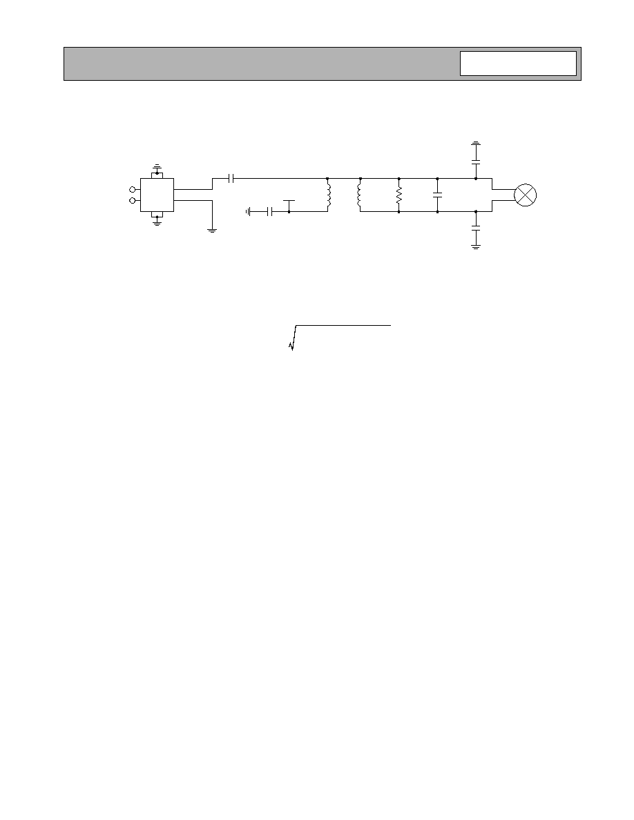
IF Output Interface Network
Single-End IF Matching
L1, C1, C2, and R form a current combiner which performs a differential to single-ended conversion at the IF frequency
and sets the output impedance. In most cases, the resonance frequency is independent of R and can be set according to
the following equation:
Where C
EQ
is the equivalent stray capacitance and capacitance looking into pins 9 and 10. An average value to use for
C
EQ
is 2.5pF.
R can then be used to set the output impedance according to the following equation:
where R
OUT
is the desired output impedance and R
P
is the parasitic equivalent parallel resistance of L1.
C
2
should first be set to 0 and C1 should be chosen as high as possible (not greater than 39pF), while maintaining an R
P
of L1 that allows for the desired R
OUT
. If the self-resonant frequencies of the selected C1 produce unsatisfactory linearity
performance, their values may be reduced and compensated for by including C2 capacitor with a value chosen to main-
tain the desired F
IF
frequency.
L2 and C3 serve dual purposes. L2 serves as an output bias choke, and C3 serves as a series DC block.
In addition, L2 and C3 may be chosen to form an impedance matching network if the input impedance of the IF filter is
not equal to R
OUT
. Otherwise, L2 is chosen to be large (suggested 120nH) and C3 is chosen to be large (suggested
22nF) if a DC path to ground is present in the IF filter, or omitted if the filter is DC-blocked.
IF-
IF+
C2
R
L1
L2
V
CC
100 pF
C3
IF Saw
4
5
9
10
IF+
IF-
C1
C1
f
IF
1
L1
2
------ C
1
2C
2
C
EQ
+
+
(
)
2
-----------------------------------------------------------
=
R
1
4 R
OUT
---------------------
1
R
P
------
≠
1
≠
=

8-420
RF2890
Rev A4 040421
Differential IF Matching
L1 and C1 are chosen to resonate at the desired IF frequency. C1 can be omitted and the value of L1 increased and uti-
lized solely as a choke to provide V
CC
to the open-collector outputs, but it is strongly recommended that at least some
small-valued C1 (a few pF) be retained for better mixer linearity performance. R is normally selected to match the input
impedance of the IF filter. However, mixer performance can be modified by selecting an R value that is different from the
IF filter input impedance, and inserting a conjugate matching network between the Resistive Output Network and the IF
filter.
C2 serve dual purposes. C2 serves as a series DC block when a DC path to ground is present in the IF filter. In addition,
C2 may be chosen to improve the combine performance of the mixer and IF filter. L2 should choose to resonate with the
internal capacitance of the SAW filter. Usually, SAW filter has some capacitance. Otherwise, L2 could be eliminated.
A practical approach to obtain the differential matching is to tune the mixer to the correct load point for gain, IIP3, and NF
using the single-end current combiner method. Second, use the component values found in the single-end approach as
starting point for the differential matching. The two-shunt capacitors in the single-end could be converted in a parallel
capacitor and the parallel inductor in the single-end need to be converted in two-choke inductor. Third, set the DC block
capacitors (C2) in the differential-end matching to a high value (i.e., 100pF) and retune the resonate circuit (C1 & L1)
and the resistor (R) for optimal performance. After optimal performance is achieved and if performance is not satisfac-
tory, decrease the series capacitors until optimal performance is achieved.
C1
R
L1
L1
V
CC
100 pF
C2
C2
IF+
IF-
L2
IF Saw
4
5
9
10
IF-
IF+
8-421
RF2890
Rev A4 040421
PCB Design Requirements
PCB Surface Finish
The PCB surface finish used for RFMD's qualification process is electroless nickel, immersion gold. Typical thickness is
3
µ
inch to 8
µ
inch gold over 180
µ
inch nickel.
PCB Land Pattern Recommendation
PCB land patterns are based on IPC-SM-782 standards when possible. The pad pattern shown has been developed and
tested for optimized assembly at RFMD; however, it may require some modifications to address company specific
assembly processes. The PCB land pattern has been developed to accommodate lead and package tolerances.
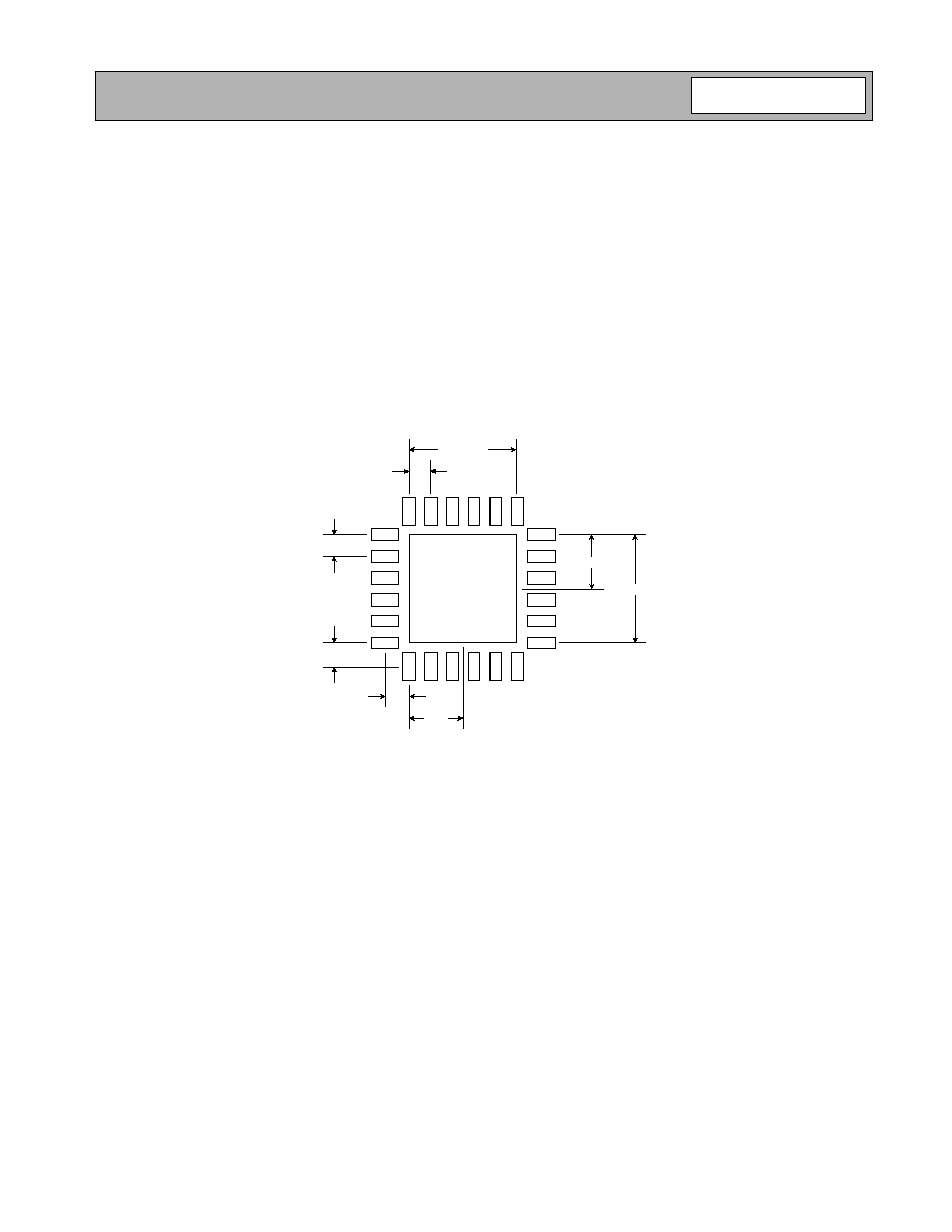
PCB Metal Land Pattern
A = 0.64 x 0.28 (mm) Typ.
B = 0.28 x 0.64 (mm) Typ.
C = 2.50 (mm) Sq.
Pin 1
Pin 18
Pin 12
Pin 24
Dimensions in mm.
A
A
A
A
A
A
B
B
B
B B
B
A
A
A
A
A
A
B
B
B
B
B
B
C
2.50 Typ.
0.50 Typ.
0.50 Typ.
0.55 Typ.
0.55 Typ.
2.50 Typ.
1.25
1.25
Figure 1. PCB Metal Land Pattern (Top View)

8-422
RF2890
Rev A4 040421