2-1
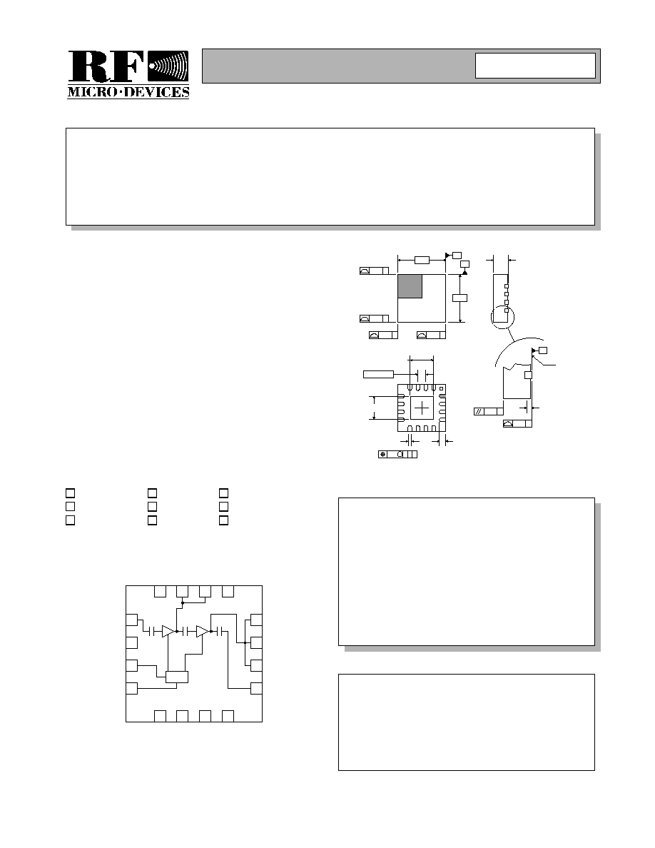
Product Description
Ordering Information
Typical Applications
Features
Functional Block Diagram
RF Micro Devices, Inc.
7628 Thorndike Road
Greensboro, NC 27409, USA
Tel (336) 664 1233
Fax (336) 664 0454
http://www.rfmd.com
Optimum Technology MatchingÆ Applied
Si BJT
GaAs MESFET
GaAs HBT
Si Bi-CMOS
SiGe HBT
Si CMOS
InGaP/HBT
GaN HEMT
SiGe Bi-CMOS
RF IN
RF OUT
NC
NC
VMODE
GND
VREG
NC
VCC2
VCC2
VCC2
NC
NC
VCC
1
IM
IM
16
15
14
13
1
2
3
4
8
7
6
5
9
10
11
12
Bias
RF3165
3V 1700MHz LINEAR POWER
AMPLIFIER MODULE
∑ 3V CDMA Korean-PCS Handset
∑ 3V CDMA2000/1XRTT K-PCS Handset
∑ 3V CDMA2000/1X-EV-DO K-PCS Handset
∑ Spread-Spectrum System
The RF3165 is a high-power, high-efficiency linear ampli-
fier module specifically designed for 3V handheld sys-
tems. The device is manufactured on an advanced third
generation GaAs HBT process, and was designed for use
as the final RF amplifier in 3V IS-95/CDMA 2000 1X
handheld digital cellular equipment, spread-spectrum
systems, and other applications in the 1750MHz to
1780MHz band. The RF3165 has a digital control line for
low power applications to lower quiescent current. The
RF3165 is assembled in at 16-pin, 3mmx3mm, QFN
package.
∑ Input Internally Matched@50
∑ Output Internally Matched
∑ 28dBm Linear Output Power
∑ 40% Peak Linear Efficiency
∑ 28dB Linear Gain
∑ -50dBc ACPR @ 1.25MHz
RF3165
3V 1700MHz Linear Power Amplifier Module
RF3165PCBA-410
Fully Assembled Evaluation Board
0
Rev A0 040730
3.00
-B-
3.00
-A-
0.10 C
0.10 C
0.10 C
0.10 C
SCALE:
NONE
SEATING
PLANE
-C-
0.05
0.00
0.08 C
0.10 C
1.00
0.80
0.50 TYP.
1.45
+0.10
-0.15
1.45
+0.10
-0.15
0.30
0.18
TYP.
0.50
0.30
TYP.
0.10
C A B
M
Shaded areas represent pin 1.
Dimensions in mm.
Package Style: QFN, 16-Pin, 3x3
Preliminary

Preliminary
2-2
RF3165
Rev A0 040730
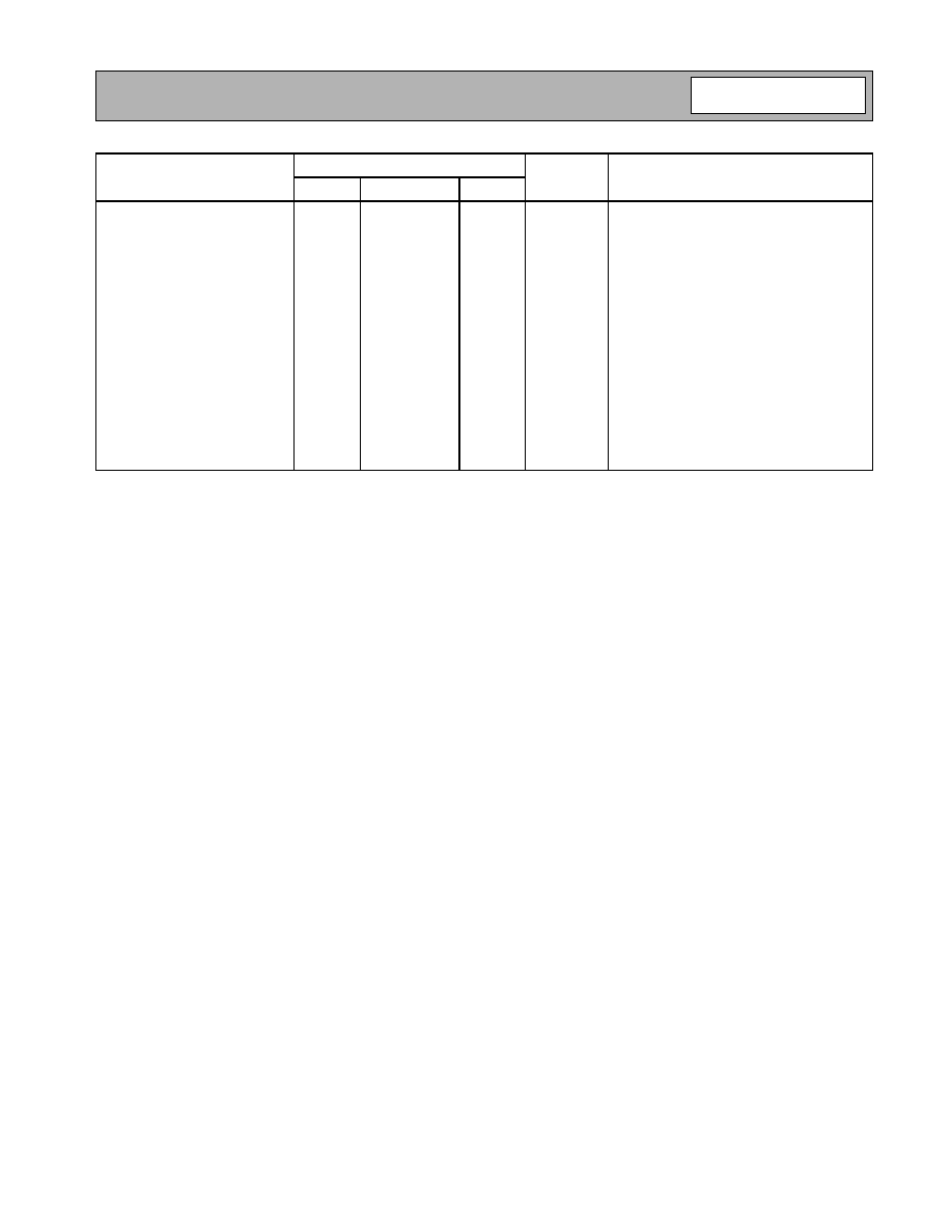
Absolute Maximum Ratings
Parameter
Rating
Unit
Supply Voltage (RF off)
+8.0
V
Supply Voltage (P
OUT
31dBm)
+5.2
V
Control Voltage (V
REG
)
+3.9
V
Input RF Power
+10
dBm
Mode Voltage (V
MODE
)
+3.9
V
Operating Temperature
-30 to +110
∞C
Storage Temperature
-40 to +150
∞C
Moisture Sensitivity Level
IPC/JEDEC J-STD-20
MSL 2 @260
∞C
Parameter
Specification
Unit
Condition
Min.
Typ.
Max.
High Gain Mode (V
MODE
Low)
T=25
o
C Ambient, V
CC
=3.4V, V
REG
=2.8V,
V
MODE
=0V, and P
OUT
=28dBm for all
parameters (unless otherwise specified).
Operating Frequency Range
1750
1780
MHz
Linear Gain
26
28
dB
Second Harmonics
-35
dBc
Third Harmonics
-40
dBc
Maximum Linear Output
28
dBm
Linear Efficiency
40
%
Maximum I
CC
460
mA
ACPR @ 1.25MHz
-50
dBc
ACPR @ 1.98MHz
-55
dBc
ACPR @ 2.25MHz
-59
dBc
Input VSWR
2:1
Output VSWR Stability
6:1
No oscillation>-70dBc
10:1
No damage
Noise Power
-138
dBm/Hz
At 90MHz offset.
Low Gain Mode (V
MODE
High)
T=25
o
C Ambient, V
CC
=3.4V, V
REG
=2.8V,
V
MODE
=2.8V, and P
OUT
=28dBm for all
parameters (unless otherwise specified).
Operating Frequency Range
1750
1780
MHz
Linear Gain
27
dB
Second Harmonics
-35
dBc
Third Harmonics
-40
dBc
Maximum Linear Output
18
28
dBm
Linear Efficiency
40
%
ACPR @1.25MHz
-50
dBc
ACPR @ 1.98MHz
-54
dBc
ACPR @2.25MHz
-58
dBc
Maximum I
CC
130
mA
P
OUT
=16dBm
Linear Gain
26
dB
P
OUT
=16dBm
Input VSWR
2:1
Output VSWR Stability
6:1
No oscillation>-70dBc
10:1
No damage
Caution! ESD sensitive device.
RF Micro Devices believes the furnished information is correct and accurate
at the time of this printing. However, RF Micro Devices reserves the right to
make changes to its products without notice. RF Micro Devices does not
assume responsibility for the use of the described product(s).
Preliminary
2-3
RF3165
Rev A0 040730
Parameter
Specification
Unit
Condition
Min.
Typ.
Max.
Power Supply
Supply Voltage
3.2
3.4
4.2
V
High Gain Idle Current
65
mA
V
MODE
=low and V
REG
=2.8V
Low Gain Idle Current
55
mA
V
MODE
=high and V
REG
=2.8V
V
REG
Current
2
mA
V
MODE
Current
250
uA
RF Turn On/Off Time
1.2
6
uS
DC Turn On/Off Time
2
40
uS
Total Current (Power Down)
0.2
5
uA
V
REG
Low Voltage (Power Down)
0
0.5
V
V
REG
High Voltage (Recom-
mended)
2.75
2.8
2.95
V
V
REG
High Voltage (Operational)
2.7
3.0
V
V
MODE
Voltage
0
0.5
V
High Gain Mode
V
MODE
Voltage
2.0
3.0
V
Low Gain Mode

Preliminary
2-4
RF3165
Rev A0 040730
Pin
Function
Description
Interface Schematic
1
RF IN
RF input internally matched to 50
. This input is internally AC-coupled.
2
GND
Ground connection.
3
VMODE
For nominal operation (High Power mode), V
MODE
is set LOW. When
set HIGH, devices are biased lower to improve efficiency.
4
VREG
Regulated voltage supply for amplifier bias circuit. In power down
mode, both V
REG
and V
MODE
need to be LOW (<0.5V).
5
NC
No connection. Do not connect this pin to any external circuit.
6
NC
No connection. Do not connect this pin to any external circuit.
7
NC
No connection. Do not connect this pin to any external circuit.
8
NC
No connection. Do not connect this pin to any external circuit.
9
RF OUT
RF output. Internally AC-coupled.
10
VCC2
Output stage collector supply. Please see the schematic for required
external components.
11
VCC2
Same as pin 10.
12
VCC2
Same as pin 10.
13
NC
No connection. Do not connect this pin to any external circuit.
14
IM
Interstage matching. Connect to pin 15.
15
IM
Interstage matching. Connect to pin 14.
16
VCC1
First stage collector supply. A 4.7
µ
F decoupling capacitor is required.
Pkg
Base
GND
Ground connection. The backside of the package should be soldered to
a top side ground pad which is connected to the ground plane with mul-
tiple vias. The pad should have a short thermal path to the ground
plane.
Preliminary
2-5
RF3165
Rev A0 040730
Application Schematic
16
15
14
13
1
2
3
4
8
7
6
5
9
10
11
12
Bias
1 nF
VREG
VMODE
1 nF
1 nF
10
µ
F
L1
L2
V
CC
10 nF
RF IN
RF OUT
Place these components
next to RF3165 with
minimal trace length
between components.
L1 = 1.5nH is recommended, but any value between 1.2nH to 2.2nH may be used.
L2 = 6.8nH is recommended, but any value between 4.7nH to 8.2nH may be used.
L2 may not be needed if Pin 16 is not routed directly to Pins 10, 11, and 12.

Preliminary
2-6
RF3165
Rev A0 040730
Evaluation Board Schematic
C2
1 nF
C40
4.7
µ
F
VREG
50
µ
strip
J1
RF IN
VMODE
C20
4.7
µ
F
50
µ
strip
J2
RF OUT
C1
1 nF
C10
22
µ
F
VCC2
GND
GND
GND
P1-1
VMODE
P1-2
VREG
P1
1
2
3
4
5
CON5
GND
GND
GND
P2-1
VCC2
P2-3
VCC1
P2
1
2
3
4
5
CON5
C30
4.7
µ
F
VCC1
R1
0
L2
DNI
L1
1.2 nH
16
15
14
13
1
2
3
4
8
7
6
5
9
10
11
12
Bias

Preliminary
2-7
RF3165
Rev A0 040730
Electrostatic Discharge Sensitivity
Human Body Model (HBM)
Figure 3 shows the HBM ESD sensitivity level for each pin to ground. The ESD test is in compliance with JESD22-A114.
Machine Model (MM)
Figure 4 shows the MM ESD sensitivity level for each pin to ground. The ESD test is in compliance with JESD22-A115.
16
15
14
13
1
2
3
4
8
7
6
5
9
10
11
12
2000 V RF IN
GND
1500 V VMODE
2000 VREG
>
2000 V NC
750 V NC
750 V NC
>
2000 V NC
900 V RF OUT
750 V VCC2
2000 V VCC2
2000 V VCC2
20
00 V IM
>
2
000 V NC
20
00 V IM
20
00 V VCC1
Figure 3. ESD Level - Human Body Model
16
15
14
13
1
2
3
4
8
7
6
5
9
10
11
12
300 V RF IN
GND
100 V VMODE
250 V VREG
>
300 V NC
200 V NC
200 V NC
>
300 V NC
50 V RF OUT
150 V VCC2
250 V VCC2
250 V VCC2
>
100 V IM
>
300 V NC
200 V IM
200 V VCC
1
Figure 4. ESD Level - Machine Model

Preliminary
2-8
RF3165
Rev A0 040730
PCB Design Requirements
PCB Surface Finish
The PCB surface finish used for RFMD's qualification process is electroless nickel, immersion gold. Typical thickness is
3
µ
inch to 8
µ
inch gold over 180
µ
inch nickel.
PCB Land Pattern Recommendation
PCB land patterns are based on IPC-SM-782 standards when possible. The pad pattern shown has been developed and
tested for optimized assembly at RFMD; however, it may require some modifications to address company specific
assembly processes. The PCB land pattern has been developed to accommodate lead and package tolerances.
PCB Metal Land Pattern
A = 0.64 x 0.28 (mm) Typ.
B = 0.28 x 0.64 (mm) Typ.
C = 0.78 x 0.64 (mm)
D = 0.64 x 1.28 (mm)
E = 1.50 (mm) Sq.
Dimensions in mm.
Pin 1
Pin 8
Pin 16
E
A
A
A
A
B
B
B
B
A
D
B
B
C
1.50 Typ.
0.50 Typ.
0.55 Typ.
0.75 Typ.
0.55 Typ.
0.75 Typ.
0.75
Typ.
1.00 Typ.
Figure 1. PCB Metal Land Pattern (Top View)

Preliminary
2-9
RF3165
Rev A0 040730
PCB Solder Mask Pattern
Liquid Photo-Imageable (LPI) solder mask is recommended. The solder mask footprint will match what is shown for the
PCB metal land pattern with a 2mil to 3mil expansion to accommodate solder mask registration clearance around all
pads. The center-grounding pad shall also have a solder mask clearance. Expansion of the pads to create solder mask
clearance can be provided in the master data or requested from the PCB fabrication supplier.
Thermal Pad and Via Design
The PCB land pattern has been designed with a thermal pad that matches the die paddle size on the bottom of the
device.
Thermal vias are required in the PCB layout to effectively conduct heat away from the package. The via pattern has been
designed to address thermal, power dissipation and electrical requirements of the device as well as accommodating
routing strategies.
The via pattern used for the RFMD qualification is based on thru-hole vias with 0.203mm to 0.330mm finished hole size
on a 0.5mm to 1.2mm grid pattern with 0.025mm plating on via walls. If micro vias are used in a design, it is suggested
that the quantity of vias be increased by a 4:1 ratio to achieve similar results.
0.50 Typ.
0.55 Typ.
0.55 Typ.
Pin 1
Pin 8
Pin 16
Pin 12
C
B
B
B
B
A
A
A
A
B
B
B
B
A
A
A
A
1.50 Typ.
0.50 Typ.
0.75 Typ.
1.50 Typ.
0.75
Typ.
A = 0.74 x 0.38 (mm) Typ.
B = 0.38 x 0.74 (mm) Typ.
C = 1.60 (mm) Sq.
Dimensions in mm.
Figure 2. PCB Solder Mask Pattern (Top View)

Preliminary
2-10
RF3165
Rev A0 040730