 | –≠–ª–µ–∫—Ç—Ä–æ–Ω–Ω—ã–π –∫–æ–º–ø–æ–Ω–µ–Ω—Ç: RF3300-2 | –°–∫–∞—á–∞—Ç—å:  PDF PDF  ZIP ZIP |

2-539
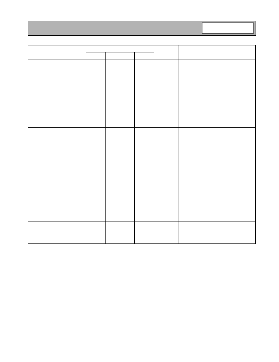
Product Description
Ordering Information
Typical Applications
Features
Functional Block Diagram
RF Micro Devices, Inc.
7628 Thorndike Road
Greensboro, NC 27409, USA
Tel (336) 664 1233
Fax (336) 664 0454
http://www.rfmd.com
Optimum Technology MatchingÆ Applied
Si BJT
GaAs MESFET
GaAs HBT
Si Bi-CMOS
SiGe HBT
Si CMOS
InGaP/HBT
GaN HEMT
SiGe Bi-CMOS
GND
GND
RF OUT
VCC2
PDET_OUT
VM
O
D
E
PA
_
O
N
VCC3
GND
GND
RF IN
VCC1
Bias
Pwr
Det
12
11
1
2
3
4
5
10
9
8
7
6
RF3300-2
3V 900MHz LINEAR AMPLIFIER MODULE
∑ 3V CDMA/AMPS Cellular Handsets
∑ 3V CDMA2000/1X Cellular Handsets
∑ Spread-Spectrum Systems
∑ Designed for Compatibility with Qualcomm
Chipsets
The RF3300-2 is a high-power, high-efficiency linear
amplifier module targeting 3V handheld systems. The
device is manufactured on an advanced Gallium Arsenide
Heterojunction Bipolar Transistor (HBT) process, and has
been designed for use as the final RF amplifier in dual-
mode 3V CDMA/AMPS handheld digital cellular equip-
ment, spread-spectrum systems, and other applications
in the 824MHz to 849MHz band. The RF3300-2 has a
digital control line for low power application to reduce the
current drain. The device is self-contained with 50
input
and output that is matched to obtain optimum power, effi-
ciency, and linearity characteristics. The RF3300-2 con-
tains a temperature compensating bias circuit to improve
performance over temperature.
∑ Single 3V Supply with Internal V
REF
∑ Integrated Power Detect Circuit
∑ 27dB Linear Gain
∑ 55mA Idle Current
∑ Temperature Compensating Bias Circuit
∑ Integrated PA Enable Switch
RF3300-2
3V 900MHz Linear Amplifier Module
RF3300-2 PCBA Fully Assembled Evaluation Board
0
Rev A6 030124
NOTES:
Nominal thickness, 1.55
mm.
Note orientation of Pin 1.
Dimensions in mm.
1
0.
12
5 T
Y
P
7.375 TYP
6.775
6.575 TYP
5.875 TYP
5.075 TYP
4.375 TYP
3.575 TYP
2.875 TYP
2.075 TYP
0.925 TYP
0.000
0.125 TYP
Bottom View
4.3
7
5
3.5
7
5
2.4
2
5
1.6
2
5
0.
00
0
0.
92
5 T
Y
P
1.
75
0
4.
25
0
5.
07
5 T
Y
P
5
.
87
5 T
Y
P
Package Style: Module (6mmx7.5mm)

2-540
RF3300-2
Rev A6 030124
Absolute Maximum Ratings
Parameter
Rating
Unit
Supply Voltage (RF off)
+8.0
V
DC
Supply Voltage
(P
OUT
31.5dBm)
+5.2
V
DC
Control Voltage (PA_ON)
+3.6
V
DC
Input RF Power
+10
dBm
Mode Voltage (V
MODE
)
+3.6
V
DC
Operating Case Temperature
-30 to +110
∞C
Storage Temperature
-30 to +150
∞C
Parameter
Specification
Unit
Condition
Min.
Typ.
Max.
High Power State
(V
MODE
Low)
Typical Performance at V
CC
=3.2V,
PA_ON=High, T
AMB
=25∞C,
Frequency=824MHz to 849MHz
(unless otherwise specified)
Frequency Range
824
849
MHz
Linear Gain
27
dB
See Gain versus Power chart.
Second Harmonic
-40
dBc
Third Harmonic
-40
dBc
Maximum Linear Output Power
(CDMA Modulation)
28
dBm
Total Linear Efficiency
33
%
V
CC
=3.2V, P
OUT
=28dBm
(room temperature)
Adjacent Channel Power
Rejection
-48
-46
dBc
ACPR@885kHz, P
OUT
=Max P
OUT
-60
-59
dBc
ACPR@1980kHz, P
OUT
=Max P
OUT
Input VSWR
1.8:1
Output VSWR
10:1
No damage.
6:1
No oscillations. >-70dBc
Noise Power
-135
dBm/Hz
At 45MHz offset.
Low Power State
(V
MODE
High)
Typical Performance at V
CC
=3.2V,
PA_ON=High, T
AMB
=25∞C,
Frequency=824MHz to 849MHz
(unless otherwise specified)
Frequency Range
824
849
MHz
Linear Gain
24.5
dB
Second Harmonic
-40
dBc
Third Harmonic
-35
dBc
Maximum Linear Output Power
(CDMA Modulation)
16
dBm
Adjacent Channel Power
Rejection
-46.5
-44.0
dBc
ACPR@885kHz, P
OUT
=Max P
OUT.
See ACPR versus Power chart.
-62
-59
dBc
ACPR@1980kHz, P
OUT
=Max P
OUT
Input VSWR
1.8:1
Output VSWR
10:1
No damage.
6:1
No oscillations. >-70dBc
Caution! ESD sensitive device.
RF Micro Devices believes the furnished information is correct and accurate
at the time of this printing. However, RF Micro Devices reserves the right to
make changes to its products without notice. RF Micro Devices does not
assume responsibility for the use of the described product(s).
2-541
RF3300-2
Rev A6 030124
Parameter
Specification
Unit
Condition
Min.
Typ.
Max.
FM Mode
Typical Performance at V
CC
=3.2V,
PA_ON=High, T
AMB
=25∞C,
Frequency=824MHz to 849MHz
(unless otherwise specified)
Frequency Range
824
849
MHz
Gain
27
dB
Second Harmonic
-40
dBc
Third Harmonic
-40
dBc
Max CW Output Power
31.5
dBm
Total Efficiency (AMPS mode)
48
%
V
CC
=3.2V,
P
OUT
=31.5dBm (room temperature)
Input VSWR
1.8:1
Output VSWR
10:1
No damage.
6:1
No oscillations. >-70dBc
DC Supply
Supply Voltage Range
3.2
3.7
4.2
V
Quiescent Current
100
120
mA
V
MODE
=Low
55
70
mA
V
MODE
=High
PA_ON Current
0.1
µ
A
V
MODE
=High
V
MODE
Current
0.1
µ
A
Turn On/Off Time
<40
µ
s
PA_ON switch from Low to High,
I
CC
to within 90% of the final value,
P
OUT
within 1dB of the final value
Total Current (Power Down)
35
60
µ
A
PA_ON=Low, V
MODE
=Low
PA_ON "Low" Voltage Range
0
0.5
V
PA_ON "High" Voltage Range
1.7
2.7
3.6
V
Must not exceed V
CC
.
V
MODE
"Low" Voltage Range
0
0.5
V
V
MODE
"High" Voltage Range
1.7
2.7
3.6
V
Must not exceed V
CC
.
Gain Settle Time
6
µ
s
PA_ON switched from low to high,
P
OUT
within 1dB of the final value.
6
µ
s
PA_ON switched from high to low,
P
OUT
within 1dB of the final value.
Internal Power Detector
PDET Output Voltage
1.8
V
P
OUT
=28dBm, V
MODE
=Low, CDMA Mode
1
V
P
OUT
=16dBm, V
MODE
=High, CDMA Mode
2.1
V
P
OUT
=31.5dBm, V
MODE
=Low, FM Mode
2-542
RF3300-2
Rev A6 030124
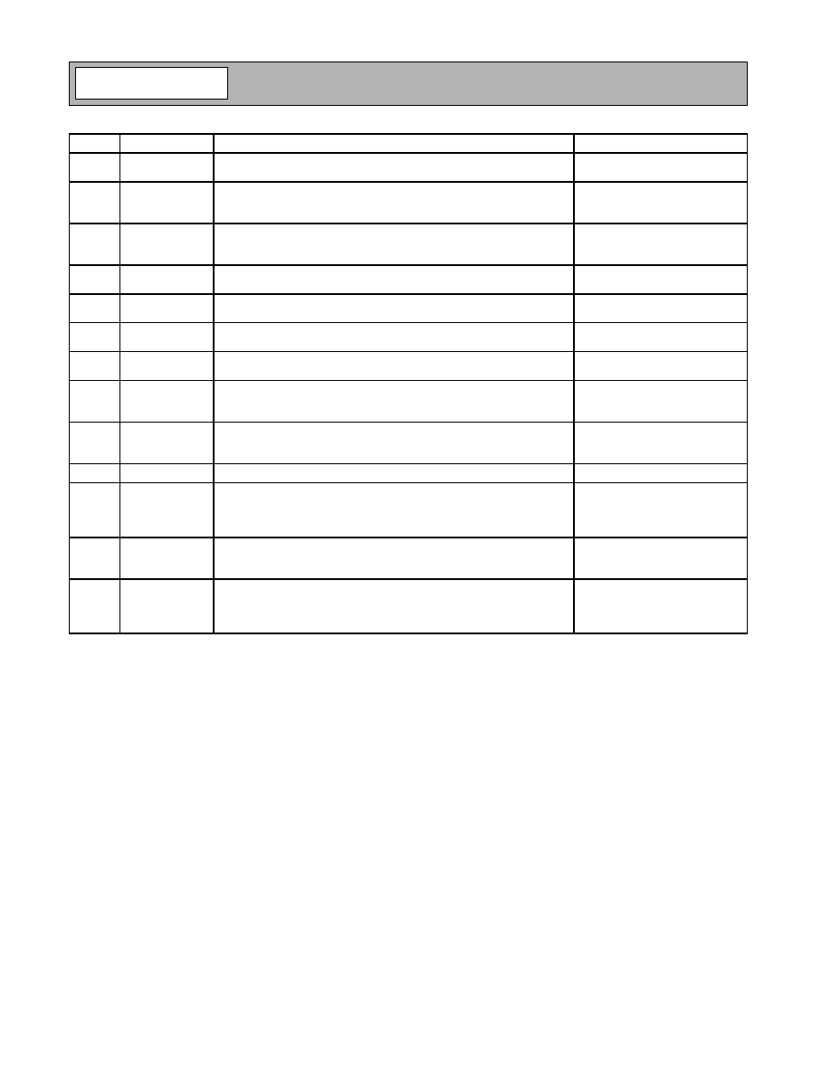
Pin
Function
Description
Interface Schematic
1
VCC3
Bias circuit and HDET power supply. A low frequency decoupling
capacitor (2.2
µ
F) is required. Type: P
2
GND
Ground connection. Connect to the GND_SLUG pin. For best perfor-
mance, keep traces physically short and connect immediately to
ground plane. Type: P
3
GND
Ground connection. Connect to the GND_SLUG pin. For best perfor-
mance, keep traces physically short and connect immediately to
ground plane. Type: P
4
RF IN
RF input internally matched to 50
. This input is internally AC-coupled.
Type: A, I
5
VCC1
First stage power supply. A low frequency decoupling capacitor (2.2
µ
F)
is required. Type: P
6
VCC2
Output stage power supply. A low frequency decoupling capacitor
(2.2
µ
F) is required. Type: P
7
RF OUT
RF output internally matched to 50
. This input is internally AC-cou-
pled. Type: A, O
8
GND
Ground connection. Connect to the GND_SLUG pin. For best perfor-
mance, keep traces physically short and connect immediately to
ground plane. Type: P
9
GND
Ground connection. Connect to the GND_SLUG pin. For best perfor-
mance, keep traces physically short and connect immediately to
ground plane. Type: P
10
PDET_OUT
Power detector output. Type: A, O
11
VMODE
Gain step control. When this pin is High, the module is in low power
mode, and the amplifier's current is reduced. When this pin is Low, the
module is in high power mode. Voltage should not be applied to this pin
before VCC3 is applied. Type: D, I
12
PA_ON
Device enable control. When this pin is High, the device is on. When
this pin is Low, the device is off. Voltage should not be applied to this
pin before VCC3 is applied. Type: D, I
13
GND_SLUG
Ground connection. The backside of the package should be soldered to
a top side ground pad which is connected to the ground plane with mul-
tiple vias. The pad should have a short thermal path to the ground
plane.
Note: Where Type code is:
I=Input; O=Output; A=Analog; D=Digital; P=Power

2-543
RF3300-2
Rev A6 030124
Evaluation Board Schematic
(Download Bill of Materials from www.rfmd.com.)
PA_ON
VMODE
PDET_OUT
VCC3
C3
2.2
µ
F
50
µ
strip
J1
RF IN
VCC1
C1
2.2
µ
F
VCC2
C2
2.2
µ
F
50
µ
strip
J2
RF OUT
Bias
Pwr
Det
12
11
1
2
3
4
5
10
9
8
7
6
R2
100 k
R3
100 k
R1
1 k
C4
10 nF
NOTE:
Resistors R2 and R3 are provided on the evaluation board to protect against power sequencing
issues. (Refer to pin descriptions 11 and 12.) These resistors are not needed when the VCC3 is
connected to the handset battery.

2-544
RF3300-2
Rev A6 030124
Low Power Idle Current versus V
CC
(V
CC
= 3.2V)
40.0
45.0
50.0
55.0
60.0
65.0
70.0
3.2
3.7
4.2
V
CC
(V)
Idle Current (mA)
Low Idle Icq (25C)
Low Idle Icq (-30C)
Low Idle Icq (100C)
High Power Adjacent Channel Power Versus Output Power
(V
CC
= 3.2V)
-70.0
-68.0
-66.0
-64.0
-62.0
-60.0
-58.0
-56.0
-54.0
-52.0
-50.0
-48.0
16.0
18.0
20.0
22.0
24.0
26.0
28.0
P
OUT
(dBm)
High Power ACPR (dBc)
ACP (25C, 3.2V, 824MHz)
ACP (25C, 3.2V, 836.5MHz)
ACP (25C, 3.2V, 849MHz)
ACP (-30C, 3.2V, 824MHz)
ACP (-30C, 3.2V, 836.5MHz)
ACP (-30C, 3.2V, 849MHz)
ACP (100C, 3.2V, 824MHz)
ACP (100C, 3.2V, 836.5MHz)
ACP (100C, 3.2V, 849MHz)
High Power Alternate Channel Power versus
Output Power
(V
CC
= 3.2V)
-68.0
-66.0
-64.0
-62.0
-60.0
16.0
18.0
20.0
22.0
24.0
26.0
28.0
P
OUT
(dBm)
High Power Alt (dBc)
ALT (25C, 3.2V, 824MHz)
ALT (25C, 3.2V, 836.5MHz)
ALT (25C, 3.2V, 849MHz)
ALT (-30C, 3.2V, 824MHz)
ALT (-30C, 3.2V, 836.5MHz)
ALT (-30C, 3.2V, 849MHz)
ALT (100C, 3.2V, 824MHz)
ALT (100C, 3.2V, 836.5MHz)
ALT (100C, 3.2V, 849MHz)
High Power CDMA Gain versus Output Power
(V
CC
=3.2V)
21.0
22.0
23.0
24.0
25.0
26.0
27.0
28.0
16.0
18.0
20.0
22.0
24.0
26.0
28.0
P
OUT
(dBm)
High Power Gain (dB)
Gain (25C, 3.2V, 824MHz)
Gain (25C, 3.2V, 836.5MHz)
Gain (25C, 3.2V, 849MHz)
Gain (-30C, 3.2V, 824MHz)
Gain (-30C, 3.2V, 836.5MHz)
Gain (-30C, 3.2V, 849MHz)
Gain (100C, 3.2V, 824MHz)
Gain (100C, 3.2V, 836.5MHz)
Gain (100C, 3.2V, 849MHz)
Low Power Adjacent Channel Power versus
Output Power
(V
CC
=3.2)
-58.0
-56.0
-54.0
-52.0
-50.0
-48.0
-46.0
-44.0
0.0
2.0
4.0
6.0
8.0
10.0
12.0
14.0
16.0
P
OUT
(dBm)
Adjacent Channel Power (dBc)
ACP (25C, 3.2V, 824MHz)
ACP (25C, 3.2V, 836.5MHz)
ACP (25C, 3.2V, 849MHz)
ACP (-30C, 3.2V, 824MHz)
ACP (-30C, 3.2V, 836.5MHz)
ACP (-30C, 3.2V, 849MHz)
ACP (100C, 3.2V, 824MHz)
ACP (100C, 3.2V, 836.5MHz)
ACP (100C, 3.2V, 849MHz)
Low Power Alternate Channel Power versus
Output Power
(V
CC
=3.2V)
-67.0
-66.5
-66.0
-65.5
-65.0
-64.5
-64.0
-63.5
-63.0
-62.5
-62.0
0.0
2.0
4.0
6.0
8.0
10.0
12.0
14.0
16.0
P
OUT
(dBm)
Alternate Channel Power (dBc)
ALT (25C, 3.2V, 824MHz)
ALT (25C, 3.2V, 836.5MHz)
ALT (25C, 3.2V, 849MHz)
ALT (-30C, 3.2V, 824MHz)
ALT (-30C, 3.2V, 836.5MHz)
ALT (-30C, 3.2V, 849MHz)
ALT (100C, 3.2V, 824MHz)
ALT (100C, 3.2V, 836.5MHz)
ALT (100C, 3.2V, 849MHz)

2-545
RF3300-2
Rev A6 030124
Low Power Gain versus Output Power
(V
CC
= 3.2V)
12.0
14.0
16.0
18.0
20.0
22.0
24.0
26.0
28.0
0.0
2.0
4.0
6.0
8.0
10.0
12.0
14.0
16.0
P
OUT
(dBm)
Low Power Gain (dB)
Gain (25C, 3.2V, 824MHz)
Gain (25C, 3.2V, 836.5MHz)
Gain (25C, 3.2V, 849MHz)
Gain (-30C, 3.2V, 824MHz)
Gain (-30C, 3.2V, 836.5MHz)
Gain (-30C, 3.2V, 849MHz)
Gain (100C, 3.2V, 824MHz)
Gain (100C, 3.2V, 836.5MHz)
Gain (100C, 3.2V, 849MHz)

2-546
RF3300-2
Rev A6 030124