3-27
3
LI
N
E
A
R
C
A
TV
A
M
P
L
IF
IE
R
S
Preliminary
Product Description
Ordering Information
Typical Applications
Features
Functional Block Diagram
RF Micro Devices, Inc.
7625 Thorndike Road
Greensboro, NC 27409, USA
Tel (336) 664 1233
Fax (336) 664 0454
http://www.rfmd.com
Optimum Technology MatchingÆ Applied
Si BJT
GaAs MESFET
GaAs HBT
Si Bi-CMOS
¸
SiGe HBT
Si CMOS
1
2
3
4
5
6
7
8
16
15
14
13
12
11
10
9
SHDNB
TX EN
NC
VIN
VINB
VCC
VCC
RAMP
GND
NC
NC
VOUT
VOUTB
SDA
CS
SCLK
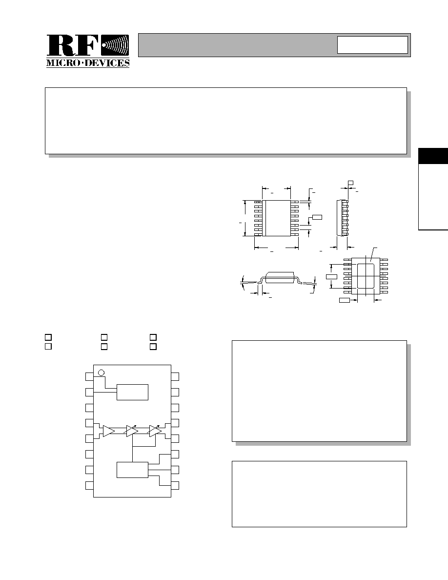
Power
Control
Gain Control
and Serial Bus
RF3320
CABLE REVERSE PATH
PROGRAMMABLE GAIN AMPLIFIER
∑ Euro-DOCSIS/DOCSIS Cable Modems
∑ CATV Set-Top Boxes
∑ Telephony Over Cable
∑ Home Networks
∑ Automotive/Mobile Multimedia
∑ Coaxial and Twisted Pair Line Driver
The RF3320 is a variable gain amplifier for use in CATV
reverse path (upstream) applications. It is DOCSIS-com-
pliant for use in cable modems. The gain control covers a
58dB range and is serially programmable via three-wire
digital bus for compatibility with standard baseband
chipsets. Amplifier shutdown and transmit disable modes
are software- and hardware-controlled. The device is
placed into software-shutdown mode via the serial control
bus. The device operates over the frequency band of
5 MHz to 65MHz for use in current U.S. and European
systems. The amplifier delivers up to 60dBmV at the out-
put of the balun. Gain is controllable in accurate 1 dB
steps. The device is provided in a thermally enhanced,
exposed die flag package.
∑ Single 5V Supply
∑ Differential Input and Output
∑ -30dB to +28dB Voltage Gain Range
∑ 5MHz to 65MHz Operation
∑ Sophisticated Power Management
∑ DOCSIS 1.1 RF Compliant
RF3320
Cable Reverse Path Programmable Gain Amplifier
RF3320 PCBA
Fully Assembled Evaluation Board
3
Rev A10 010514
NOTES:
1. Shaded lead is pin 1.
2. Lead coplanarity - 0.10 with
respect to datum "A".
3. Lead standoff is specified from
the lowest point on the package
underside.
8∞ MAX
0∞ MIN
0.60
+ 0.15
0.24
0.20
3.90
+ 0.10
0.25
+ 0.05
0.65
6.00
+ 0.20
4.90
+ 0.20
EXPOSED DIE
FLAG
3.302
2.286
1.40
+ 0.10
0.05
+ 0.05
Note 3
-A-
Package Style: SSOP-16 EDF Slug

Preliminary
3-28
RF3320
Rev A10 010514
3
LI
N
E
A
R
C
A
TV
A
M
P
L
IF
IE
R
S
Absolute Maximum Ratings
Parameter
Rating
Unit
Supply Voltage
-0.5 to +6.0
V
DC
Input RF Level
12
dBm
Operating Ambient Temperature
-40 to +85
∞C
Storage Temperature
-40 to +150
∞C
Humidity
80
%
Maximum Power Dissipation
0.5
W
Maximum T
J
150
∞C
Parameter
Specification
Unit
Condition
Min.
Typ.
Max.
Overall
V
CC
= 4.75V to 5.25V, TXEN= SHDNB =1,
V
IN
=30dBmV (rms) differential, output
impedance= 75
through a 2:1 transformer.
Typical performance is at T
A
= +25∞C,
V
CC
=5V.
DC Specifications
Supply Voltage
4.75
5.0
5.25
V
Supply Current
Maximum Gain
130
160
mA
Gain Control Word= 58
Low Gain
65
105
mA
Gain Control Word<35
Transmit Disable
25
35
mA
TXEN= 0
Software-Shutdown
3
5
mA
Bit 7 of gain control word FALSE
Sleep
0.05
mA
SHDNB= 0
Logic High Voltage
2
V
Logic Low Voltage
0.8
V
Logic Leakage Current
-1
1
µ
A
AC Specifications
Voltage Gain
Maximum
27
28
dB
5MHz to 42MHz; Gain Control Word= 58
26
dB
42MHz to 65MHz; Gain Control Word= 58
Minimum
-30
-29
dB
5MHz to 42MHz; Gain Control Word= 0
-28
dB
42MHz to 65MHz; Gain Control Word=0
3dB Bandwidth
100
MHz
Intended operating range is 5MHz to
65MHz.
1dB Compression Point
66
dBmV
Maximum Input Level
34
dBmV(rms)
Modulated. To meet distortion specifications.
Maximum Output Level
60
dBmV(rms)
Modulated. Into 75
load at balun output, all
distortion tones < -50dBc.
ACPR
-59
-47
dBc
V
IN
=34dBmV (rms); QPSK modulation;
Symbol rate= 160ksps (2 bits per symbol);
20-bit PRBS (pseudo-random bit stream);
0.25 alpha root cosine filter
Output IM3
-58
-55
dBc
Tones at 40MHz and 40.2MHz,
V
OUT
= +54dBmV/tone, maximum gain, OIP3
is therefore +84dBmV, IIP3 is 58dBmV.
Output Third Harmonic
Distortion
F =20MHz, V
OUT
= 59dBmV
-60
-55
dBc
Maximum Gain, CW
F =65MHz, V
OUT
= 59dBmV
-55
-50
dBc
Maximum Gain, CW
Output Second Harmonic
Distortion
F =20MHz, V
OUT
=59dBmV
-70
-60
dBc
Maximum Gain
F =65MHz, V
OUT
=59dBmV
-70
-60
dBc
Maximum Gain
Caution! ESD sensitive device.
RF Micro Devices believes the furnished information is correct and accurate
at the time of this printing. However, RF Micro Devices reserves the right to
make changes to its products without notice. RF Micro Devices does not
assume responsibility for the use of the described product(s).

Preliminary
3-29
RF3320
Rev A10 010514
3
LI
N
E
A
R
C
A
TV
A
M
P
L
IF
IE
R
S
Note 1: The enable time is determined by the value of the capacitor on pin 8 (RAMP). A higher capacitor value will
increase the enable time, but will reduce the transient voltage.
Parameter
Specification
Unit
Condition
Min.
Typ.
Max.
AC Specifications, cont'd
Output Step Size
0.8
1.0
1.1
dB
Isolation in Transmit Disable
Mode
-80
-95
dBc
Maximum Gain, 20MHz
Output Noise
Maximum Gain
-37
-30
dBmV/
160kHz
-96dBc for a 59dBmV carrier in a 160kHz
bandwidth.
Minimum Gain
-55
-50
dBmV/
160kHz
-64dBc for an 8dBmV carrier in a 160kHz
bandwidth.
Transmit Disabled
-75
-70
dBmV/
160kHz
TXEN =0
TX EN Enable Time
0.5
1.0
µ
S
Time for gain to reach 99% of final value.
See Note 1.
TX EN Transient Duration
2.4
3.0
µ
S
See Note 1.
Output Switching Transients
5
10
mV
P-P
Maximum Gain
3
5
mV
P-P
Minimum Gain
Output Impedance
255
300
345
Chip output impedance is nominally 300
.
Differential to single-ended output conver-
sion to 75
is performed in a balun with a
2:1 turns ratio, corresponding to a 4:1 imped-
ance ratio.
Input Impedance
75
Differential
Thermal
Theta
JC
28
∞C/W
Preliminary
3-30
RF3320
Rev A10 010514
3
LI
N
E
A
R
C
A
TV
A
M
P
L
IF
IE
R
S
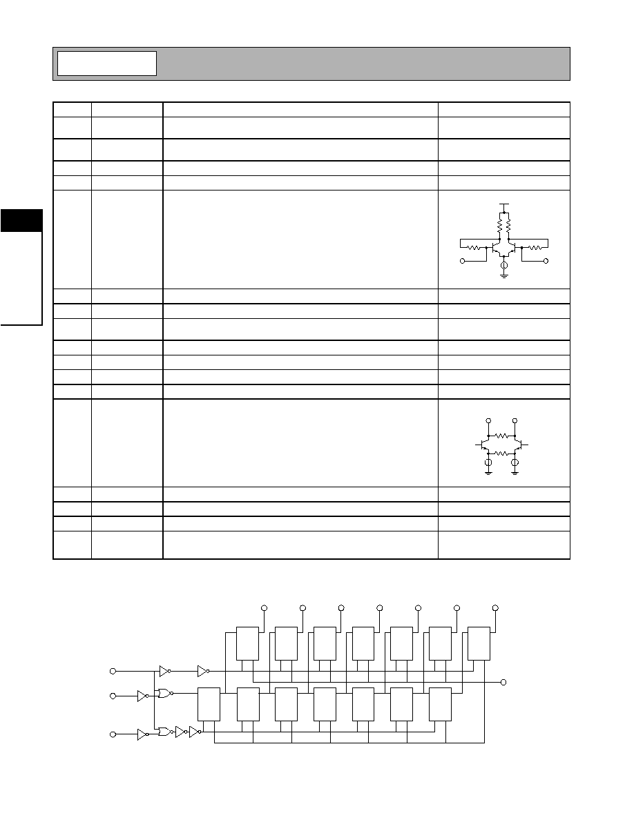
Serial Bus Block Diagram
Pin
Function
Description
Interface Schematic
1
SHDNB
Chip shutdown pin. Forcing a logic low causes all circuits to switch off
and gain settings to be lost.
2
TX EN
Signal path enable pin. Logic high turns on signal path. Logic low turns
off signal path, but leaves serial bus active.
3
NC
Not connected. This pin should be grounded.
4
VIN
Input pin. This should be externally AC-coupled to signal source.
See pin 5.
5
VINB
Complementary input pin. This should be externally coupled to signal
source. For single-ended use, this pin should be AC-coupled to ground.
6
VCC
This pin is connected to the supply voltage.
7
VCC
Same as pin 6.
8
RAMP
An external capacitor between this pin and ground controls turn-on
time.
9
SCLK
Serial bus clock input.
10
CS
Serial bus enable.
11
SDA
Serial bus data input.
12
VOUTB
Open collector output. Connect to VCC via balun primary.
See pin 13.
13
VOUT
Open collector output. Connect to VCC via balun primary.
14
NC
Same as pin 3.
15
NC
Same as pin 3.
16
GND
Connect to ground.
PKG
BASE
GND
Die is mounted on a heat sink slug that should be connected to ground.
Device grounds are internally bonded to the slug.
550
550
V
CC
500
500
V
INB
V
IN
300
V
OUT
V
OUTB
RE
D
CK
Q
CLR
D
CK
Q
CLR
D
CK
Q
CLR
D
CK
Q
CLR
D
CK
Q
CLR
D
CK
Q
CLR
D
CK
Q
CLR
D
CK
Q
CLR
D
CK
Q
CLR
D
CK
Q
CLR
D
CK
Q
CLR
D
CK
Q
CLR
D
CK
Q
CLR
D
CK
Q
CLR
D0
D1
D2
D3
D4
D5
D6
POR
CS
SDA
SCLK

Preliminary
3-31
RF3320
Rev A10 010514
3
LI
N
E
A
R
C
A
TV
A
M
P
L
IF
IE
R
S
Table 1. Serial Interface Control Word Format
Serial Bus Timing Diagram
Table 2. Timing Data
Table 3. Programming State
Bit
Mnemonic
Description
MSB 6
D6
Sleep Mode (Software Shutdown)
5
D5
Gain Control, Bit MSB
4
D4
Gain Control, Bit 4
3
D3
Gain Control, Bit 3
2
D2
Gain Control, Bit 2
1
D1
Gain Control, Bit 1
LSB 0
D0
Gain Control, Bit LSB
Parameter
Symbol
Min
Typ
Max
Units
SCLK Pulsewidth
T
WH
50
ns
SCLK Period
T
C
100
ns
Setup Time, SDA versus S CLK
T
DS
10
ns
Setup Time, CS versus S CLK
T
ES
10
ns
Hold Time, SDA versus S CLK
T
DH
20
ns
Hold Time, CS versus S CLK
T
EH
20
ns
SCLK Pulsewidth, High
T
DATAH
50
ns
SCLK Pulsewidth, Low
T
DATAL
50
ns
TX
SHDND
MSB6
Enter Sleep Mode
X
H
L
H= High Voltage Logic
Exit Sleep Mode
X
H
H*
L=Low Voltage Logic
Enter Shutdown
X
L
X
X =Don't Care
Exit Shutdown
X
H
H*
*Gain Control Data Must be Re-Sent
TX Enable
H
X
X
TX Disable
L
X
X
D0
D1
D2
D3
D4
D5
D6
T
ES
T
DS
T
DH
T
EH
T
WH
T
C
T
DATAH
,T
DATAL
CS
SCLK
SDA
(Data)

Preliminary
3-32
RF3320
Rev A10 010514
3
LI
N
E
A
R
C
A
TV
A
M
P
L
IF
IE
R
S
Typical Application Schematic
10 nF
10 nF
VIN
VINB
SDA
CS
SCLK
SHDNB
4:1
100 pF
VOUT
V
CC1
V
CC2
1
2
3
4
5
6
7
8
16
15
14
13
12
11
10
9
Power
Control
Gain Control
and Serial Bus
PACKAGE BASE
220 pF
TXEN

Preliminary
3-33
RF3320
Rev A10 010514
3
LI
N
E
A
R
C
A
TV
A
M
P
L
IF
IE
R
S
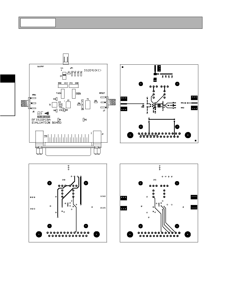
Evaluation Board Schematic
PCB Layout Considerations
The RF3320 Evaluation board can be used as a guide for the layout in your application. Care should be taken in laying
out the RF3320 in other applications. The RF3320 will have similar results if the following guidelines are taken into con-
sideration:
∑
Make sure underside of package is soldered to a good ground on the PCB.
∑
Keep input and output traces as short as possible.
∑
Ensure a good ground plane by using multiple vias to the ground plane.
∑
Use a low noise power supply along with decoupling capacitors.
C3
1 nF
C4
1 nF
T2
4:1
C9
100 pF
C8
15 pF
C7
15 pF
R5
24
J7
RF OUT
VCC2
T1
1:1
R4
75
R3
75
J6
RF IN
VCC1
C5
0.1
µ
F
SDA
CS
SCLK
1
2
3
4
5
6
7
8
9
10
11
12
13
14
15
16
17
18
19
20
21
22
23
24
25
R1
100 k
R2
100 k
VCC
NC
CS
SDA
SCLK
SHDNB
TXEN
NC
NC
GND
GND
GND
GND
GND
GND
GND
GND
VCC
VCC
NC
NC
NC
NC
NC
NC
CS
SDA
J5-1
J3-1
SCLK
J1
J3
1
2
3
J1-6
TXEN
J2
1
2
3
VCC
GND
J5
1
2
3
J1-5
SHDNB
J4
1
2
3
VCC
GND
JP1
1
2
VCC
GND
+
C2
1 nF
L1 (Ferrite)
30
C1
10
µ
F
(10 V)
L3 (Ferrite)
30
L4 (Ferrite)
30
L2 (Ferrite)
30
VCC
VCC1
VCC2
1
2
3
4
5
6
7
8
16
15
14
13
12
11
10
9
Power
Control
Gain Control
and Serial Bus
PACKAGE BASE
C6
220 pF
Notes:
1. 4-layer board.
2. Underside of package must solder to ground.
3. Place C5 and C6 as close to pin as possible.
4. C1 is tantalum, size code Y.
5. All other components are 0603 size.
6. Replace R5 with 0
resistor if 75
connector is used.
3320400B
Preliminary
3-34
RF3320
Rev A10 010514
3
LI
N
E
A
R
C
A
TV
A
M
P
L
IF
IE
R
S
Evaluation Board Layout
Board Size 2.5" x 2.5"
Board Thickness 0.058", Board Material FR-4
Preliminary
3-35
RF3320
Rev A10 010514
3
LI
N
E
A
R
C
A
TV
A
M
P
L
IF
IE
R
S
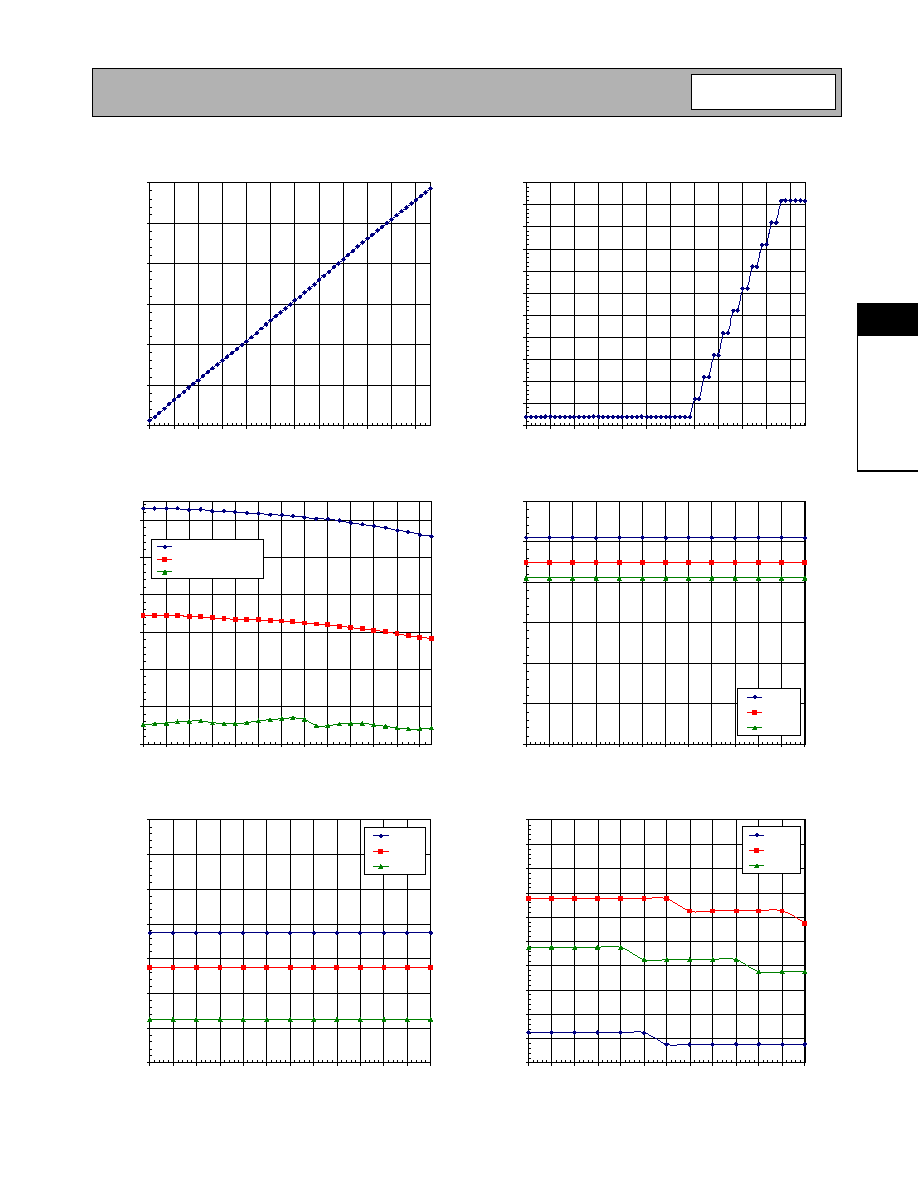
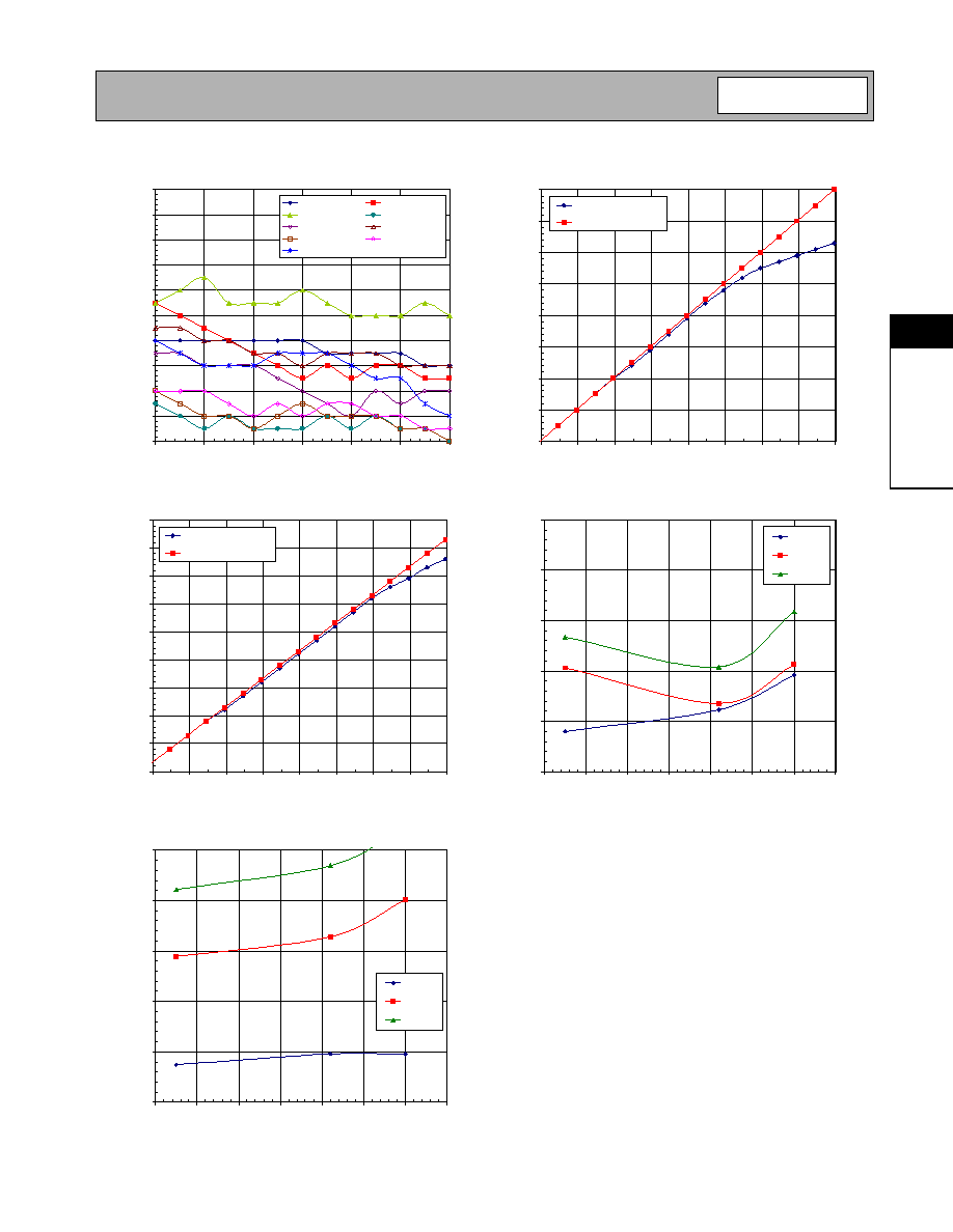
Gain versus Gain Control Word
at 5 MHz
-32.0
-22.0
-12.0
-2.0
8.0
18.0
28.0
0.0
5.0
10.0
15.0
20.0
25.0
30.0
35.0
40.0
45.0
50.0
55.0
Gain Control Word
Gain
(dB)
Current versus Gain Control Word
90.0
95.0
100.0
105.0
110.0
115.0
120.0
125.0
130.0
135.0
140.0
145.0
0.0
5.0
10.0
15.0
20.0
25.0
30.0
35.0
40.0
45.0
50.0
55.0
Gain Control Word
Current
(mA)
Gain versus Frequency
-35
-25
-15
-5
5
15
25
5
25
45
65
85
105
125
145
165
185
205
225
245
Frequency (MHz)
Voltage
Gain
(dB)
Gain Control Word = 58
Gain Control Word = 29
Gain Control Word = 0
Gain versus Supply Voltage
(GCW = 58)
25.40
25.90
26.40
26.90
27.40
27.90
28.40
4.70 4.75 4.80
4.85
4.90 4.95 5.00 5.05 5.10
5.15
5.20 5.25 5.30
Voltage (V)
Gain
(dB)
5 MHz
42 MHz
65 MHz
Gain versus Supply Voltage
(GCW = 0)
-30.00
-29.80
-29.60
-29.40
-29.20
-29.00
-28.80
-28.60
-28.40
-28.20
-28.00
4.70 4.75 4.80
4.85 4.90
4.95 5.00 5.05 5.10 5.15 5.20
5.25 5.30
Voltage (V)
Gain
(dB)
5 MHz
42 MHz
65 MHz
Gain versus Supply Voltage
(GCW = 29)
-1.40
-1.20
-1.00
-0.80
-0.60
-0.40
-0.20
0.00
4.70
4.75
4.80 4.85 4.90
4.95
5.00 5.05 5.10
5.15
5.20 5.25 5.30
Voltage (V)
Gain
(dB)
5 MHz
42 MHz
65 MHz

Preliminary
3-36
RF3320
Rev A10 010514
3
LI
N
E
A
R
C
A
TV
A
M
P
L
IF
IE
R
S
Gain versus Frequency
at Gain Control Word = 58
24.0
24.5
25.0
25.5
26.0
26.5
27.0
27.5
28.0
28.5
5
55
105
155
205
255
Frequency (MHz)
Voltage
Gain
(dB)
Temp = 85∞C
Temp = 0∞C
Temp = -40∞C
Gain versus Frequency
at Gain Control Word = 25
-8.0
-7.0
-6.0
-5.0
-4.0
-3.0
-2.0
-1.0
0.0
5
55
105
155
205
255
Frequency (MHz)
Voltage
Gain
(dB)
Temp = 85∞C
Temp = 0∞C
Temp = -40∞C
Gain versus Frequency
at Gain Control Word = 0
-31.5
-31.0
-30.5
-30.0
-29.5
-29.0
-28.5
-28.0
-27.5
-27.0
-26.5
-26.0
5
55
105
155
205
255
Frequency (MHz)
Voltage
Gain
(dB)
Temp = 85∞C
Temp = 0∞C
Temp = -40∞C
Gain versus Gain Control Word
-30.0
-20.0
-10.0
0.0
10.0
20.0
30.0
0
10
20
30
40
50
Gain Control Word
Voltage
Gain
(dB)
85∞C
0∞C
-40∞C
Gain versus Supply Voltage
at Gain Control Word = 58
27.0
27.2
27.4
27.6
27.8
28.0
28.2
4.7
4.8
4.9
5.0
5.1
5.2
5.3
Supply Voltage (V)
Voltage
Gain
(dB)
5 MHz at 85∞C
42 MHz at 85∞C
65 MHz at 85∞C
5 MHz at 0∞C
42 MHz at 0∞C
65 MHz at 0∞C
5 MHz at -40∞C
42 MHz at -40∞C
65 MHz at -40∞C
Gain versus Supply Voltage
at Gain Control Word = 29
-1.4
-1.2
-1.0
-0.8
-0.6
-0.4
-0.2
0.0
4.7
4.8
4.9
5.0
5.1
5.2
5.3
Supply Voltage (V)
Voltage
Gain
(dB)
5 MHz at 85∞C
42 MHz at 85∞C
65 MHz at 85∞C
5 MHz at 0∞C
42 MHz at 0∞C
65 MHz at 0∞C
5 MHz at -40∞C
42 MHz at -40∞C
65 MHz at -40∞C
Preliminary
3-37
RF3320
Rev A10 010514
3
LI
N
E
A
R
C
A
TV
A
M
P
L
IF
IE
R
S
-1 dB Compression Point
(GCW = 58)
60.0
61.0
62.0
63.0
64.0
65.0
66.0
67.0
68.0
33.8
34.8
35.8
36.8
37.8
38.8
39.8
40.8
41.8
Power In (dBmV)
Power
O
ut
(dBmV)
Gain Control Word = 58
Trend
-1 dB Compression Point
(GCW = 29)
31.0
32.0
33.0
34.0
35.0
36.0
37.0
38.0
39.0
40.0
33.8
34.8
35.8
36.8
37.8
38.8
39.8
40.8
41.8
Power In (dBmV)
Power
O
ut
(dBmV)
Gain Control Word = 29
Trend
Second Harmonic versus Frequency and Output Level
-75.0
-70.0
-65.0
-60.0
-55.0
-50.0
0.0
10.0
20.0
30.0
40.0
50.0
60.0
70.0
Frequency (MHz)
Second
Harmonic
(
dBc)
30dBmV
57dBmV
60dBmv
Third Harmonic versus Frequency and Output Level
-75.0
-70.0
-65.0
-60.0
-55.0
-50.0
0.0
10.0
20.0
30.0
40.0
50.0
60.0
70.0
Frequency (MHz)
Third
H
armonic
(
dBc)
30dBmV
57dBmV
60dBmV
Gain versus Supply Voltage
at Gain Control Word = 0
-30.0
-29.8
-29.6
-29.4
-29.2
-29.0
-28.8
-28.6
-28.4
-28.2
-28.0
4.7
4.8
4.9
5.0
5.1
5.2
5.3
Supply Voltage (V)
Voltage
Gain
(dB)
5 MHz at 85∞C
42 MHz at 85∞C
65 MHz at 85∞C
5 MHz at 0∞C
42 MHz at 0∞C
65 MHz at 0∞C
5 MHz at -40∞C
42 MHz at -40∞C
65 MHz at -40∞C

Preliminary
3-38
RF3320
Rev A10 010514
3
LI
N
E
A
R
C
A
TV
A
M
P
L
IF
IE
R
S
CH1
S
11 log MAG
10 dB/
REF 0 dB
START 1.000 000 MHz
STOP 100.000 000 MHz
Cor
PRm
1
2
3
1: -19.249 dB
4.960 000 MHz
2: -20.665 dB
42.085 MHz
3: -21.65 dB
64.855 MHz
S
11
Transmit Enable = 5V
CH1
S
22
log MAG
10 dB/
REF 0 dB
START 1.000 000
STOP 100.000 000 MHz
Cor
PRm
1
2
3
1: -25.52 dB
4.960 000
2: -25.226 dB
42.085 MHz
3: -22.568 dB
64.855 MHz
S
22
Transmit Enable = 5V
CH1
S
11
log MAG
10 dB/
START 1.000 000 MHz
STOP 100.000 000 MHz
Cor
PRm
1
2
3
1: -19.335 dB
4.960 000 MHz
2: -20.627 dB
42.085 MHz
3: -21.815 dB
64.855 MHz
S
11
Transmit Enable = 0V
CH1
S
22
log MAG
10 dB/
START 1.000 000 MHz
STOP 100.000 000 MHz
Cor
PRm
1
2
3
1: -25.612 dB
4.960 000 MHz
2: -25.871 dB
42.085 MHz
3: -22.989 dB
64.855 MHz
S
22
Transmit Enable = 0V
Preliminary
3-39
RF3320
Rev A10 010514
3
LI
N
E
A
R
C
A
TV
A
M
P
L
IF
IE
R
S
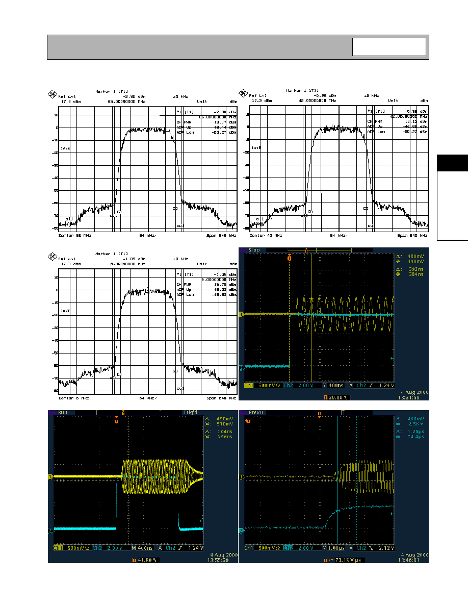
Power Up Settling Time Coming Out Of Shutdown Condition
Power Up Settling Time Coming Out Of Shutdown Condition (Entire Pulse)
Power Up Settling Time Coming Out Of Sleep Condition
ACPR at 65MHz
ACPR at 42MHz
ACPR at 5MHz

Preliminary
3-40
RF3320
Rev A10 010514
3
LI
N
E
A
R
C
A
TV
A
M
P
L
IF
IE
R
S
Evaluation Kit
General Description
The RF3320 PCBA is a fully assembled evaluation
board of the RF3320 reverse path high output power
programmable gain amplifier, useful for providing a
demonstration of the RF3320's functionality. The
RF3320 PCBA is a digitally controlled variable gain
amplifier capable of driving a 75
source. The RF3320
is designed to send cable modem data with QPSK or
QAM modulated format at frequencies between 5MHz
and 65MHz. The gain is controlled by an 7-bit serial
data word which adjusts the output gain from -30dB to
+28 dB.
The kit includes a fully functional evaluation board
along with a serial data cable and software. The cable
connects directly to the parallel port of a standard PC.
The software is used to control the serially programma-
ble gain through a simple, easy to understand user
interface.
Input and output to the evaluation board is provided
through 50
SMA connectors. The input and output of
the evaluation board is matched to 50
and connected
through a balun for single-ended operation. This allows
easy connection to test equipment, but the evaluation
board can easily be converted to a 75
input and out-
put, or for differential input and output. The output cir-
cuit is matched using a 24
series resistor which is
used to bring the load impedance up to 75
when
using standard 50
test equipment. This will introduce
a loss which must be accounted for in all measure-
ments (see measurement section and evaluation board
schematic for more detail).
PCBA Details
Input Circuit
The input to the RF3320 is differential and the imped-
ance is 75
; However, for ease of testing, the evalua-
tion board has been changed to single-ended and the
impedance has been matched to 50
. If a 75
input is
required, simply replace the 50
SMA connector with
a 75
F-style connector and remove R3 and R4.
Output Circuit
The output of the RF3320 is differential and the imped-
ance is 300
. In normal applications this is converted
into a single-ended 75
output using a 2:1 (voltage
ratio) transformer with a center-tap on the secondary
which supplies power to the output stage. The evalua-
tion board is configured for use with 50
test equip-
ment. This has been achieved with a 24
resistor in
series with the output to increase the load seen by the
device to 75
. This introduces a voltage loss of 3.5 dB
which must be accounted for in all measurements.
Some spectrum analyzers have a setting to account for
this method of 75
testing (e.g., on a Rhode &
Schwartz spectrum analyzer the input can be set to
'"75
RAZ" and the loss is accounted for automati-
cally). A more accurate way of making this measure-
ment is to use a 75
spectrum analyzer, or use a
matching transformer or minimum loss pad. This
ensures that the source impedance seen by the equip-
ment is also 75
. If a 75
output is required, simply
replace the 50
SMA connector (J7) with a 75
F-
style connector and replace R5 with a 0
jumper. The
evaluation board is tested with a Coilcraft balun; how-
ever, additional baluns may be used as long as care is
taken in modifying the decoupling capacitors around
the balun. These capacitors can greatly affect the har-
monic suppression. Other baluns may be used but
should be tested for second and third order harmonic
suppression.
Transmit Enable
The transmit enable can be set to "continuous on" by
placing the TXEN jumper in the up position (up position
when viewing the top of the evaluation board with the
25 pin connector closest to the viewer) and placing the
associated GND/V
CC
jumper in the "V
CC
" position. The
transmit enable can be set to "continuous off" by plac-
ing the GND/V
CC
jumper in the "GND" position. If a
computer controlled signal is used (J1), place the
TXEN jumper in the down position.
Software Controlled
C
TX EN
GND
VCC
Continuous OFF
B
GND
VCC
TX EN
Continuous ON
A
GND
VCC
TX EN
Figure 1. TX Enable Configuration

Preliminary
3-41
RF3320
Rev A10 010514
3
LI
N
E
A
R
C
A
TV
A
M
P
L
IF
IE
R
S
Shutdown Enable
Shutdown enable can be set to be "continuous on"
(chip enabled) by placing the SHDN jumper in the up
position and placing the associated GND/V
CC
jumper
in the "V
CC
" position. Shutdown enable can be set to
"continuous off" (chip disabled) by placing the associ-
ated GND/V
CC
jumper in the "GND" position. If a com-
puter controlled signal is used (J1), place the SHDN
jumper in the down position.
V
CC
Settings
V
CC1
should be set to 5.0V
DC
.
Evaluation Board Setup
Equipment Needed
∑
Signal Generator
∑
Spectrum Analyzer
∑
Power Supply (5.0 V@300 mA)
∑
RF3320 PCBA
∑
Serial Cable (included with kit)
∑
Standard PC
∑
Three-Wire Bus Software
Optional Equipment
∑
Variable Low-Pass or Band-Pass Filters
∑
Power Meter
∑
Second Signal Generator with Modulation for ACPR
and IP2, IP3 Testing
∑
Arbitrary Wave Generator
∑
Two-Channel Oscilloscope
Software Setup
To install the software, you need a computer with the
following.
∑
133MHz Pentium processor
∑
16MB RAM
∑
Hard Drive with 5MB free space
∑
Free 25-pin LPT port
∑
VGA Monitor
The software may be downloaded from www.rfmd.com
by following these steps.
Select the "Product Support" tab;
Select "Evaluation Board Information";
Select "RF3320".
Unzip the file using WinZip 7.0 or higher (http://
www.winzip.com). Unzip to a temporary directory and
run RF3320.exe.
The 7-bit Gain Control Word (GCW) in the data latch
determines the gain setting in the RF3320. The gain
control data (SDA) load sequence is initiated by a fall-
ing edge on CS. The SDA is serially loaded (LSB first)
into the 7-bit shift register at each rising edge of the
clock. While CS is low, the data latch holds the previ-
ous data word allowing the gain level to remain
unchanged. After seven clock cycles the new data
word is fully loaded and CS is switched high. This
enables the data latch and the loaded register data is
passed to the gain control block with the updated gain
value. Also at this CS transition, the internal clock is
disabled, thus inhibiting new serial input data.
Software and Cable
Figure 3 shows the cable configuration. Connect the
cable into the LPT1 port of the computer running the
software. Connect the other end of the cable to the 25-
pin connector of the evaluation board. Executing the
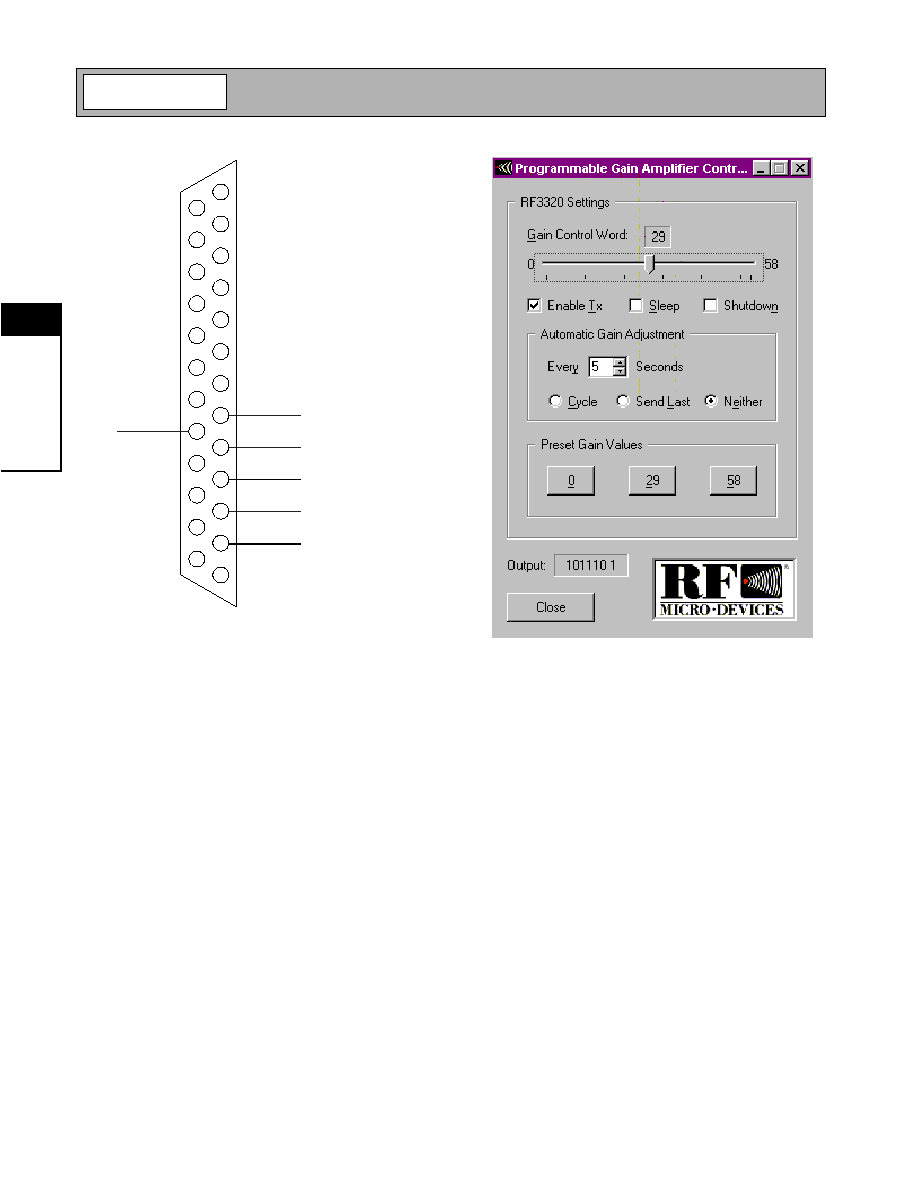
software (RF3320.exe) will produce the screen shown
in Figure 4. The user may set the gain of the evaluation
board by sliding the gain control switch to the desired
gain setting. Pressing the Preset Gain Value buttons
automatically sets the gain of the unit to the value
shown on the button. The Automatic Gain Adjustment
when set to "Cycle" will automatically cycle through all
of the gain steps (0-58) in seconds (at the rate set by
the user). The user may place the unit in sleep, shut-
down and transmit enable/disable modes by checking
the corresponding box. The bit pattern being sent to
the PCBA is shown at the bottom of the screen. See
README_3320.txt file for proper pin/signal mapping
for the 25 pin interface.
Software Controlled
C
GND
VCC
SHDN
Continuous ON
B
SHDN
GND
VCC
Continuous OFF
A
GND
VCC
SHDN
Figure 2. SHDN Enable Configuration
Preliminary
3-42
RF3320
Rev A10 010514
3
LI
N
E
A
R
C
A
TV
A
M
P
L
IF
IE
R
S
Hardware Setup
Gain and Harmonic Distortion Test Setup
To test the gain of the RF3320 PCBA, connect a low-
pass or band-pass filter to the output of the signal gen-
erator. Use a filter just above the frequency you want to
test. The filter is used to attenuate any harmonics out-
put by the signal generator. Connect the signal genera-
tor to the power meter and measure the power.
Compare with modulation enabled and disabled to
make sure the meter was measuring average rather
than peak power. No more than 0.2 dB difference in
power should be observed. An offset on the signal gen-
erator may be needed to match the level shown on the
power meter. The signal generator should then be con-
nected directly to a spectrum analyzer. Make sure the
output of the signal generator is the same as the input
read by the spectrum analyzer. Adjust the offset of the
spectrum analyzer until the signal out is the same as
the signal in on the spectrum analyzer. Turn off the RF
and modulation. Check positioning of the jumpers on
the board. Refer to the PCBA section of this applica-
tion note to verify proper positions. Connect the output
of the signal generator to J6: RFIN of the PCB. Con-
nect J7: RFOUT to the spectrum analyzer. Ensure that
you are accounting correctly for the losses in the 75
to 50
conversion at the output of the device; there is
an output voltage loss of 3.5 dB for the evaluation
board in its standard configuration (see output stage
circuit description). Connect one end of the serial cable
into the computer and the other end into J1 of the PCB.
Connect +5.0V
DC
into V+ and ground into GND(JP1).
Turn on the DC power and turn on RF from the signal
generator. Set the GCW to 58 and make sure
TXEnable is checked. The amplified signal should be
displayed on the spectrum analyzer. The harmonics
can also be viewed with this setup. As you change the
GCW from 58 to 0 (in steps of one), there will be a 1 dB
change in the output of the PCB.
ACPR Test Setup
To test the ACPR of the RF3320 PCBA set modulation
to:
∑
QPSK
∑
2Bits/Sym
∑
160 ksps
∑
= 0.25
∑
PRBS-20bit Data
4
CLK Line
5
SHUTDOWN Line
3
Data Line
6
TX Enable Line
25 Pin D-Connector (Back View)
RF3320 PCBA Cable
2
CS Line
18
Ground
Figure 3. Cable Configuration
Figure 4. On-Screen Display

Preliminary
3-43
RF3320
Rev A10 010514
3
LI
N
E
A
R
C
A
TV
A
M
P
L
IF
IE
R
S
Set signal generator to:
∑
45MHz,
∑
-13.0dBm output power,
∑
0dB offset.
Connect 50MHz coaxial filter to output, then to output
cable.
Zero and calibrate the power meter. Connect signal
generator to power meter and set offset on signal gen-
erator until power meter reads -13.0dBm. Make sure
power meter reads the same (±0.2 dBm) with modula-
tion enabled and disabled to verify power meter is
measuring average power rather than peak power.
Check positioning of the jumpers on the board. Refer
to the PCBA section of this application note to verify
proper positions. Connect the output of the signal gen-
erator to J6: RFIN of the PCB. Connect J7: RFOUT to
the power meter. Connect one end of the serial cable
to the computer and the other end into P1 of the PCB.
Connect +5.0 V
DC
to V
CC
and ground to GND. Turn on
the DC power and turn on RF and modulation from the
signal generator. Set the GCW to 58 and make sure
TX Enable is checked. Measure and record channel
power at RFOUT using the power meter (accounting
for 75/50 conversion losses). Connect RFOUT to spec-
trum analyzer and adjust offset of the spectrum ana-
lyzer until the channel power displayed by the
spectrum analyzer is equal to the channel power
recorded
in
the
previous
step
(channel
bandwidth= 200kHz). Now use the spectrum analyzer
to measure relative ACP (this way the uncertainties in
the spectrum analyzer power measurement are imma-
terial). The ACP is measured in 200 kHz channel band-
widths at a 220kHz offset (i.e., from 20kHz to 220kHz
outside the channel). As you increase the input power,
you will notice a degradation of the ACP upper and
lower bands. Datasheet performance is measured at
an input level of 34 dBmV.
Transmit Turn-On and Turn-Off Transients
Use an Arbitrary Waveform Generator set to a 3V
square wave, 5% duty cycle, 120 Hz as the input to the
transmit enable. Set a signal generator to 10MHz, -
13.0dbm output power, 0dB offset. Connect output of
the signal generator to J6, RFIN of the PCB. Remove
the TXEN jumper and connect the arbitrary wave gen-
erator square wave output to the center pin of the
TXEN 3-pin header. Connect the output of the evalua-
tion board to the oscilloscope (channel 1). Connect the
TXEN signal from the arbitrary wave generator to
channel 2 of the oscilloscope and trigger off of the ris-
ing edge. As the TXEN line is sent, the oscilloscope
will trigger and capture the pulsed RFOUT signal. This
will be displayed on the oscilloscope. Measure the
amount of time between 90 percent of the TXEN turn-
on to where the output signal reaches 90 percent of full
turn-on. This is defined as the transmit turn-on time.
To measure the transient pulse, replace the signal gen-
erator input with a 50
terminator and repeat the steps
above. Measure the size of the transient. This can be
affected by the C
RAMP
capacitor (C6), and the output
balun and capacitor values around the balun. Larger
values of C
RAMP
will decrease the transient voltage
and increase the TX enable time.
PCB Layout Considerations
The RF3320 Evaluation board can be used as a guide
for the layout in your application. Care should be taken
in laying out the RF3320 in other applications. The
RF3320 will have similar results if the following guide-
lines are taken into consideration:
∑
Make sure underside of package is soldered to a
good ground on the PCB.
∑
Move C2, C7, C8, and C9 as close to T1 as possi-
ble.
∑
Keep input and output traces as short as possible.
∑
Ensure a good ground plane by using multiple vias
to the ground plane.
∑
Use a low noise power supply along with decou-
pling capacitors.

Preliminary
3-44
RF3320
Rev A10 010514
3
LI
N
E
A
R
C
A
TV
A
M
P
L
IF
IE
R
S
Special Handling Information for Shrunk Small
Outline Package (SSOP1-EPP) Products
These packages are considered JEDEC Level 5 for
moisture sensitivity and require special handling to
assure reliable performance.
The exposed copper slug on the bottom of the package
improves both thermal and electrical performance.
Since the RFIC is mounted directly on the thermal
slug, and the slug is soldered directly on the PCB, the
thermal resistance to the PCB is minimized. Also, the
RF ground for the amplifier is established through this
copper slug as it is soldered to the ground plane on the
PCB. This offers the least inductance ground path
available.
Care must be taken when soldering these packages to
the PCB. They are currently considered JEDEC Level
5 for moisture sensitivity. Therefore the parts must be
handled in a dry environment prior to soldering, as is
specified in the JEDEC specification. Specifically,
RFMD recommends the following procedure prior to
assembly:
1. Dry-bake the parts at 125∞C for 24 hours minimum.
Note: the shipping tubes cannot withstand 125∞C
baking temperature.
2. Parts delivered on tape and reel are already dry-
baked and dry-packed. These may be stored for up
to one year, but must be assembled within 48 hours
after opening the bag.
3. Assemble the dry-baked parts within two days of
removal from the oven.
4. During this two-day period, the parts must be stored
in humidity less than 60 percent.
IMPORTANT!
If the two-day period is exceeded, then this procedure
must be repeated prior to assembly.