 | –≠–ª–µ–∫—Ç—Ä–æ–Ω–Ω—ã–π –∫–æ–º–ø–æ–Ω–µ–Ω—Ç: RF3334 | –°–∫–∞—á–∞—Ç—å:  PDF PDF  ZIP ZIP |

8-457
Product Description
Ordering Information
Typical Applications
Features
Functional Block Diagram
RF Micro Devices, Inc.
7628 Thorndike Road
Greensboro, NC 27409, USA
Tel (336) 664 1233
Fax (336) 664 0454
http://www.rfmd.com
Optimum Technology MatchingÆ Applied
Si BJT
GaAs MESFET
GaAs HBT
Si Bi-CMOS
SiGe HBT
Si CMOS
InGaP/HBT
GaN HEMT
SiGe Bi-CMOS
14
13
12
11
10
9
8
7
6
5
4
3
2
1
16
15
IF AMP
RFDEC
RFIN
GND
IFVCC
IFSE
T
IFSET
B
IFO
U
T
IFOUT
B
GND
MIXLOADB
MIXLOAD
RFAGC
LO
LOB
GND
RFVCC
RF3334
IF LOW NOISE AMPLIFIER/MIXER
∑ Cable Set Top Box
∑ General Purpose Downconverter
∑ Commercial and Consumer Systems
The RF3334 is an IF LNA/Mixer suitable for downconver-
sion of forward channel control data in a set-top box appli-
cation. It consists of a single-ended 75
terminated LNA,
followed by a differential gain control stage with 30dB of
analog gain control and a double-balanced mixer. The
mixer load is available via pins 10 and 11 should an exter-
nal filter be required. The mixer output is connected to an
IF amplifier that can be configured from 10dB to 40dB
gain with an external resistor. The amplifier is capable of
6V pk-pk output into a 1k
load.
∑ 30dB RF Gain Control
∑ 40dB IF Gain Control
∑ 5dB Max. Noise Figure SSB
∑ LNA Input Internally Matched to 75
∑ Single 5V Supply
RF3334
LNA Mixer
RF3334 PCBA
Fully Assembled Evaluation Board
0
Rev A5 031020
0.10
C A B
M
0.35
0.23
Pin 1 ID
0.20 R
2.25
1.95
SQ.
0.65
0.75
0.50
TYP
0.60
0.24
TYP
0.05 C
0.90
0.85
0.70
0.65
0.05
0.00
12∞
MAX
-C-
SEATING
PLANE
Shaded lead is pin 1.
Dimensions in mm.
0.10 C A
2 PLCS
-A-
4.00 SQ.
0.10 C B
2 PLCS
0.10 C B
2 PLCS
-B-
3.75 SQ
1.87
TYP
0.10 C A
2 PLCS
2.00
TYP
Package Style: QFN, 16-Pin, 4x4

8-458
RF3334
Rev A5 031020
Absolute Maximum Ratings
Parameter
Rating
Unit
Supply Voltage
-0.5 to 7.0
V
DC
IF Input Level
500
mV
pp
Operating Ambient Temperature
-40 to +85
∞C
Storage Temperature
-40 to +150
∞C
Parameter
Specification
Unit
Condition
Min.
Typ.
Max.
DC Specifications
Supply Voltage
4.75
5
5.25
V
Supply Current
20
24
mA
RFAGC Control Voltage
0.5
4.5
V
0.5V=Minimum Gain
4.5V=Maximum Gain
RFAGC Input Impedance
300
k
AC Specifications
LNA+AGC+Mixer
RF Frequency Range
0 to 700
MHz
On-chip signal path is DC-coupled, minimum
frequency depends on external AC coupling
components.
RF Input 3dB Bandwidth
700
MHz
On-chip signal path is DC-coupled, minimum
frequency depends on external AC coupling
components.
RF Input Impedance
75
RF Input VSWR
1.4
At 100MHz
Mixer Output 3dB Bandwidth
100
MHz
Defined by on-chip first-order low-pass filter
Mixer Output Impedance
300
Differential
Mixer Output VSWR
1.2
At 100MHz
Maximum Gain
27
30
dB
RFAGC=4.5V
Minimum Gain
-2
dB
RFAGC=0.5V
Output 1dB Compression
90
dB
µ
V(rms)
Maximum Gain
Input IP3, Maximum Gain
78
dB
µ
V(rms)
LNA Input to Mixer Output
Input IP3, Minimum Gain
79
dB
µ
V(rms)
LNA Input to Mixer Output
Noise Figure
5
dB
SSB, Cascaded LNA, AGC & Mixer
LO
LO Frequency Range
0 to 800
MHz
LO Input Impedance
75
Differential
LO Input VSWR
1.6:1
LO Input Level
80
dBuV
LO Bandwidth
800
MHz
LO Rejection to RF Input
50
dB
LO Rejection to Input of IF
Amplifier
65
dB
IF Amplifier
IF Frequency Range
0 to 120
MHz
Input Impedance
4000
Differential
Output Impedance
10
Differential
Differential Voltage Gain
Gain Set Resistor=2500
10
dB
R1=1k
Gain Set Resistor=140
31
dB
R1=1k
Gain Set Resistor=5
40
dB
R1=1k
IF 3dB Bandwidth
140
MHz
Gain Set=5
Equivalent Input Noise
1.5
µ
Vrms
Gain Set=140
Output Swing
6
8
V
P-P
Into
1k
load, at 50MHz
Output 1dB Compression
127
dB
µ
V(rms)
Into 1k
load, at 50MHz
Output IP3
137
dB
µ
V(rms)
Into 1k
load, at 50MHz
Caution! ESD sensitive device.
RF Micro Devices believes the furnished information is correct and accurate
at the time of this printing. However, RF Micro Devices reserves the right to
make changes to its products without notice. RF Micro Devices does not
assume responsibility for the use of the described product(s).

8-459
RF3334
Rev A5 031020
Parameter
Specification
Unit
Condition
Min.
Typ.
Max.
Thermal
V
CC
=5.25V, VRFAGC=4.5V, I
CC
=29mA,
P
DISS
=154mW
Theta
JC
65
∞C/W
Maximum Measured Junction
Temperature at
DC Bias Conditions
95
∞C
T
AMB
=+85∞C
8-460
RF3334
Rev A5 031020
Pin
Function
Description
Interface Schematic
1
RFDEC
External decoupling capacitor for RF single-ended to differential con-
verter.
2
RF
LNA Input, Internally matched to 75
. Should be AC-coupled.
3
GND
Ground.
4
IFVCC
5V supply for IF section.
5
IFSET
IF Gain select. The resistance between this pin and pin 6 (IFSETB)
determines the gain of the IF amplifier. Maximum gain is achieved by
placing a short circuit between the pins. Larger values of resistance will
reduce the IF gain according to the following equation where R is the
value of resistance between pins 5 and 6.
IFGain=20log(1600/(R=75))15.
6
IFSETB
Complementary IF Gain select.
7
IFOUT
IF Amplifier Output. Differential output of the IF amplifier. The differen-
tial load across this pin and pin 8 (IFOUTB) should be 1k
or greater
for optimal performance. The differential output impedance across this
pin and pin 8 in 10
.
8
IFOUTB
Complementary IF Amplifier Output.
9
GND
Ground.
10
MIXLOADB
Complementary Mixer load.
11
MIXLOAD
Differential output of the RF mixer. A resonant load should be applied to
this pin and pin 10 (MIXLOADB) that will act as a bandpass filter at the
desired IF frequency. V
CC
should be supplied to this pin via an inductor
or a resistor. Use of a resistor will degrade intermodulation perfor-
mance.
100
RFDEC
V
CC
VBIAS
RF
IFSETB
IFSET
IFSETB
IFSET
IF OUT
VBIAS
V
CC
IF OUTB
VBIAS
V
CC
MIXLOAD
MIXLOADB
MIXLOAD
MIXLOADB

8-461
RF3334
Rev A5 031020
Pin
Function
Description
Interface Schematic
12
RFAGC
RF Gain select voltage input. The voltage applied to this pin sets the
gain of the RF amplifier. The voltage applied to this pin should be
between 0.5V and 4.5V. The RF gain characteristic is such that 0.5V
yields a gain of -2dB and 4.5V yields a gain of +30dB as measured
from the input of the LNA to the output of the mixer stage.
13
LO
Differential LO Input. This pin and pin 14 (LOB) are the differential LO
inputs. This input should be AC-coupled. The differential input imped-
ance across pins 13 and 14 is 75
. The LO may be driven single
ended but will require a higher drive level. If a single ended LO is
applied, pin 14 should be AC-coupled to ground.
14
LOB
Complementary LO Input. Should be AC-coupled.
15
GND
Ground.
16
RFVCC
5V supply for RF section.
GND
Paddle
Backside of package should be connected to ground.
100 k
RFAGC
10 k
VREF
300
LOB
300
LO
VBIAS
75
300
LOB
300
LO
VBIAS
75
8-462
RF3334
Rev A5 031020
Pin-Out
14
13
12
11
10
9
8
7
6
5
4
3
2
1
16
15
RFDEC
RFIN
GND
IFVCC
IFSE
T
IFSET
B
IFO
U
T
IFOUT
B
GND
MIXLOADB
MIXLOAD
RFAGC
LO
LOB
GND
RFVCC
8-463
RF3334
Rev A5 031020
Application Schematic
14
13
12
11
10
9
8
7
6
5
4
3
2
1
16
15
IF AMP
10 nF
10 nF
10 n
R*
L
C
R
C
L
10 nF
1 k
RFAGC
10 pF
1 nF
1 uF
+
RFIN
V
CC
V
CC
IFOUTB
IFOUT
V
CC
10 nF
10 nF
LOB
LO
8-464
RF3334
Rev A5 031020
Evaluation Board Schematic
(Download Bill of Materials from www.rfmd.com.)
14
13
12
11
10
9
8
7
6
5
4
3
2
1
16
15
IF AMP
C2
10 nF
C3
10 nF
50
µ
strip
J3
RF IN
C6
10 nF
VCC
R2
140
R3
475
R4
475
R5
100
C7
10 n
C9
10 n
J5
IFOUTB
J4
IFOUT
L2
120 nH
C8
82 pF
R6
750
C5
82 pF
L1
120 nH
VCC
C4
10 nF
R1
1 k
RFAGC
C11
10 pF
C10
1 nF
VCC
C1
1 uF
+
50
µ
strip
J2
LO
T1
TTWB-1-A
J1
1
2
3
CON3
J1-1
VCC
GND
J1-3
RF AGC
8-465
RF3334
Rev A5 031020
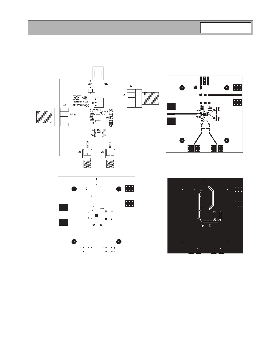
Evaluation Board Layout
Board Size 2.0" x 2.0"
Board Thickness 0.032", Board Material FR-4, Multi-layer

8-466
RF3334
Rev A5 031020
0
1.0
1.0
-1.0
10.0
10.0
-10
.0
5.0
5.0
-5.
0
2.0
2.
0
-2
.0
3.0
3.0
-3.
0
4.0
4.0
-4.
0
0.2
0.2
-0.2
0.4
0.4
-0
.4
0.6
0.
6
-0
.6
0.8
0.
8
-0
.8
LO Input, Temp = +25∞C
Swp Max
0.2GHz
Swp Min
0.05GHz
0
1.0
1.0
-1.0
10.0
10.0
-10
.0
5.0
5.0
-5.
0
2.0
2.
0
-2
.0
3.0
3.0
-3.
0
4.0
4.0
-4.
0
0.2
0.2
-0.2
0.4
0.
4
-0
.4
0.6
0.
6
-0
.6
0.8
0.
8
-0
.8
RF Input, Temp = +25∞C
Swp Max
0.2GHz
Swp Min
0.05GHz

8-467
RF3334
Rev A5 031020
LNA + AGC + Mixer Gain versus Control Voltage over
Temperature
(Freq = 100 MHz, V
CC
= 5.0 V)
-5.0
0.0
5.0
10.0
15.0
20.0
25.0
30.0
35.0
0.5
1.0
1.5
2.0
2.5
3.0
3.5
4.0
4.5
RFAGC (V)
Gain (dB)
-40∞C
+25∞C
+85∞C
LNA + AGC + Mixer + IF AMP - IIP3 versus Gain over
Temperature
(Freq = 100 MHz, V
CC
= 5.0 V)
70.0
72.0
74.0
76.0
78.0
80.0
82.0
84.0
86.0
88.0
90.0
30.0
35.0
40.0
45.0
50.0
55.0
60.0
65.0
Gain (dB)
IIP3 (dB
µ
V)
-40∞C
+25∞C
+85∞C
SSB, Cascaded Noise Figure versus Gain over
Temperature
(Freq = 100 MHz, V
CC
= 5.0 V)
0.0
5.0
10.0
15.0
20.0
25.0
30.0
35.0
25.0
30.0
35.0
40.0
45.0
50.0
55.0
60.0
65.0
Gain (dB)
Noise Figure (dB)
-40∞C
+25∞C
+85∞C
RF Input VSWR versus Frequency Across Temperature
(V
CC
= 5.0 V)
1.20
1.22
1.24
1.26
1.28
1.30
1.32
1.34
1.36
1.38
1.40
70.00
80.00
90.00
100.00
110.00
120.00
130.00
Frequency (MHz)
RF Input VSWR
-40∞C
+25∞C
+85∞C
LO Input VSWR versus Temperature Across
Temperature
(V
CC
= 5.0 V)
1.50
1.55
1.60
1.65
1.70
1.75
118.00
128.00
138.00
148.00
158.00
168.00
178.00
Frequency (MHz)
LO Input VSWR
-40∞C
+25∞C
+85∞C
8-468
RF3334
Rev A5 031020
PCB Design Requirements
PCB Surface Finish
The PCB surface finish used for RFMD's qualification process is electroless nickel, immersion gold. Typical thickness is
3
µ
inch to 8
µ
inch gold over 180
µ
inch nickel.
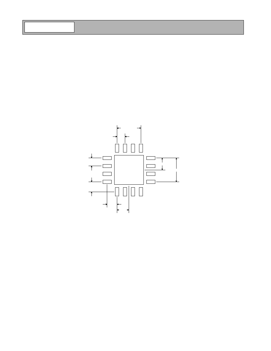
PCB Land Pattern Recommendation
PCB land patterns are based on IPC-SM-782 standards when possible. The pad pattern shown has been developed and
tested for optimized assembly at RFMD; however, it may require some modifications to address company specific
assembly processes. The PCB land pattern has been developed to accommodate lead and package tolerances.
PCB Metal Land Pattern
A = 0.69 x 0.28 (mm) Typ.
B = 0.28 x 0.69 (mm) Typ.
C = 2.40 (mm) Sq.
Dimensions in mm.
1.95 Typ.
0.65 Typ.
0.65 Typ.
0.81 Typ.
0.81 Typ.
0.98
0.98
1.95 Typ.
Pin 1
Pin 16
Pin 12
Pin 8
B
B
B
B
A
A
A
A
A
C
A
A
A
B
B
B
B
Figure 1. PCB Metal Land Pattern (Top View)
8-469
RF3334
Rev A5 031020
PCB Solder Mask Pattern
Liquid Photo-Imageable (LPI) solder mask is recommended. The solder mask footprint will match what is shown for the
PCB metal land pattern with a 2mil to 3mil expansion to accommodate solder mask registration clearance around all
pads. The center-grounding pad shall also have a solder mask clearance. Expansion of the pads to create solder mask
clearance can be provided in the master data or requested from the PCB fabrication supplier.
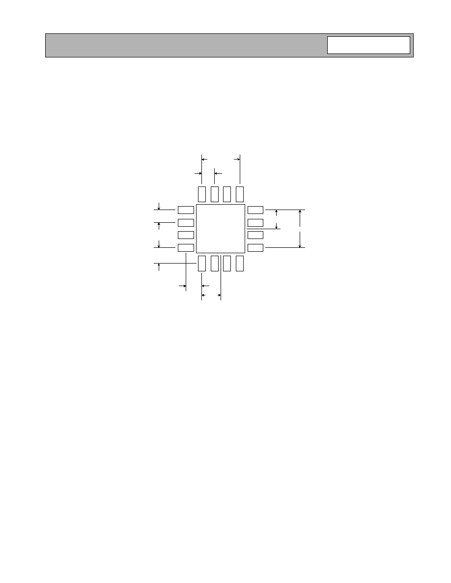
Thermal Pad and Via Design
The PCB land pattern has been designed with a thermal pad that matches the die paddle size on the bottom of the
device.
Thermal vias are required in the PCB layout to effectively conduct heat away from the package. The via pattern has been
designed to address thermal, power dissipation and electrical requirements of the device as well as accommodating
routing strategies.
The via pattern used for the RFMD qualification is based on thru-hole vias with 0.203mm to 0.330mm finished hole size
on a 0.5mm to 1.2mm grid pattern with 0.025mm plating on via walls. If micro vias are used in a design, it is suggested
that the quantity of vias be increased by a 4:1 ratio to achieve similar results.
A = 0.79 x 0.38 (mm) Typ.
B = 0.38 x 0.79 (mm) Typ.
C = 2.50 (mm) Sq.
Dimensions in mm.
1.95 Typ.
0.65 Typ.
0.65 Typ.
0.81 Typ.
0.81 Typ.
0.98
1.95 Typ.
0.98
B
B
B
B
A
A
A
A
B
B
B
B
A
A
A
A
C
Pin 1
Pin 16
Pin 12
Pin 8
Figure 2. PCB Solder Mask Pattern (Top View)

8-470
RF3334
Rev A5 031020