Preliminary
RT9173B
DS9173B-00 June 2003
www.richtek.com
1
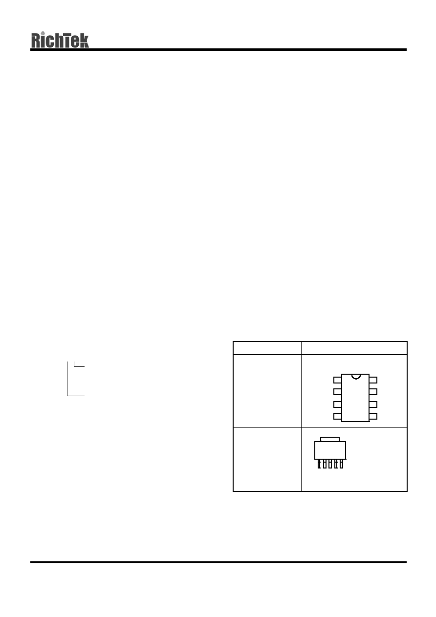
Package Type
S : SOP-8
L5 : TO-252-5
2A Bus Termination Regulator
General Description
The RT9173B regulator is designed to convert
voltage supplies ranging from 1.7V to 6V into a
desired output voltage of which adjusted by two
external voltage divider resistors. The regulator is
capable of sourcing or sinking up to 2A of current
while regulating an output voltage to within 40mV.
The RT9173B, used in conjunction with series
termination resistors, provides an excellent voltage
source for active termination schemes of high speed
transmission lines as those seen in high speed
memory buses and distributed backplane designs.
The voltage output of the regulator can be used as a
termination voltage for DDR SDRAM.
Current limits in both sourcing and sinking mode, plus
on-chip thermal shutdown make the circuit tolerant of
the output fault conditions.
The RT9173B are available in the popular 5-lead
TO-252 and fused SOP-8 (the multiple V
CNTL
pins on
the SOP-8 package are internally connected but
lowest thermal resistance) surface mount packages.
Ordering Information
RT9173B
Features
Support Both DDR I (1.25V
TT
) and DDR II
(0.9V
TT
) Requirements
SOP-8 and TO-252-5 Packages
Capable of Sourcing and Sinking Current
Current-limiting Protection
Thermal Protection
Integrated Power MOSFETs
Generates Termination Voltages for SSTL-2
High Accuracy Output Voltage at Full-Load
Adjustable V
OUT
by External Resistors
Minimum External Components
Shutdown for Standby or Suspend Mode
Operation with High-impedance Output
Applications
DDR Memory Termination Supply
Active Termination Buses
Desktop PC/AGP Graphics
Set Top Box/IPC
Supply Splitter
Pin Configurations
Part Number
Pin Configurations
RT9173BCS
(Plastic SOP-8)
TOP VIEW
RT9173BCL5
(Plastic TO-252-5)
TOP VIEW
1. VIN
2. GND
3. VCNTL (TAB)
4. REFEN
5. VOUT
Operating Temperature Range
C: Commercial Standard
1 2 3 4 5
VIN
GND
REFEN
VOUT
VCNTL
VCNTL
VCNTL
VCNTL
1
2
3
4
8
7
6
5
RT9173B
Preliminary
www.richtek.com
DS9173B-00 June 2003
2
Typical Application Circuit
Pin Description
Pin Name
Pin Function
VIN Supply
Input
GND Common
Ground
VCNTL
Gate Drive Voltage
REFEN
Reference Voltage Input and Chip Enable
VOUT Output
Voltage
Function Block Diagram
R
1
= R
2
= 100K
, R
TT
= 50
/ 33 / 25
C
OUT(min.)
= 10
�F (Ceramic) + 1000�F under the worst case test condition
R
DUMMY
= 1k
as for V
OUT
discharge when VIN is not present but V
CNTL
is present
C
IN
= 470
�F (Low ESR), C
CNTL
= 47
�F
VIN
REFEN
GND
VCNTL
VOUT
RT9173B
EN
2N7002
R
1
R
2
V
IN
= 2.5V
V
CNTL
= 3.3V
C
CNTL
C
IN
R
TT
C
OUT
R
DUMMY
Thermal
Current
Limiting Sensor
VOUT
REFEN
GND
CNTL
VIN
VCNTL
Preliminary
RT9173B
DS9173B-00 June 2003
www.richtek.com
3
Absolute Maximum Ratings
(Note 1)
Input Voltage
7V
Power Dissipation
Internally Limited
ESD Susceptibility (Note 2)
2kV
Storage Temperature Range
-65�C to 150�C
Lead Temperature (Soldering, 10 sec.)
260
�C
Package Thermal Resistance
TO-252,
JC
8
�C/W
SOP-8,
JC
15.7
�C/W
Recommended Operating Conditions
(Note 3)
Junction Temperature Range
-40�C to 125�C
Electrical Characteristics
(V
IN
= 2.5V, V
CNTL
= 3.3V, V
REFEN
= 1.25V, C
OUT
= 10
�F (Ceramic), T
A
= 25
�C unless otherwise specified)
Parameter Symbol Test
Conditions Min
Typ
Max Units
Output Offset Voltage
V
OS
I
OUT
= 0A, Fig.1 (Note 4)
-20 0 20
mV
I
L
: 0
2A, Fig.1
Load Regulation
V
LOAD
I
L
: 0A
-2A
-20 0 20
mV
V
IN
1.7
2.5/1.8
--
Input Voltage Range (DDR I/II)
V
CNTL
Keep V
CNTL
V
IN
on operation power
on and power off sequences
3 3.3/5 6
V
Operating Current of VCNTL
I
CNTL
No
Load
-- 1 2.5
mA
Current In Shutdown Mode
I
SHDN
V
REFEN
< 0.2V, R
L
= 180
, Fig.2
--
50
90
�A
Short Circuit Protection
Current limit
I
LIMIT
Fig.3,4
2.2 2.6 -- A
Over Temperature Protection
Thermal Shutdown Temperature T
SD
3.3V
V
CNTL
5V
125
170
--
�C
Thermal Shutdown Hysteresis
T
SD
3.3V
V
CNTL
5V
--
35
--
�C
Shutdown Function
Output = High, Fig.5
0.6
--
--
Shutdown Threshold Trigger
Output = Low, Fig.5
--
--
0.2
V
RT9173B
Preliminary
www.richtek.com
DS9173B-00 June 2003
4
Note 1. Stresses beyond those listed under "Absolute Maximum Ratings" may cause permanent damage to the device. These
are stress ratings only, and functional operation of the device at these or any other conditions beyond those indicated
in the operational sections of the specifications is not implied. Exposure to absolute maximum rating conditions for
extended periods may affect device reliability.
Note 2. Devices are ESD sensitive. Handling precaution recommended. The human body model is a 100pF capacitor
discharged through a 1.5K
resistor into each pin.
Note 3. The device is not guaranteed to function outside its operating conditions.
Note 4. V
OS
offset is the voltage measurement defined as V
OUT
subtracted from V
REFEN
.
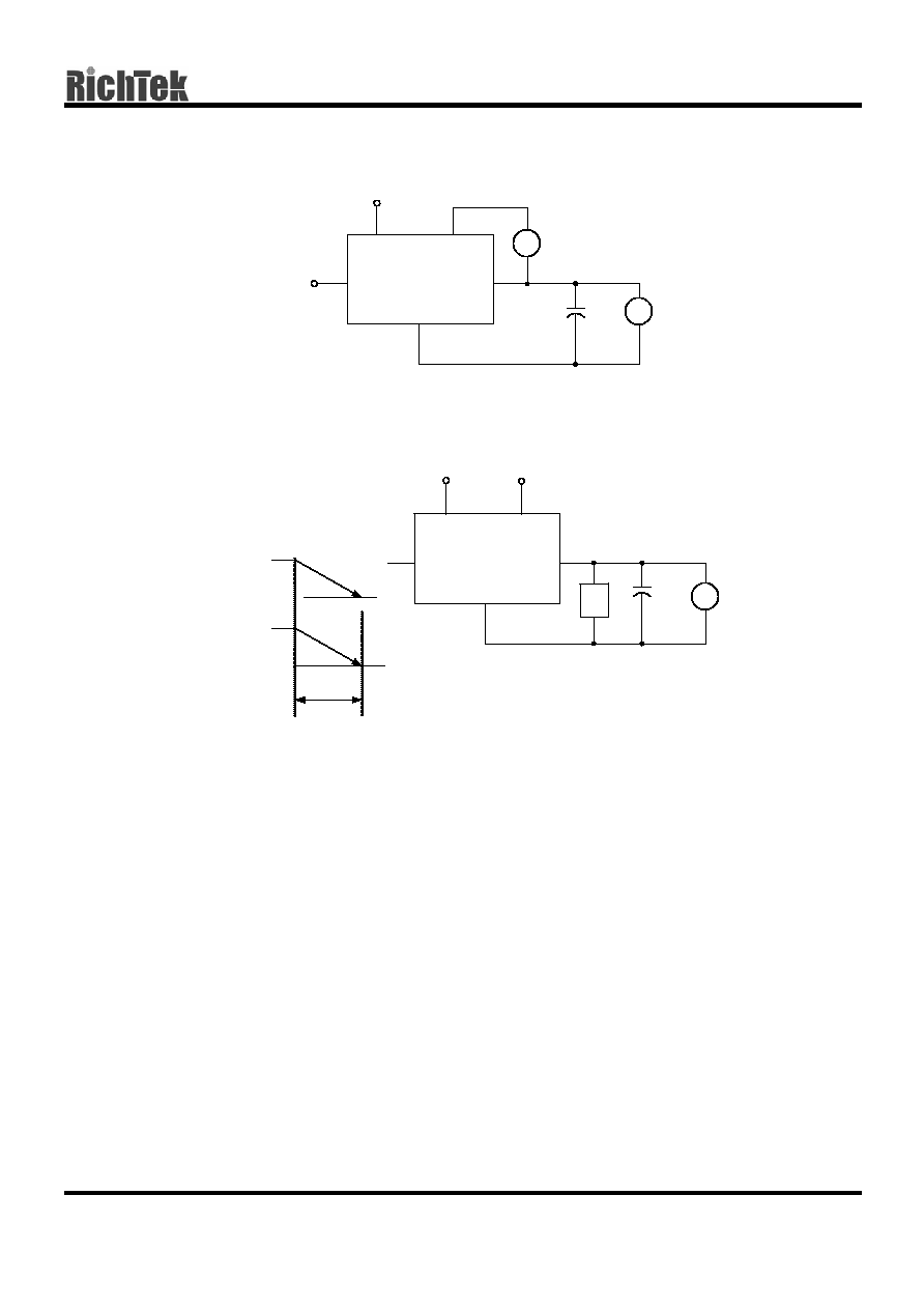
Test Circuit
Fig.1 Output Voltage Tolerance,
V
OUT
Fig.2 Current in Shutdown Mode, I
SHDN
Fig.3 Current Limit for High Side, I
CLHIGH
VIN
REFEN
GND
VCNTL
VOUT
RT9173B
2.5V
3.3V
1.25V
C
OUT
I
L
V
OUT
V
VIN
REFEN
GND
VCNTL
VOUT
RT9173B
2.5V
3.3V
1.25V
C
OUT
V
OUT
V
R
L
1.25V
0V
R
L
and C
OUT
Time deleay
0.2V
A
VCNTL
REFEN
GND
VIN
VOUT
RT9173B
3.3V
2.5V
1.25V
C
OUT
I
L
V
OUT
V
A
Preliminary
RT9173B
DS9173B-00 June 2003
www.richtek.com
5
Fig.4 Current Limit for Low Side, I
CLLOW
Fig.5 REFEN Pin Shutdown Threshold, V
TRIGGER
VCNTL
REFEN
GND
VIN
VOUT
RT9173B
2.5V
3.3V
1.25V
C
OUT
I
L
V
OUT
V
A
Power Supply
with Current Limit
VCNTL
REFEN
GND
VIN
VOUT
RT9173B
3.3V
2.5V
C
OUT
V
OUT
V
R
L
1.25V
0V
R
L
and C
OUT
Time deleay
1.25V
0.2V
V
OUT
V
REFEN
V
OUT
would be low if V
REFEN
< 0.2V
V
OUT
would be high if V
REFEN
> 0.6V