SOT23-6W 120mA 2ch LDO REGULATORS
R5322N SERIES
1
OUTLINE
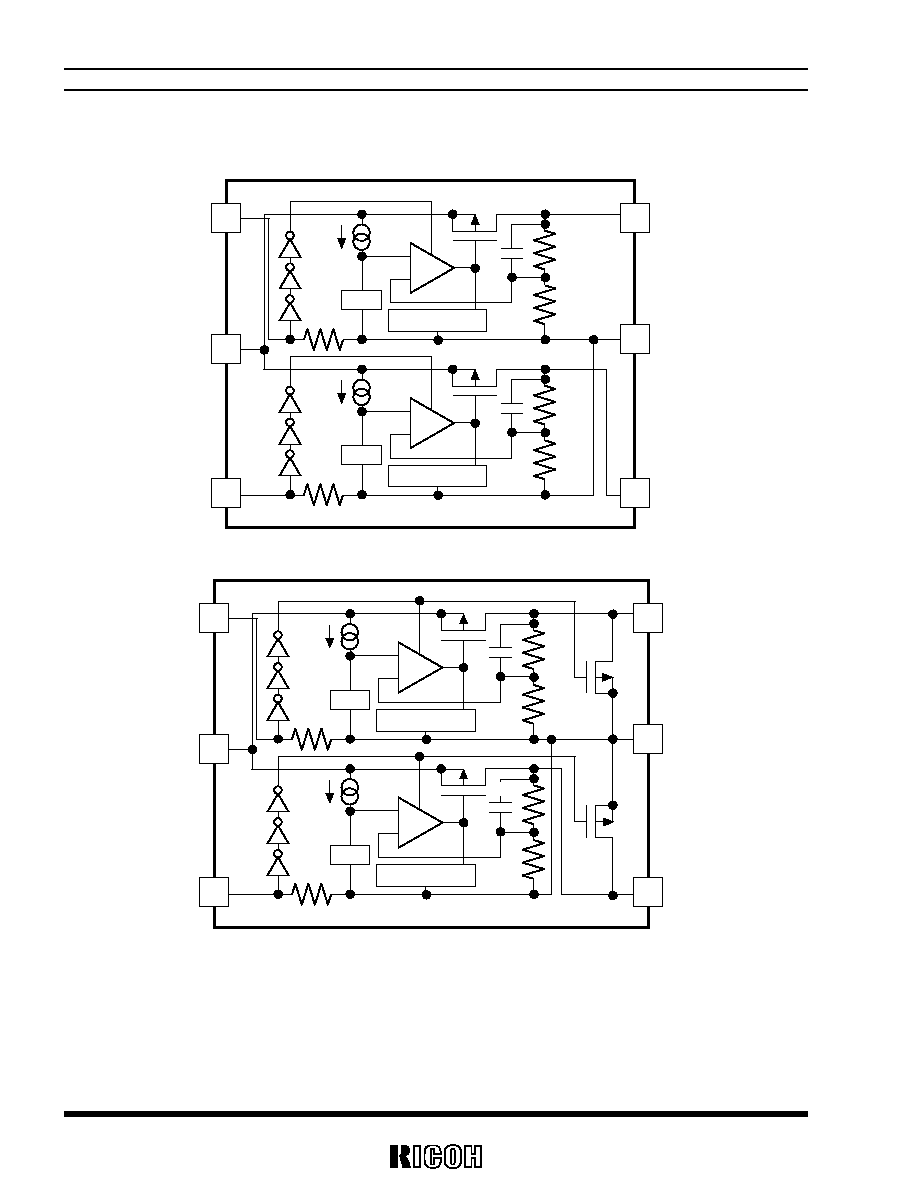
The R5322N Series are voltage regulator ICs with high output voltage accuracy, low supply current, low dropout,
and high ripple rejection by CMOS process. Each of these voltage regulator ICs consists of a voltage reference unit, an
error amplifier, resistors for setting Output Voltage, a current limit circuit, and a chip enable circuit.
These ICs perform with low dropout voltage due to built-in transistor with low ON resistance, and a chip enable
function and prolong the battery life of each system. The line transient response and load transient response of the
R5322N Series are excellent, thus these ICs are very suitable for the power supply for hand-held communication
equipment.
The output voltage of these ICs is internally fixed with high accuracy. Since the package for these ICs is SOT-23-
6W package, and include 2ch LDO regulators each, high density mounting of the ICs on boards is possible.
FEATURES
∑ Ultra-Low Supply Current ................................................. TYP. 75µA (VR1,VR2)
∑ Standby Mode..................................................................... TYP. 0.1µA (VR1,VR2)
∑ Low Dropout Voltage ......................................................... TYP. 0.15V (I
OUT
=100mA Output Voltage=3.0V Type)
∑ High Ripple Rejection ........................................................ TYP. 75dB (f=1kHz)
∑ Low Temperature-Drift Coefficient of Output Voltage..... TYP. ±100ppm/∞C
∑ Excellent Line Regulation.................................................. TYP. 0.05%/V
∑ High Output Voltage Accuracy .......................................... ±2.0%
∑ Small Package .................................................................... SOT-23-6W
∑ Output Voltage.................................................................... Stepwise setting with a step of 0.1V in the range of 1.5V to
4.0V is possible
∑ Built-in chip enable circuit (A/B: active high)
∑ Built-in fold-back protection circuit................................... TYP. 40mA (Current at short mode)
APPLICATIONS
∑ Power source for cellular phones such as GSM, CDMA and various kinds of PCS.
∑ Power source for electrical appliances such as cameras, VCRs and camcorders.
∑ Power source for battery-powered equipment.

R5322N
3
SELECTION GUIDE
The output voltage, mask option, and the taping type for the ICs can be selected at the user's request. The selec-
tion can be made with designating the part number as shown below;
R5322N◊◊◊◊-◊◊ Part Number
a b c
Code
Contents
a
Setting combination of 2ch Output Voltage (V
OUT
) : Serial Number for Voltage Setting,
Stepwise setting with a step of 0.1V in the range of 1.5V to 4.0V is possible for each channel.
b
Designation of Mask Option :
A version: without auto discharge function at OFF state.
B version: with auto discharge function at OFF state.
c
Designation of Taping Type :
Ex. TR (refer to Taping Specifications; TR type is the standard direction.)
PIN CONFIGURATION
SOT-23-6W
(mark side)
V
OUT1
GND
V
OUT2
CE1
V
DD
CE2
5
6
4
1
2
3
PIN DESCRIPTION
Pin No.
Symbol
Description
1
CE1
Chip Enable Pin 1
2
V
DD
Input Pin
3
CE2
Chip Enable Pin 2
4
V
OUT2
Output Pin 2
5
GND
Ground Pin
6
V
OUT1
Output Pin 1