'2001.7.10
SOT23-6 150mA 2ch LDO REGULATORS
R5323N SERIES
Rev. 1.10
- 1 -
s
OUTLINE
The R5323N Series are voltage regulator ICs with high output voltage accuracy, low supply current, low dropout, and high
ripple rejection by CMOS process. Each of these voltage regulator ICs consists of a voltage reference unit, an error amplifier,
resistors for setting Output Voltage, a current limit circuit, and a chip enable circuit.
These ICs perform with low dropout voltage due to built-in transistor with low ON resistance, and a chip enable function
prolongs the battery life of each system. The line transient response and load transient response of the R5323N Series are
excellent, thus these ICs are very suitable for the power supply for hand-held communication equipment.
The output voltage of these ICs is internally fixed with high accuracy. Since the package for these ICs is SOT-23-6 package,
2ch LDO regulators are included in each package, high density mounting of the ICs on boards is possible.
s
FEATURES
Low Supply Current .................................................. TYP. 90
µ
A(VR1,VR2)
Standby Mode ........................................................... TYP. 0.1
µ
A(VR1,VR2)
Low Dropout Voltage ................................................ TYP. 0.22V(I
OUT
=150mA Output Voltage=3.0V Type)
High Ripple Rejection ............................................... TYP. 75dB(V
OUT
2.4V), TYP. 70dB(V
OUT
2.5V) (f=1kHz)
........................................................................................... TYP. 65dB(V
OUT
2.4V), TYP. 60dB(V
OUT
2.5V) (f=10kHz)
Low Temperature-Drift Coefficient of Output Voltage TYP. ±100ppm/
∞
C
Excellent Line Regulation ......................................... TYP. 0.02%/V
High Output Voltage Accuracy.................................. ±2.0%
Small Package ..........................................................SOT-23-6
Output Voltage...........................................................Stepwise setting with a step of 0.1V in the range of 1.5V to 4.0V is
possible
Built-in chip enable circuit (A/B: active high)
Built-in fold-back protection circuit ..........................TYP. 40mA (Current at short mode)
Ceramic Capacitor is recommended. (1
µ
F or more)
s
APPLICATIONS
Power source for handheld communication equipment.
Power source for electrical appliances such as cameras, VCRs and camcorders.
Power source for battery-powered equipment.
Rev. 1.10
- 2 -
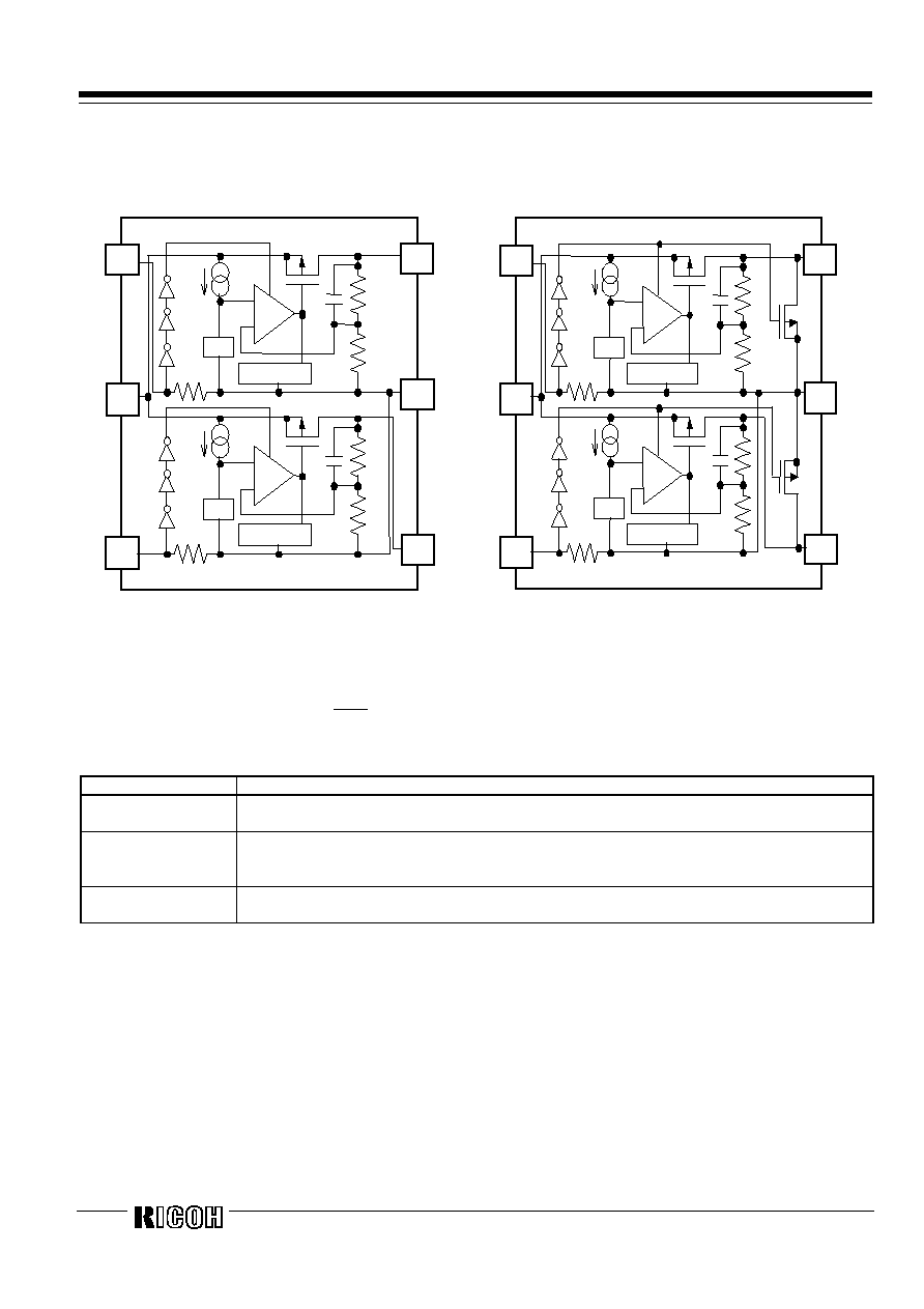
s
BLOCK DIAGRAM
R5323NXXXA
R5323NXXXB
R2_2
R1_2
R1_1
R2_1
1
3
5
6
4
2
Current Limit
Vref
Error
Amp.
Current Limit
Vref
Error
Amp.
+
-
+
-
V
DD
V
OUT2
GND
V
OUT1
CE1
CE2
R2_2
R1_2
R1_1
R2_1
1
3
5
6
4
2
Current Limit
Vref
Error
Amp.
Current Limit
Vref
Error
Amp.
+
-
+
-
V
DD
V
OUT2
GND
V
OUT1
CE1
CE2
s
SELECTION GUIDE
The output voltage, mask option, and the taping type for the ICs can be selected at the user's request. The selection can be made
with designating the part number as shown below;
R5323NXXXX-XX
Part Number
a b c
Code
Contents
a
Setting combination of 2ch Output Voltage (V
OUT
) : Serial Number for Voltage Setting,
Stepwise setting with a step of 0.1V in the range of 1.5V to 4.0V is possible for each channel.
b
Designation of Mask Option :
A version: without auto discharge function at OFF state.
B version: with auto discharge function at OFF state.
c
Designation of Taping Type :
Ex. TR (refer to Taping Specifications; TR type is the standard direction.)
Rev. 1.10
- 4 -
s
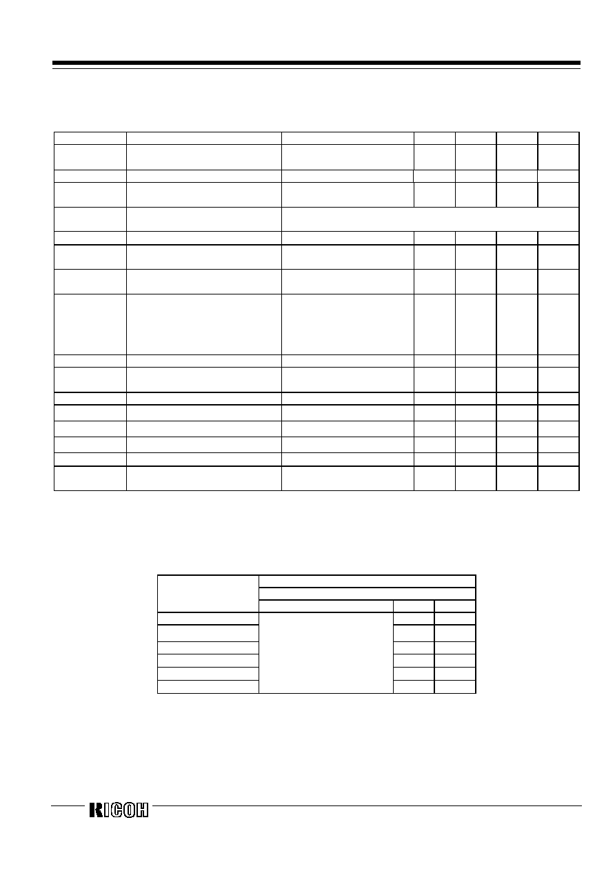
ELECTRICAL CHARACTERISTICS
q
R5323NXXXA/B
Topt=25
∞
C
Symbol
Item
Conditions
MIN.
TYP.
MAX.
Unit
V
OUT
Output Voltage
V
IN
= Set V
OUT
+1V
1mA
I
OUT
30mA
V
OUT
◊
0.98
V
OUT
◊
1.02
V
I
OUT
Output Current
V
IN
- V
OUT
= 1.0V
150
mA
V
OUT
/
I
OUT
Load Regulation
V
IN
= Set V
OUT
+1V
1mA
I
OUT
150mA
15
40
mV
V
DIF
Dropout Voltage
Refer to the ELECTRICAL CHARACTERISTICS by OUTPUT
VOLTAGE
I
SS
Supply Current
V
IN
= Set V
OUT
+1V
90
120
µ
A
Istandby
Supply Current (Standby)
V
IN
= Set V
OUT
+1V
V
CE
= GND
0.1
1.0
µ
A
V
OUT
/
V
IN
Line Regulation
Set V
OUT
+0.5V
V
IN
6V
I
OUT
= 30mA
0.02
0.10
%/V
RR
Ripple Rejection
Ripple 0.5Vp-p V
IN
= Set
V
OUT
+1V
I
OUT
= 30mA
( In case that V
OUT
1.7V,
V
IN
= Set V
OUT
+1.2V)
75
*Note1
65
*Note2
dB
V
IN
Input Voltage
2.0
6.0
V
V
OUT
/
T
Output Voltage
Temperature Coefficient
I
OUT
= 30mA
-40
∞
C
Topt
85
∞
C
±100
ppm
/
∞
C
Ilim
Short Current Limit
V
OUT
= 0V
40
mA
R
PD
CE Pull-down Resistance
0.7
2.0
8.0
M
V
CEH
CE Input Voltage "H"
1.5
V
IN
V
V
CEL
CE Input Voltage "L"
0.0
0.3
V
e
n
Output Noise
BW=10Hz to 100kHz
30
µ
Vrms
R
LOW
Low Output Nch Tr. ON
Resistance (of B version)
V
CE
=0V
60
Note1: f=1kHz, 70dB as to V
OUT
2.5V Output type.
Note2: f=10kHz, 60dB as to V
OUT
2.5V Output type.
q
ELECTRICAL CHARACTERISTICS by OUTPUT VOLTAGE
Topt = 25
∞
C
Dropout Voltage
V
DIF
(V)
Output Voltage
V
OUT
(V)
Condition
TYP.
MAX.
V
OUT
= 1.5
0.38
0.70
V
OUT
= 1.6
0.35
0.65
V
OUT
= 1.7
0.33
0.60
1.8
V
OUT
2.0
0.32
0.55
2.1
V
OUT
2.7
0.28
0.50
2.8
V
OUT
4.0
I
OUT
= 150mA
0.22
0.35
*Recommended Ceramic capacitor for Output: GRM219R61A105K(Murata)
General Example of External Components
Ceramic Capacitors: C1608X5R0J105K (TDK)
GRM188R60J105K (Murata)

Rev. 1.10
- 5 -
s
TEST CIRCUITS
C1
V
OUT
2
2
2
2
V
C3
C2
I
OUT
1
V
V
OUT
1
GND
CE1
CE2
V
OUT1
V
DD
R5323N
SERIES
V
OUT2
I
OUT
2
A
I
SS
C1
C3
C2
GND
CE1
CE2
V
OUT1
V
DD
R5323N
SERIES
V
OUT2
Fig.1 Standard test Circuit
Fig.2 Supply Current Test Circuit
Pulse
Generator
C3
C2
I
OUT
1
I
OUT
2
GND
CE1
CE2
V
OUT1
V
DD
R5323N
SERIES
V
OUT2
PG
I
OUT
1a
C1
C3
C2
I
OUT
2
b
GND
CE1
CE2
V
OUT1
VDD
R5323N
SERIES
V
OUT2
I
OUT
1b
I
OUT
2
Fig.3 Ripple Rejection, Line Transient Response Test
Circuit
Fig.4 Load Transient Response Test Circuit
s
TYPICAL APPLICATION
C3
C2
VDD
CE2
CE1
V
OUT2
GND
6
4
5
1
3
2
R5323NXXXX
SERIES
V
OUT1
OUT1
OUT2
C1
IN
(External Components) Output Capacitor; Ceramic Type