 | –≠–ª–µ–∫—Ç—Ä–æ–Ω–Ω—ã–π –∫–æ–º–ø–æ–Ω–µ–Ω—Ç: RN5RG50A | –°–∫–∞—á–∞—Ç—å:  PDF PDF  ZIP ZIP |
VOLTAGE REGULATOR WITH
EXTERNAL POWER TRANSISTOR
RN5RG SERIES
1
OUTLINE
The RN5RG Series are CMOS-based voltage regulator ICs with an external power transistor with high output
voltage accuracy and lowest supply current. Each of these voltage regulator ICs consists of a voltage reference
unit, an error amplifier and resistors.
These ICs are suitable for constructing regulators with ultra-low dropout voltage and an output current in the
range of several tens mA to several hundreds mA.
Furthermore, these ICs have a chip enable function, so that the supply current on standby can be minimized.
Since the package for these ICs is SOT-23-5 (Mini-mold) package, high density mounting of the ICs
on boards is possible.
∑ Ultra-Low Supply Current ..............................Typ. 50µA
∑ Standby Mode.....................................................Typ. 0.2µA
∑ Ultra-Low Dropout Voltage .............................Typ. 0.1V (I
OUT
=100mA : dependent on External Tr.)
∑ Low Temperature-Drift Coefficient of Output Voltage ...................Typ. ±100 ppm/∞C
∑ Excellent Line Regulation ................................Typ. 0.1%/V
∑ Output Voltage .................................................Stepwise setting with a step of 0.1V in the range of 2.0V to 6.0V is
possible (refer to Selection Guide).
∑ High Accuracy Output Voltage ........................±2.5%
∑ Small Package ..................................................SOT-23-5(Mini-Mold)
FEATURES
APPLICATIONS
∑ Power source for battery-powered equipment.
∑ Power source for cameras, VCRs, camcorders, hand-held audio instruments, and hand-held communication
equipment.
∑ Power source for domestic appliances.
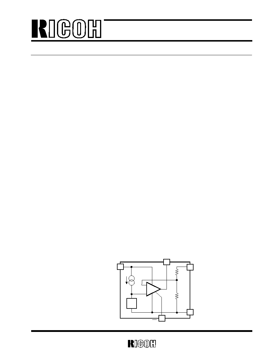
BLOCK DIAGRAM
2
5
4
3
1
Vref
V
OUT
GND
V
DD
≠
+
EXT
CE
NO. EA-020-0204
RN5RGxxxx
≠
xx
Part Number
a bc
d
RN5RG
2
SELECTION GUIDE
The output voltage, the version, the packing type, and the taping type for the ICs can be selected at the user's
request.
The selection can be made by designating the part number as shown below :
For example, the product with Output Voltage 5.0V, Version A, and Taping Type TR is designated by Part
Number RN5RG50AA-TR.
Code
Contents
Setting Output Voltage (V
OUT
):
a
Stepwise setting with a step of 0.1V in the range of 2.0V to 6.0V is possible.
b
A
Designation of Packing Type:
c
A: Taping
C: Antistatic bag for samples
Designation of Taping Type:
d
Ex. TR, TL
(refer to Taping Specifications)
"TR" is prescribed as a standard.
}
}
Absolute Maximum ratings are threshold limit values that must not be exceeded even for an instant under any
conditions. Moreover, such values for any two items must not be reached simultaneously. Operation above
these absolute maximum ratings may cause degradation or permanent damage to the device. These are stress
ratings only and do not necessarily imply functional operation below these limits.
RN5RG
3
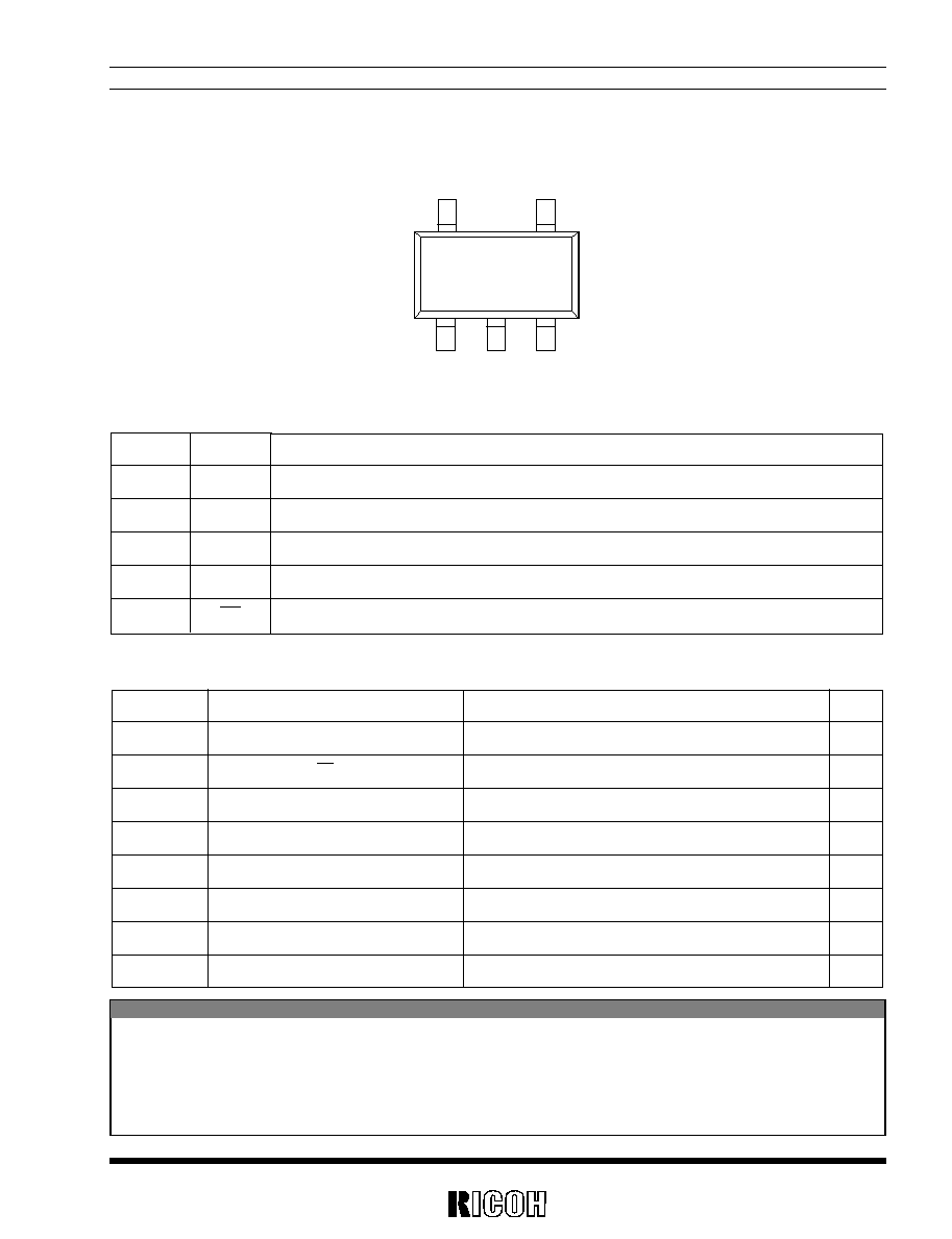
PIN CONFIGURATION
PIN DESCRIPTION
Pin No.
Symbol
1
GND
2
V
DD
3
V
OUT
4
EXT
5
CE
∑
SOT-23-5
1
2
3
5
4
(mark side)
Description
Ground Pin
Input Pin
Output Pin
External Transistor Drive Pin (Nch Open Drain Output)
Chip Enable Pin
ABSOLUTE MAXIMUM RATINGS
Symbol
Item
V
IN
Input Voltage
V
CE
Input Voltage (CE Pin)
V
EXT
EXT Output Voltage
I
EXT
EXT Output Current
P
D
Power Dissipation
Topt
Operating Temperature Range
Tstg
Storage Temperature Range
Tsolder
Lead Temperature (Soldering)
Rating
Unit
+12
V
≠ 0.3 to V
IN
+0.3
V
+12
V
50
mA
150
mW
≠ 40 to +85
∞C
≠ 55 to +125
∞C
260∞C,10s
ABSOLUTE MAXIMUM RATINGS
RN5RG
4
ELECTRICAL CHARACTERISTICS
Symbol
Item
V
OUT
Output Voltage
I
OUT
Output Current
I
EXT
EXT Current
V
OUT
Load Regulation
I
OUT
V
DIF
Dropout Voltage
I
SS
Supply Current
Istandby
Supply Current (Standby)
I
EXT
leak
EXT Leakage Current
V
OUT
V
IN
Line Regulation
V
IN
Input Voltage
V
EXT
EXT Output Voltage
V
OUT
Output Voltage
Topt
Temperature Coefficient
V
CEH
CE Input Voltage "H"
V
CEL
CE Input Voltage "L"
I
CEH
CE Input Current "H"
I
CEL
CE Input Current "L"
Conditions Min.
Typ.
Max.
Unit
Note
V
IN
=8.0V
V
OUT
V
OUT
V
I
OUT
=50mA
◊
0.975
◊
1.025
V
IN
≠V
OUT
=1.0V
1000
mA
Note
V
IN
=4.0V, V
EXT
=2.0V
10
mA
V
IN
≠V
OUT
=1.0V
1mA
I
OUT
100mA
≠60
60
mV
I
OUT
=100mA
100
200
mV
V
IN
≠V
OUT
=1.0V
I
OUT
=0mA (at no load)
50
80
µA
V
IN
=8V
0.01
0.20
1.00
µA
0.5
µA
I
OUT
=50mA
0.0
0.1
0.3
%/V
V
OUT
+0.5V
V
IN
8V
8
V
8
V
I
OUT
=10mA
≠40∞C
Topt85∞C
±100
ppm/∞C
1.5
V
0.25
V
0.0
0.1
µA
≠5.0
≠3.0
≠0.1
µA
Topt=25∞C
(Note) The output current depends upon the performance of External PNP Transistor. Use External PNP Transistor of a low saturation type, with an h
FE
of 100 or more.
*
) With respect to Test Circuits, refer to the Typical Application.

RN5RG
5
OPERATION
V
OUT
GND
GND
Vref
V
DD
External PNP Transistor
EXT
OUT
IN
RA
RB
CE
+
≠
2
4
3
Error
Amplifier
5
1
In these ICs, the output voltage V
OUT
is detected by
feed-back registers RA, RB, and the detected the output
voltage is compared with a reference voltage by error
Amplifier, so that the base current of an external PNP
transistor is adjusted and the output voltage V
OUT
is reg-
ulated.
SELECTION GUIDE FOR EXTERNAL COMPONENTS
V
OUT
C
L
V
IN
External PNP Transistor
EXT
OUT
R1
R2
3
4
Select an external PNP transistor from the view-
points of output current, input voltage and power dis-
sipation.
Generally external PNP transistor with low V
CE
(
SAT
)
and high h
FE
is suitable.
1.External PNP Transistor
EXT Pin of these ICs is protected by a current limit circuit from the destruction caused by excess current.
However, since this current limit circuit is provided for the purpose of protecting the IC, use a resistor R2 for the
protection of the External Transistor, although this IC can be operated without such a resistor. It is required that
the resistance of the Resistor R2 be determined with the input voltage, output voltage,output current, tempera-
ture, and the h
FE
value taken into consideration and the dispersion of these values. Before making such a deter-
mination, check the characteristics by calculating the respective values by using the following formula :
V
IN
[Min.] ≠1.2(V)
≠
0.7(V)
>
I
OUT
[Max.]
R2
R1
h
FE
2.Base Resistor R2
In these ICs, phase compensation is made for securing stable operation even when the load current is varied.
For this purpose, be sure to use a capacitor C
L
(tantalum type) with a capacitance of 10µF or more and a resistor
R1 with a resistance of about 10k
between the base and the emitter.There may be the case the loop oscillation
takes place when a tantalum capacitor C
L
with a large ESR is used, so select the C
L
carefully including the fre-
quency characteristics.
3.Phase Compensation
RN5RG
6
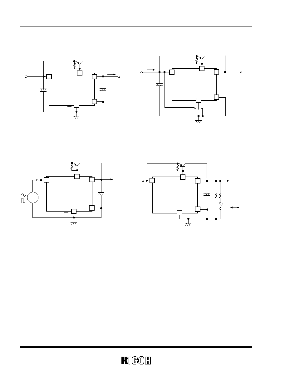
TEST CIRCUITS
Test Circuit 1 : Typical Characteristics 1) to 4)
Test Circuit 2 : Typical Characteristics 5) to 7)
Test Circuit 3 : Typical Characteristics 8) to 10)
Test Circuit 4 : Typical Characteristics 11)
I
OUT
V
OUT
GND
V
DD
EXT
RN5RG SERIES
2SA1213
PNP
OUT
IN
CE
2
4
5
1
3
10k
10 µF
10 µF
V
OUT
GND
V
DD
EXT
RN5RG SERIES
2SA1213
PNP
Oscilloscope
IN
CE
C
L
2
4
5
1
3
10k
P.G.
I
SS
GND
V
OUT
V
DD
EXT
RN5RG SERIES
2SA1213
PNP
OUT
IN
CE
(2)
(1)
10k
2
4
5
1
10
µF
3
1µF
10mA
300mA
V
OUT
GND
V
DD
EXT
RN5RG SERIES
2SA1213
PNP
Oscilloscope
IN
CE
2
4
5
1
3
10k
RN5RG
7
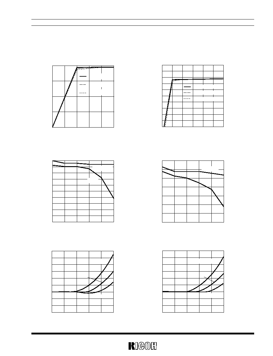
TYPICAL CHARACTERISTICS
1) Output Voltage vs. Input Voltage
RN5RG50A
RN5RG30A
RN5RG50A
2) Output Voltage vs.Output Current
RN5RG50A
RN5RG30A
3) Dropout Voltage vs. Output Curret
RN5RG30A
3.0
4.0
5.0
6.0
7.0
8.0
3.0
3.5
4.0
4.5
5.0
Input Voltage V
IN
(V)
Output Voltage V
OUT
(V)
Topt=25∞C
I
OUT
=0mA
I
OUT
=100mA
I
OUT
=500mA
Output Current I
OUT
(mA)
Dropout Voltage V
DIF
(V)
0
200
400
600
800
1000
0.00
0.05
0.10
0.15
0.20
0.25
0.30
0.35
0.40
0.45
Topt=85∞C
≠40∞C
25∞C
2
3
4
5
6
7
8
2.2
2.3
2.4
2.5
2.6
2.7
2.8
2.9
3.0
3.1
3.2
Input Voltage V
IN
(V)
Output Voltage V
OUT
(V)
Topt=25∞C
I
OUT
=0mA
I
OUT
=100mA
I
OUT
=500mA
0
100
200
300
400
500
Output Current I
OUT
(mA)
2.960
2.962
2.964
2.966
2.968
2.970
2.972
2.974
Output Voltage V
OUT
(V)
Topt=25∞C
V
IN
=4.0V
3.1V
Output Current I
OUT
(mA)
Dropout Voltage V
DIF
(V)
0
200
400
600
800
1000
0.00
0.05
0.10
0.15
0.20
0.25
0.30
0.35
0.40
0.45
Topt=85∞C
≠40∞C
25∞C
0
100
200
300
400
500
Output Current I
OUT
(mA)
4.942
4.944
4.946
4.948
4.950
4.952
4.954
4.956
4.958
4.960
4.962
Output Voltage V
OUT
(V)
Topt=25∞C
V
IN
=6.0V
5.1V
RN5RG
8
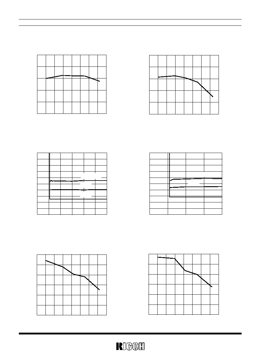
4) Output Voltage vs.Temperature
5) Supply Current vs. Input Voltage
6) Supply Current vs. Temperature
V
IN
=4V,I
OUT
=10mA
0
2.95
2.97
2.99
3.01
3.03
3.05
20
40
60
80 100
-20
-40
-60
Temperature Topt (∞C)
Output Voltage Vout (V)
RN5RG30A
V
IN
=6V,I
OUT
=10mA
0
5
5.02
5.04
5.06
5.08
5.1
20
40
60
80 100
-20
-40
-60
Temperature Topt (∞C)
Output Voltage Vout (V)
RN5RG50A
Input Voltage V
IN
(V)
Supply Current Iss(
µ
A)
I
OUT
=0mA
3
4
6
7
5
0
10
20
30
40
50
60
70
80
90
100
8
2
RN5RG30A
Topt=-40∞C
25∞C
85∞C
V
IN
=4V,I
OUT
=0mA
Supply Current Iss(
µ
A)
0
60
50
40
30
20
10
RN5RG30A
0
20
40
60
80
100
-20
-40
-60
Temperature Topt (∞C)
Supply Current Iss(
µ
A)
V
IN
=6V,I
OUT
=0mA
0
60
50
40
30
20
10
RN5RG50A
0
20
40
60
80 100
-20
-40
-60
Temperature Topt (∞C)
Input Voltage V
IN
(V)
Supply Current Iss(
µ
A)
I
OUT
=0mA
4
6
7
5
0
10
20
30
40
50
60
70
80
90
100
8
RN5RG50A
Topt=-40∞C
25∞C
85∞C
RN5RG
9
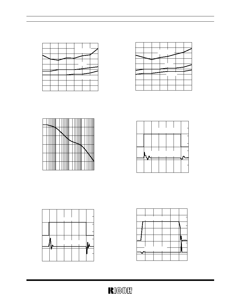
7) Standby Current vs. Input Voltage
9) Line Transient Response (1)
8) Ripple Rejection
10) Line Transient Response (2)
11) Load Transient Response
Standby Current Istandby(
µ
A)
0
0.15
0.4
0.35
0.3
0.25
0.2
0.45
0.1
0.05
RN5RG30A
1
2
8
7
6
5
4
3
Temperature Topt (∞C)
Topt=85∞C
≠40∞C
25∞C
Standby Current Istandby(
µ
A)
0
0.15
0.4
0.35
0.3
0.25
0.2
0.45
0.1
0.05
RN5RG30A
1
2
8
7
6
5
4
3
Temperature Topt (∞C)
Topt=85∞C
≠40∞C
25∞C
Input Voltage V
IN
(V)
20
40
60
80 100 120 140
0
4
5
6
7
8
I
OUT
=10mA
Topt=25∞C
Output Voltage Deviation V
OUT
(V)
≠20
≠10
0
10
20
30
40
50
Time t(µs)
C
L
=1µF
Input Voltage
Output Voltage
RN5RG50A
Output Current I
OUT
(mA)
4
8
12
16
20
24 140
0
V
IN
=6.0V
Topt=25∞C
Output Voltage Deviation V
OUT
(mV)
≠100
≠300
≠200
≠100
0
100
200
300
400
500
0
100
200
300
400
500
Time t(ms)
C
L
=1µF
Output Current
Output Voltage
RN5RG50A
10
100
1k
10k 100k
Frequency f(Hz)
0
10
20
30
40
50
60
Ripple Rejection RR(dB)
Topt=25∞C
C
L
=10 µF
I
OUT
=200mA
V
IN
=6Vdc+0.5(p-p)
RN5RG50A
Input Voltage V
IN
(V)
20
40
60
80 100 120 140
0
4
5
6
7
8
I
OUT
=100mA
Topt=25∞C
Output Voltage Deviation V
OUT
(mV)
≠20
≠10
0
10
20
30
40
50
Time t(µs)
C
L
=1µF
Input Voltage
Output Voltage
RN5RG50A

RN5RG
10
TYPICAL APPLICATION
PNP Tr
OUT
IN
EXT
CE
GND
Cap.
+
Cap.
+
V
OUT
V
DD
RN5RG SERIES
Parts Transistor : 2SA1213
Resistor : 10k
Capacitor : 10µF(tantalum type)