 | –≠–Ľ–Ķ–ļ—ā—Ä–ĺ–Ĺ–Ĺ—č–Ļ –ļ–ĺ–ľ–Ņ–ĺ–Ĺ–Ķ–Ĺ—ā: RN5RY381A | –°–ļ–į—á–į—ā—Ć:  PDF PDF  ZIP ZIP |
VFM STEP-UP DC/DC
CONVERTER CONTROLLER
RN5RYxx1 SERIES
1
OUTLINE
The RN5RYxx1 Series are CMOS-based VFM Control ICs for step-up DC/DC converter with an external dri-
ver transistor featuring high output voltage accuracy and low supply current. Each of the RN5RYxx1 Series ICs
consists of a voltage reference unit, an error amplifier, an oscillator, a VFM control circuit and feed back resistors.
A low ripple, high efficiency step -up DC/DC converter can be composed of the RN5RYxx1 Series with only an
inductor, a diode, a capacitor, and a drive transistor.
Since the package for these ICs is SOT-23-5( Mini-mold)package, high density mounting of the ICs on boards
is possible.
∑
Low Supply Current ..................................................................................Typ. 3ĶA
∑
Low Standby Current ..................................................................................Typ. 0.6ĶA
∑
Low Temperature-Drift Coefficient of Output Voltage ...........................Typ. Ī50ppm / įC
∑
High Accuracy Output Voltage ...................................................................Ī2.5%
∑
Low Oscillation Start-up Voltage ...............................................................Max. 0.8V
∑
Small Package .............................................................................................SOT-23-5(Mini-Mold)
FEATURES
APPLICATIONS
∑
Power source for battery-powered instruments.
∑
Power source for cameras, VCRs, camcorders, pagers, and other hand-held communication instruments.
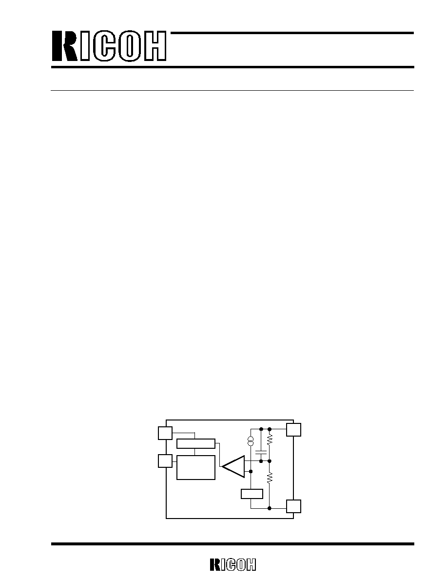
BLOCK DIAGRAM
+
≠
5
3
1
2
Vref
OSC
Output
Buffer
CE
EXT
V
OUT
GND
NO. EA-030-0204
RN5RYxx1
2
Designation of Output Voltage (V
OUT
)
V
OUT
can be designated within the range of 2.0 to 6.0V
Code
RN5RYxxxx
≠
xx
Part Number
a bc
d
SELECTION GUIDE
In the RN5RYxx1 Series, the output voltage, the version and the taping type for the ICs can be selected at
the user's request. The selection can be made by designating the part number as shown below :
}
For example, the product with Output Voltage 2.0V, Taping Type TR, is designated by Part Number
RN5RY201A ≠TR.
a
b
1
c
Designation of Packing Type:
A: Taping
C: Antistatic bag for samples
d
Designation of Taping Type:
Ex. SOT-23-5: TR, TL
(refer to Taping Specification)
"TR" is prescribed as a standard
Contents
}
RN5RYxx1
3
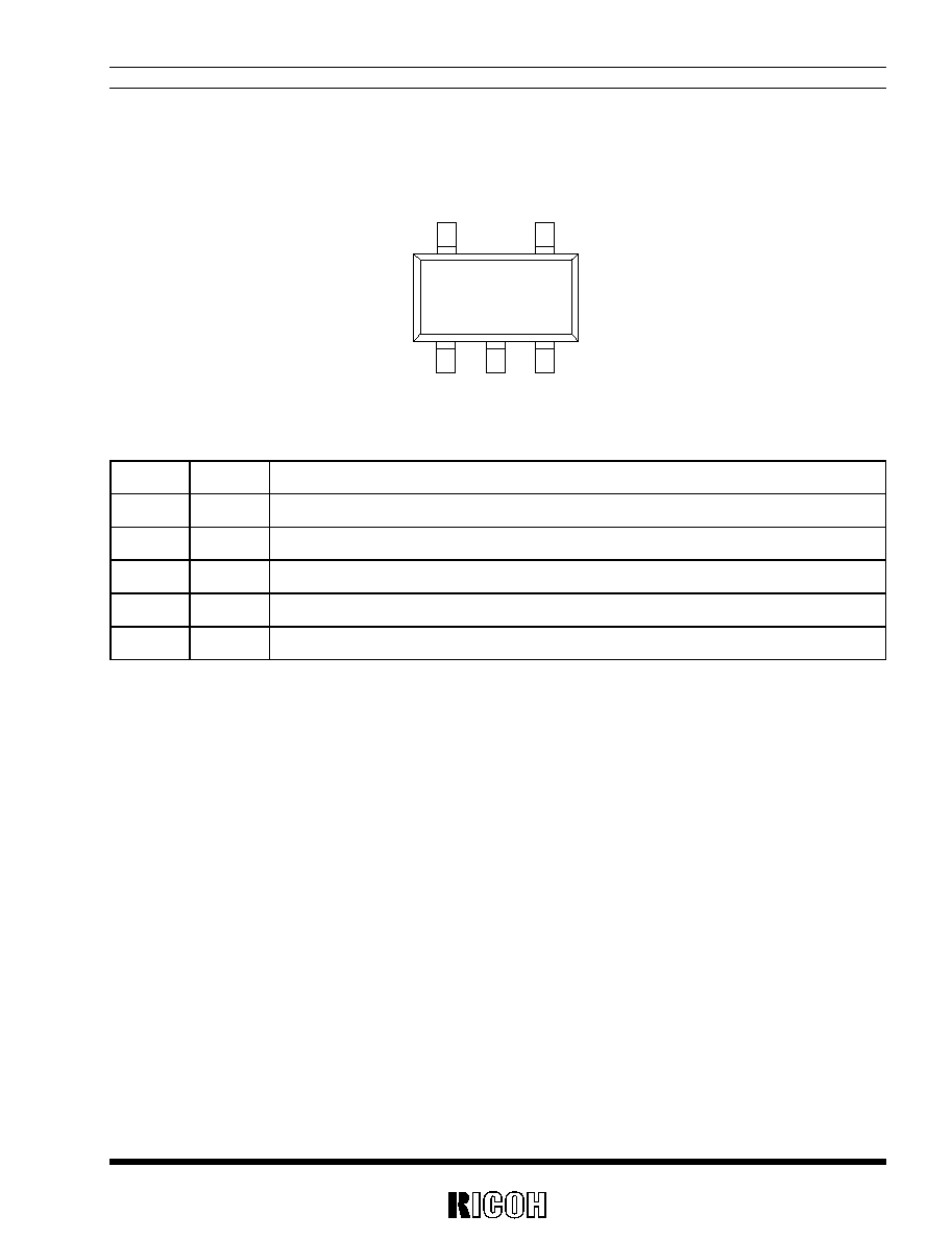
Ground Pin
Pin No.
PIN CONFIGURATION
PIN DESCRIPTION
∑
SOT-23-5
1
2
3
5
4
(mark side)
Symbol
Description
1
GND
2
V
OUT
Output Pin
3
EXT
External Transistor Drive Pin (CMOS Output)
4
NC
No Connection
5
CE
Chip Enable Pin
RN5RYxx1
4
Symbol
ABSOLUTE MAXIMUM RATINGS
Item
Ratings
Unit
V
IN
Input Voltage
+12
V
V
CE
CE Pin Input Voltage
≠0.3 to V
OUT
+0.3
V
V
EXT
EXT Pin Output Voltage
≠0.3 to V
OUT
+0.3
V
I
EXT
EXT Pin Output Current
Ī50
mA
P
D
Power Dissipation
150
≠ 30 to +85
mW
Topt
Operating Temperature
įC
≠ 55 to +125
Tstg
Storage temperature
įC
260įC, 10s
Tsolder
Lead Temperature (Soldering)
Absolute Maximum ratings are threshold limit values that must not be exceeded even for an instant under any
conditions. Moreover, such values for any two items must not be reached simultaneously. Operation above
these absolute maximum ratings may cause degradation or permanent damage to the device. These are stress
ratings only and do not necessarily imply functional operation below these limits.
ABSOLUTE MAXIMUM RATINGS
RN5RYxx1
5
Symbol
ELECTRICAL CHARACTERISTICS
∑ RN5RY301
Topt=25įC
Item
Conditions
Min.
Typ.
Max.
Unit
V
OUT
Output Voltage
V
IN
=1.5V,I
OUT
=10mA
2.925
3.000
3.075
V
V
IN
Input Voltage
10
5
V
I
DD1
Supply Current 1
EXT No load, V
OUT
=3.15V, Test circuits1
3
ĶA
50
I
DD2
Supply Current 2
EXT No load, V
OUT
=2.85V, Test circuits1
25
ĶA
1.5
Istandby
Standby Current
V
OUT
=1.5V, Test circuits2
0.6
ĶA
fosc
Maximum Oscillator Frequency
V
OUT
=2.85V, Test circuits3
180
kH
Z
Duty
Oscillator Duty Cycle
V
OUT
=2.85V, EXT High side, Test circuits3
60
75
%
0.8
Vstart
I
EXTH
Oscillator Start -Up Voltage
EXT No load, Test circuits4
0.7
V
V
OUT
Topt
Output Voltage
Temperature Coefficient
EXT "H" Output Current
I
OUT
=10mA
≠ 30įC
Topt85įC
V
OUT
=2.85V, V
EXT
=GND, Test circuits5
Ī50
ppm/įC
≠1.5
mA
I
EXTL
EXT "L" Output Current
V
OUT
=2.85V, V
EXT
=2.85V, Test circuits6
1.5
mA
V
CEH
CE "H" Input Voltage
V
OUT
=2.85V, Test circuits4
1.5
V
V
CEL
CE "L" Input Voltage
V
OUT
=2.85V, Test circuits4
0.25
V
I
CEH
CE "H" Input Current
CE=3.0V, Test circuits7
0.1
0.0
ĶA
I
CEL
CE "L" Input Current
CE=GND, Test circuits8
≠ 0.1
0.0
ĶA
RN5RYxx1
6
Symbol
∑ RN5RY401
Topt=25įC
Item
Conditions
Min.
Typ.
Max.
Unit
V
IN
Input Voltage
10
5
V
I
DD1
Supply Current 1
EXT No load, V
OUT
=4.2V, Test circuits1
3
ĶA
90
I
DD2
Supply Current 2
EXT No load, V
OUT
=3.8V, Test circuits1
50
ĶA
1.5
Istandby
Standby Current
V
OUT
=2.0V, Test circuits2
0.6
ĶA
fosc
Maximum Oscillator Frequency
V
OUT
=3.8V, Test circuits3
180
kH
Z
Duty
Oscillator Duty Cycle
V
OUT
=3.8V, EXT High side, Test circuits3
60
75
%
0.8
Vstart
Oscillator Start-Up Voltage
EXT No load, Test circuits4
0.7
V
V
OUT
Topt
Output Voltage
Temperature Coefficient
I
OUT
=10mA
≠30įC
Topt85įC
Ī50
ppm/įC
≠1.5
I
EXTH
EXT "H" Output Current
V
OUT
=3.8V, V
EXT
=GND, Test circuits5
mA
I
EXTL
EXT "L" Output Current
V
OUT
=3.8V, V
EXT
=3.8V, Test circuits6
1.5
mA
V
CEH
CE "H" Input Voltage
V
OUT
=3.8V, Test circuits4
1.5
V
0.25
V
CEL
CE "L" Input Voltage
V
OUT
=3.8V, Test circuits4
V
0.1
I
CEH
CE "H" Input Current
CE=4.0V, Test circuits7
0.0
ĶA
I
CEL
CE "L" Input Current
CE=GND, Test circuits8
≠0.1
0.0
ĶA
V
OUT
Output Voltage
V
IN
=2.0V, I
OUT
=10mA
3.900
4.000
4.100
V
RN5RYxx1
7
Symbol
∑ RN5RY501
Topt=25įC
Item
Conditions
Min.
Typ.
Max.
Unit
V
IN
Input Voltage
10
V
I
DD1
Supply Current 1
EXT No load, V
OUT
=5.25V, Test circuits1
3
5
ĶA
I
DD2
Supply Current 2
EXT No load, V
OUT
=4.75V, Test circuits1
90
150
ĶA
Istandby
Standby Current
V
OUT
=2.5V, Test circuits2
0.6
1.5
ĶA
fosc
Maximum Oscillator Frequency
V
OUT
=4.75V, Test circuits3
180
kH
Z
Duty
Oscillator Duty Cycle
V
OUT
=4.75V, EXT High side, Test circuits3
60
75
%
V
start
Oscillator Start-Up Voltage
EXT No load, Test circuits4
0.7
0.8
V
V
OUT
Topt
Output Voltage
Temperature Coefficient
I
OUT
=10mA
≠30įC
Topt85įC
Ī50
ppm/įC
I
EXTH
EXT "H" Output Current
V
OUT
=4.75V, V
EXT
=GND, Test circuits5
≠1.5
mA
I
EXTL
EXT "L" Output Current
V
OUT
=4.75V, V
EXT
=4.75V, Test circuits6
1.5
mA
V
CEH
CE "H" Input Voltage
V
OUT
=4.75V, Test circuits4
1.5
V
V
CEL
CE "L" Input Voltage
V
OUT
=4.75V, Test circuits4
0.25
V
I
CEH
CE "H" Input Current
CE=5.0V, Test circuits7
0.0
0.1
ĶA
I
CEL
CE "L" Input Current
CE=GND, Test circuits8
≠0.1
0.0
ĶA
V
OUT
Output Voltage
V
IN
=2.5V, I
OUT
=10mA
4.875
5.000
5.125
V
RN5RYxx1
8
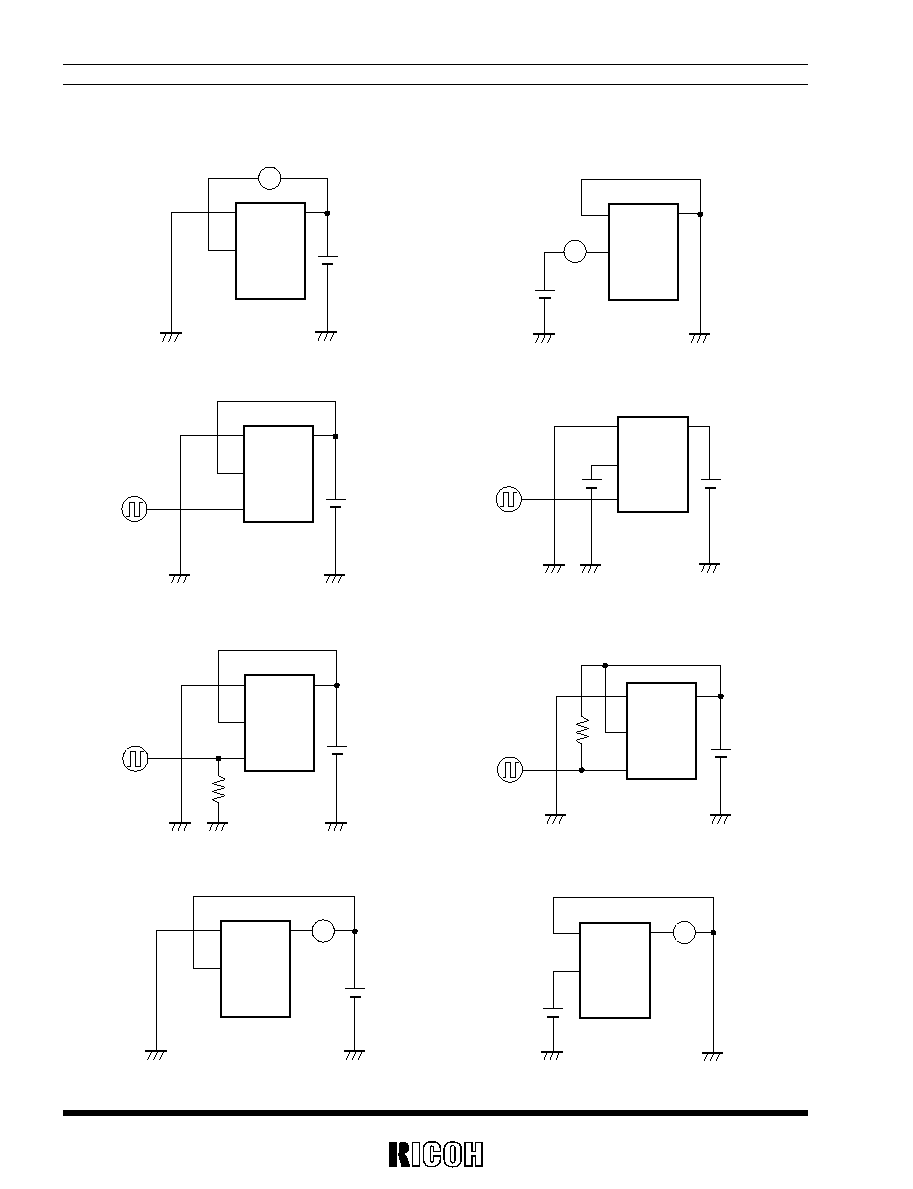
TEST CIRCUIT
Oscilloscope
Oscilloscope
GND
EXT
NC
GND
EXT
NC
GND
V
OUT
EXT
NC
CE
A
Oscilloscope
GND
EXT
NC
GND
EXT
NC
A
Oscilloscope
GND
EXT
NC
GND
EXT
NC
A
GND
EXT
NC
A
V
OUT
CE
V
OUT
CE
V
OUT
CE
V
OUT
CE
V
OUT
CE
V
OUT
CE
V
OUT
CE
Test Circuit 1
Test Circuit 4
Test Circuit 2
Test Circuit 5
Test Circuit 3
Test Circuit 7
Test Circuit 6
Test Circuit 8
RN5RYxx1
9
4.00
3.00
2.00
0
100
200
300
400
500
Output Current I
OUT
(mA)
Output Voltage V
OUT
(V)
0.8V
0.9V
1.0V
1.5V
V
IN=
2.0V
L=27
ĶH
RN5RY301
4.00
3.00
2.00
0
100
200
300
400
500
Output Current I
OUT
(mA)
0.8V
0.9V
1.0V
1.5V
V
IN=
2.0V
L=68
ĶH
RN5RY301
Output Voltage V
OUT
(V)
5.00
4.00
3.00
0
100
200
300
400
500
600
Output Current I
OUT
(mA)
Output Voltage V
OUT
(V)
L=27
ĶH
RN5RY401
0.9V
0.8V
1.0V
2.0V
V
IN=
3.0V
3.00
4.00
5.00
0
100
200
300
400
500
600
Output Current I
OUT
(mA)
L=68
ĶH
RN5RY401
0.9V
1.0V
2.0V
V
IN=
3.0V
0.8V
Output Voltage V
OUT
(V)
6.00
5.00
4.00
0
100
200
300
400
500
600
700
Output Current I
OUT
(mA)
Output Voltage V
OUT
(V)
L=27
ĶH
RN5RY501
0.8V
0.9V
1.0V
2.0V
3.0V
V
IN=
4.0V
Output Current I
OUT
(mA)
6.00
5.00
4.00
0
100
200
300
400
500
600
700
L=68
ĶH
RN5RY501
0.8V
0.9V
1.0V
2.0V
3.0V
V
IN=
4.0V
Output Voltage V
OUT
(V)
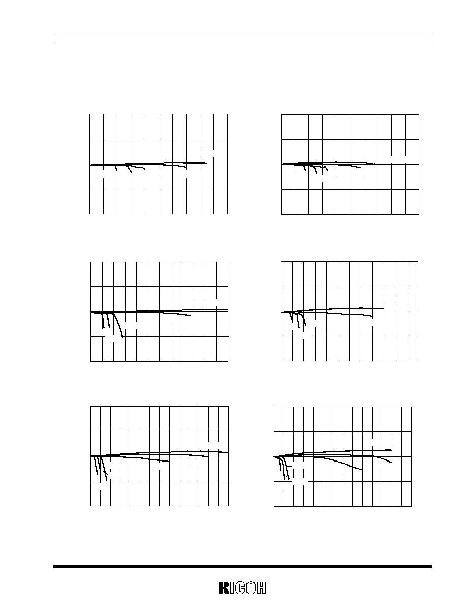
TYPICAL CHARACTERISTICS
1) Output Voltage vs. Output Current
RN5RYxx1
10
0
0
100
200
300
400
500
Output Current I
OUT
(mA)
Effciency
(%)
L=27
ĶH
RN5RY301
10
20
30
40
50
60
70
80
90
100
0.8V
1.0V
1.5V
V
IN=
2.0V
0.9V
0
0
100
200
300
400
500
Output Current I
OUT
(mA)
Effciency
(%)
L=68
ĶH
RN5RY301
10
20
30
40
50
60
70
80
90
100
1.0V
V
IN=
2.0V
0.8V
0.9V
1.5V
0
0
100
200
300
400
500
600
Output Current I
OUT
(mA)
Effciency
(%)
L=27
ĶH
RN5RY401
0.8V
10
20
30
40
50
60
70
80
90
100
0.9V
1.0V
2.0V
V
IN
=3.0V
0
0
100
200
300
400
500
600
Output Current I
OUT
(mA)
Effciency
(%)
L=68
ĶH
RN5RY401
10
20
30
40
50
60
70
80
90
100
0.8V
0.9V
1.0V
2.0V
V
IN
=3.0V
0
0
100
200
300
400
500
600
700
Output Current I
OUT
(mA)
Effciency
(%)
L=27
ĶH
RN5RY501
10
20
30
40
50
60
70
80
90
100
3.0V
V
IN
=4.0V
0.8V
0.9V
1.0V
2.0V
0
0
Output Current I
OUT
(mA)
Effciency
(%)
L=68
ĶH
RN5RY501
10
20
30
40
50
60
70
80
90
100
100
200
300
400
500
600
700
0.8V
0.9V
1.0V
2.0V
3.0V
V
IN
=4.0V
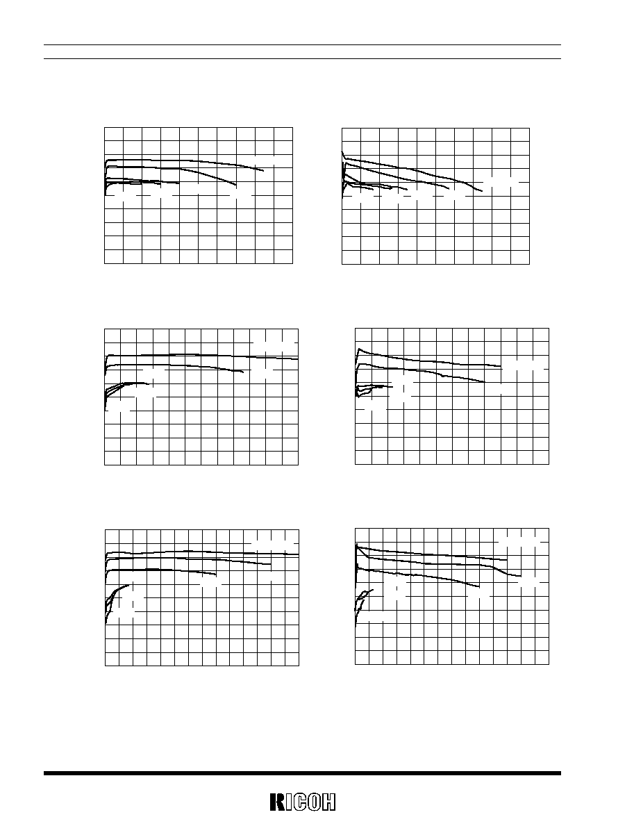
2) Efficiency vs. Output Current
RN5RYxx1
11
0
0
Output Current I
OUT
(mA)
Ripple Voltage Vr(mVp-p)
L=27
ĶH
RN5RY301
100
200
300
400
500
50
100
150
200
250
300
350
0.8V
0.9V
V
IN
=2.0V
1.0V
1.5V
0
0
Output Current I
OUT
(mA)
Ripple Voltage Vr(mVp-p)
L=27
ĶH
RN5RY401
100
200
300
400
100
200
300
400
500
600
0.8V
0.9V
2.0V
V
IN=
3.0V
1.0V
0
100
200
300
400
500
0
Output Current I
OUT
(mA)
Ripple Voltage Vr(mVp-p)
L=27
ĶH
RN5RY501
100
200
300
400
500
600
700
0.8V
0.9V
1.0V
2.0V
3.0V
V
IN=
4.0V
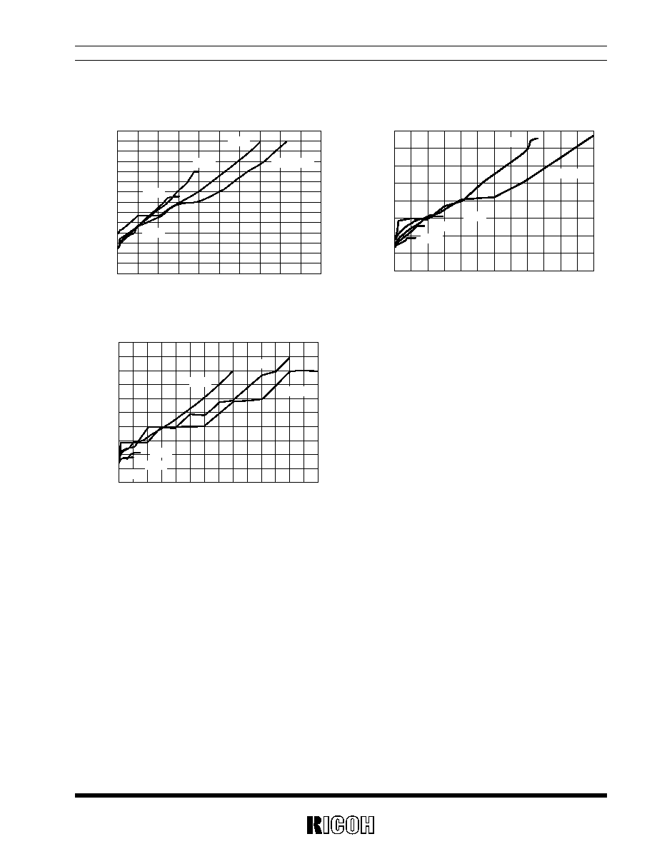
3) Ripple Voltage vs. Output Current
RN5RYxx1
12
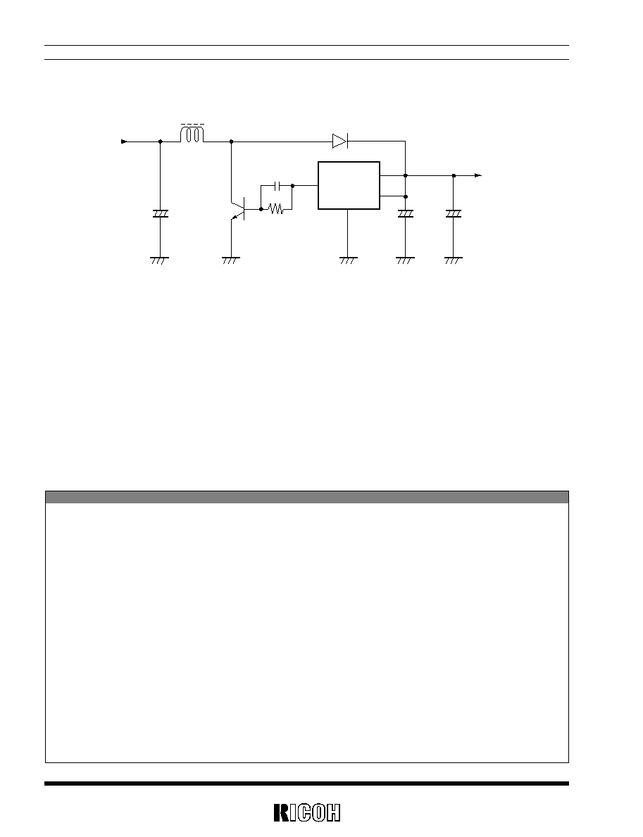
APPLICATION HINTS
L1
D1
V
OUT
CE
GND
V
OUT
V
IN
+
C2
+
C1
+
C3
Cb
Rb
Q1
EXT
RN5RYxx1
TYPICAL APPLICATIONS
Components : Inductor (L1)
: CD105
Diode (D1)
: D1FS4A (Schottky Type)
Capacitor (C1)
: 33ĶF (Tantalum Type)
Capacitor (C2)
: 47ĶF (Tantalum Type)
Capacitor (C3)
: 47ĶF (Tantalum Type)
Transistor (Q1)
: 2SD1628G
Base Resistor (Rb)
: 220
Base Capacitor (Cb)
: 2200pF
∑ A spike-shaped voltage higher than output voltage may be applied to the driver transistor. Therefore, care should be
paid regarding its absolute maximum ratings (V
DS
, V
CF
). We recommend to use a transistor having absolute maxi-
mum ratings of at least twice the set output voltage.
∑ We also recommend the use of an output capacitor with an allowable voltage which is at least 1.5 times the set out-
put voltage. This is because there may be the case where a spike-shaped voltage higher than the set output voltage
is generated.
Use capacitor with good high frequency characteristics such as tantalum capacitor.
∑ Choose such an inductor that a sufficiently small D.C. resistance and large allowable current, and hardly reaches
magnetic saturation.
∑ Use a diode of a Schottky type with high switching speed, and also take care of the rated current.
∑ Set external components as close as possible to the IC and minimize the current between the components and the
IC. In particular, make minimum connection with the output capacitor.
∑ Make sufficient grounding. A large current flows through GND pin by switching. When the impedance of the GND
connection is high, the potential within the IC is varied by the switching current. This may result in unstable opera-
tion of the IC.