 | –≠–ª–µ–∫—Ç—Ä–æ–Ω–Ω—ã–π –∫–æ–º–ø–æ–Ω–µ–Ω—Ç: RN5VD44C | –°–∫–∞—á–∞—Ç—å:  PDF PDF  ZIP ZIP |

VOLTAGE DETECTOR
WITH OUTPUT DELAY
RN5VD SERIES
1
OUTLINE
The RN5VD Series are CMOS-based voltage detector ICs with output delay functions and high detector
threshold accuracy and ultra-low supply current, which can be operated at an extremely low voltage and is
used,for instance, for system reset.
Each of these ICs consists of a voltage reference unit, a comparator, resistors for voltage detection, an
output driver, a hysteresis circuit and an output delay generator. The detector threshold is fixed with high
accuracy in the IC and requires no adjustment.
The RN5VD Series are operable by a lower voltage than that for the Rx5VL Series, and can be driven by
a single battery.
Two output types, Nch open drain type and CMOS type, are available. Since the package for these ICs
is SOT-23-5(Mini-mold)package, high density mounting of the ICs on board is possible.
∑ Output Delay ......................................................Typ. 100ms with external capacitor : 0.15µF
∑ Ultra-low Supply Current .................................Typ. 1.0µA (RN5VD15x : V
DD
=3.5V)
∑ Broad Operating Voltage Range.......................0.7V to 10.0V
∑ Detector Threshold ............................................Stepwise setting with a step of 0.1V in the range of 0.9V to 6.0V is
................................................................................
possible. (refer to Selection Guide) .
∑ High Accuracy Detector Threshold ..................±2.5%
∑ Low Temperature-Drift Coefficient of Detector Threshold ...........Typ. ±100ppm/∞C
∑ Two Output Types..............................................Nch Open Drain and CMOS
∑ Small Package ....................................................SOT-23-5(Mini-mold)
FEATURES
APPLICATIONS
∑
CPU & Logic Circuit Reset
∑
Battery Checker
∑
Window Comparator
∑
Wave Shaping Circuit
∑
Battery Back-Up Circuit
∑
Power Failure Detector
NO. EA-027-0301
RN5VDxxxx
≠
xx
Part Number
a bc d
SELECTION GUIDE
The detector threshold, the output type, the packing type, and the taping type of RN5VD Series can be desig-
nating at the user's request by specifying the part number as follows :
For example, the Product with Detector Threshold 3.5V, Output Type Nch Open Drain and Taping Type TR,
is designated by Part Number RN5VD35AA-TR.
Code
a
Setting Detector Threshold (≠V
DET
) :
Stepwise setting with a step of 0.1V in the range of 0.9V to 6.0V is possible.
b
Designation of Output Type
A: Nch Open Drain
C: CMOS
c
Designation of Packing Type
A: Taping
C: Antistatic bag for samples
d
Designation of Taping Type:
Ex. SOT-23-5: TR, TL
(refer to Taping Specification)
"TR" is prescribed as a standard.
Contents
RN5VD
2
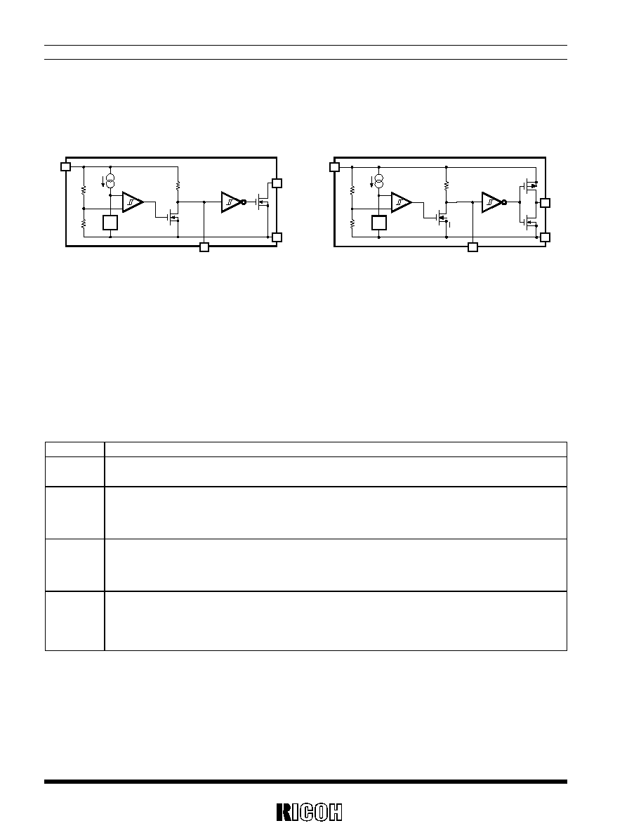
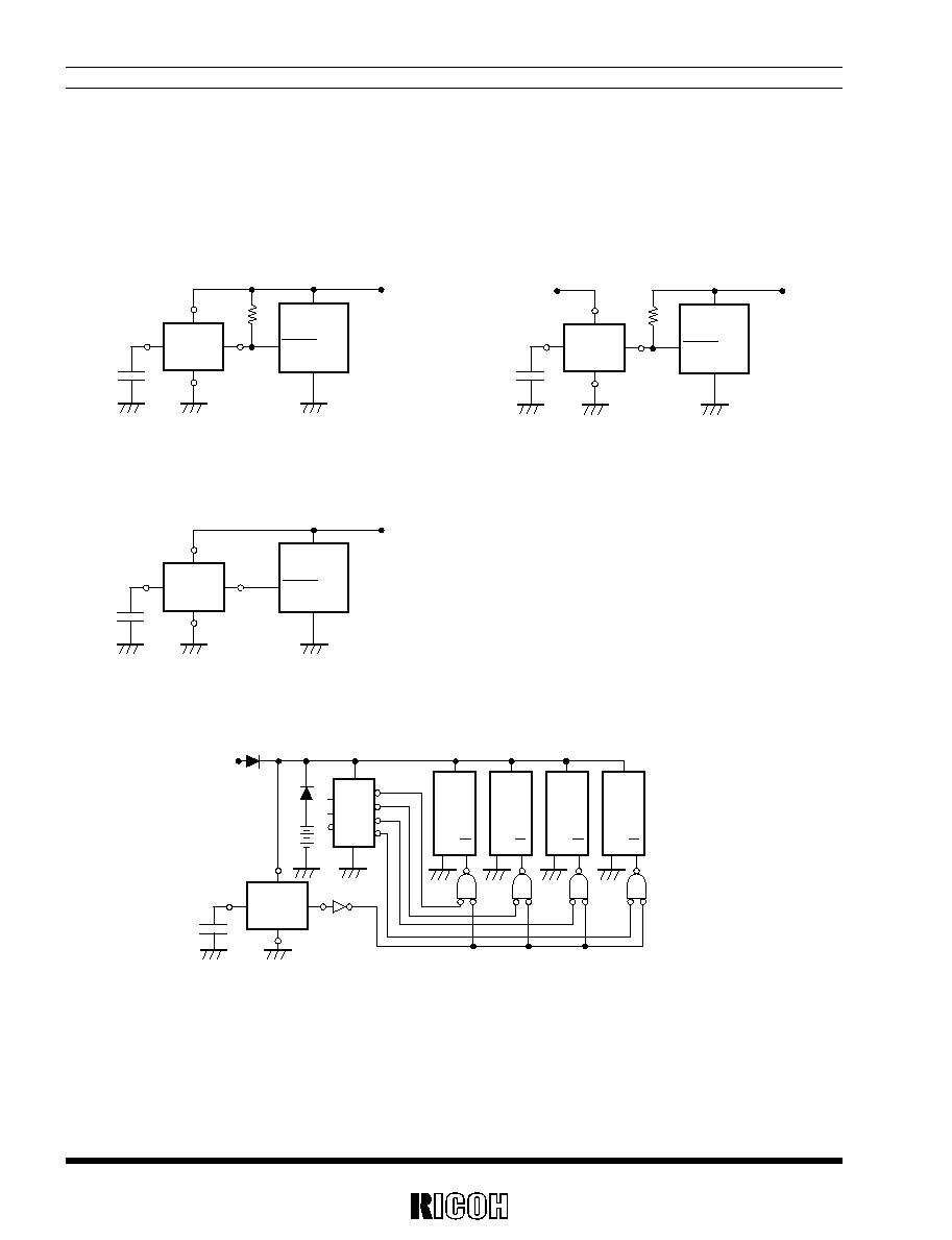
BLOCK DIAGRAMS
2
3
Vref
OUT
GND
V
DD
C
D
R
D
≠
+
1
5
2
3
Vref
OUT
GND
V
DD
C
D
R
D
≠
+
1
5
∑
Nch Open Drain Output (RN5VDxxA)
∑
CMOS Output (RN5VDxxC)
}
}
RN5VD
3
ABSOLUTE MAXIMUM RATINGS
Symbol
Item
Rating
Unit
V
DD
Supply Voltage
12
V
OUT
Output Voltage
I
OUT
Output Current
Power Dissipation
CNOS
V
SS
≠0.3 to V
DD
+0.3
Nch
70
P
D
150
V
SS
≠0.3 to 12
V
V
mA
mW
Operating Temperature Range
Topt
≠40 to +85
∞C
Storage Temperature Range
Tstg
≠55 to +125
∞C
Lead Temperature (Soldering)
Tsolder
260∞C, 10s
Absolute Maximum ratings are threshold limit values that must not be exceeded even for an instant under any
conditions. Moreover, such values for any two items must not be reached simultaneously. Operation above
these absolute maximum ratings may cause degradation or permanent damage to the device. These are stress
ratings only and do not necessarily imply functional operation below these limits.
ABSOLUTE MAXIMUM RATINGS
PIN DESCRIPTION
Pin No.
Symbol
Description
1
OUT
Output Pin
Input and power source for device itself
Ground Pin
No Connection
Pin for external capacitor (for setting output delay)
2
V
DD
3
GND
4
NC
5
C
D
PIN CONFIGURATION
∑ SOT-23-5
1
2
3
5
4
(mark side)
RN5VD
4
V
DD
=0.8V
V
DD
=2.9V
≠V
DET
Topt
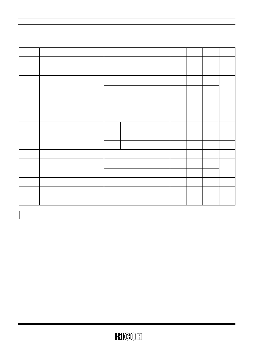
ELECTRICAL CHARACTERISTICS
∑ RN5VD09A/C
Topt=25∞C
Symbol
Item
Conditions
Min.
Typ.
Max.
Unit.
≠V
DET
V
HYS
I
SS
Detector Threshold
Detector Threshold Hysteresis
Supply Current
0.878
0.900
0.922
V
0.027
0.045
0.063
V
1.5
0.9
3.7
2.7
µA
V
DDH
Maximum Operating Voltage
10
V
V
DDL
Minimum Operating Voltage
(
Note
1)
Topt=25∞C
≠30∞C
Topt85∞C
0.55
0.65
0.70
0.80
V
I
OUT
Output Current
Nch
Pch
V
DS
=0.05V, V
DD
=0.7V
V
DS
=0.5V, V
DD
=0.85V
V
DS
=≠2.1V, V
DD
=4.5V
0.01
0.05
1.0
0.05
0.50
2.0
mA
V
TCD
C
D
pin Threshold Voltage
V
DD
=0.99V
0.297
0.495
0.693
V
mA
R
D
Delay Resistance
0.5
1.0
2.0
M
Detector Threshold
Temperature Coefficient
≠30∞C
Topt85∞C
±100
ppm/∞C
I
CD
C
D
pin Sink Current
V
DS
=0.1V, V
DD
=0.7V
V
DS
=0.5V, V
DD
=0.85V
2.0
10.0
30
100.0
µA
(Note 1) Minimum Operating Voltage means the value of input voltage when output voltage maintains 0.1V or less, provided that in the case of Nch
Open Drain Type Products, the pull-up resistance is set at 470k
, and the pull-up voltage is set at 5.0V.
RN5VD
5
∑ RN5VD18A/C
Topt=25∞C
Symbol
Item
Conditions
Min.
Typ.
Max.
Unit.
≠V
DET
V
HYS
I
SS
V
DDH
Detector Threshold
Detector Threshold Hysteresis
Supply Current
Maximum Operating Voltage
V
DD
=1.7V
V
DD
=3.8V
1.755
1.800
1.845
V
0.054
0.090
0.126
V
2.5
1.0
5.0
3.0
µA
10
V
V
DDL
Minimum Operating Voltage
(
Note
1)
Topt=25∞C
≠30∞C
Topt85∞C
0.55
0.65
0.70
0.80
V
I
OUT
Output Current
Nch
Pch
V
DS
=≠2.1V, V
DD
=4.5V
V
DS
=0.05V, V
DD
=0.7V
V
DS
=0.5V, V
DD
=1.5V
0.01
1.0
0.05
2.0
1.0
2.0
mA
mA
V
TCD
C
D
pin Threshold Voltage
V
DD
=1.98V
0.693
0.990
1.287
V
I
CD
C
D
pin Sink Current
V
DS
=0.1V, V
DD
=0.7V
V
DS
=0.5V, V
DD
=1.5V
2.0
200.0
30
800.0
µA
R
D
Delay Resistance
0.5
1.0
2.0
M
≠V
DET
Topt
Detector Threshold
Temperature Coefficient
≠30∞C
Topt85∞C
±100
ppm/∞C
(Note 1) Minimum Operating Voltage means the value of input voltage when output voltage maintains 0.1V or less, provided that in the case of Nch
Open Drain Type Products, the pull-up resistance is set at 470k
, and the pull-up voltage is set at 5.0V.
RN5VD
6
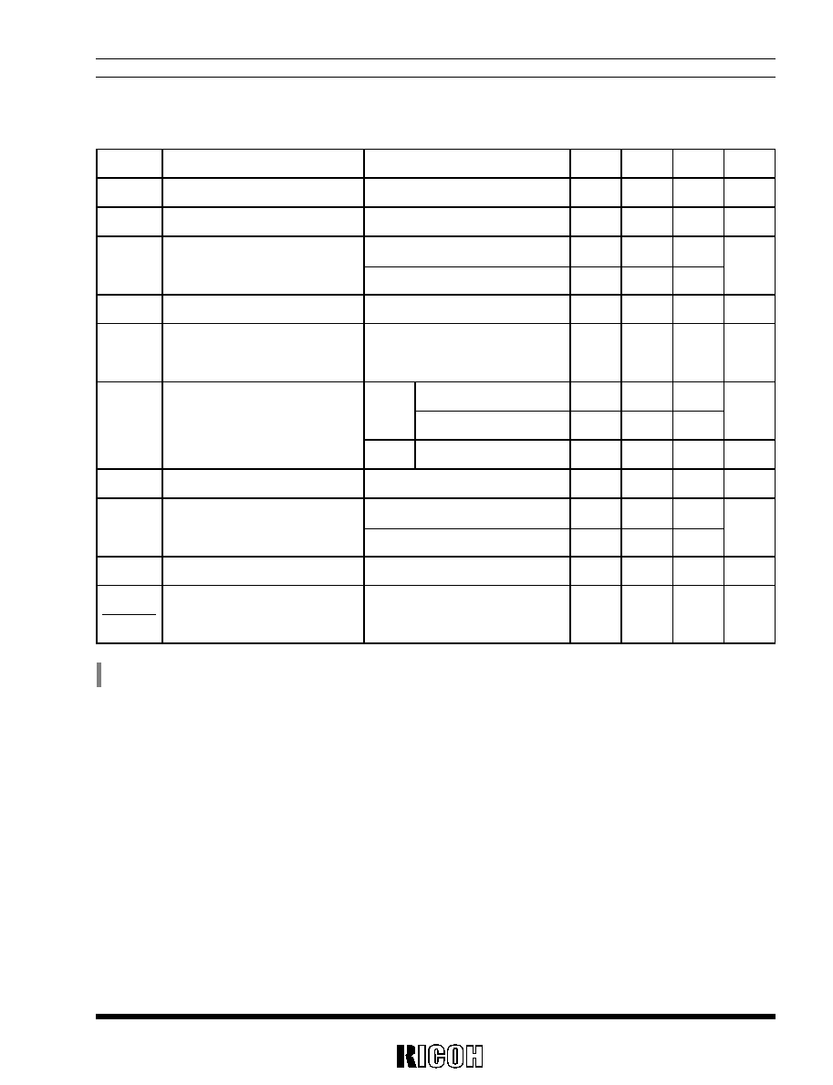
∑ RN5VD27A/C
Topt=25∞C
Symbol
Item
Conditions
Min.
Typ.
Max.
Unit.
≠V
DET
V
HYS
I
SS
V
DDH
Detector Threshold
Detector Threshold Hysteresis
Supply Current
Maximum Operating Voltage
V
DD
=2.6V
V
DD
=4.7V
2.633
2.700
2.767
V
0.081
0.135
0.189
V
3.5
1.1
7.0
3.3
µA
10
V
V
DDL
Minimum Operating Voltage
(
Note
1)
Topt=25∞C
≠30∞C
Topt85∞C
0.55
0.65
0.70
0.80
V
I
OUT
Output Current
Nch
Pch
V
DS
=≠2.1V, V
DD
=4.5V
V
DS
=0.05V, V
DD
=0.7V
V
DS
=0.5V, V
DD
=1.5V
0.01
1.0
0.05
2.0
1.0
2.0
mA
mA
V
TCD
C
D
pin Threshold Voltage
V
DD
=2.97V
1.188
1.485
1.782
V
I
CD
C
D
pin Sink Current
V
DS
=0.1V, V
DD
=0.7V
V
DS
=0.5V, V
DD
=1.5V
2.0
200.0
30
800.0
µA
R
D
Delay Resistance
0.5
1.0
2.0
M
≠V
DET
Topt
Detector Threshold
Temperature Coefficient
≠30∞C
Topt85∞C
±100
ppm/∞C
( Note 1) Minimum Operating Voltage means the value of input voltage when output voltage maintains 0.1V or less, provided that in the case of Nch
Open Drain Type Products, the pull-up resistance is set at 470k
, and the pull-up voltage is set at 5.0V.
RN5VD
7
∑ RN5VD36A/C
Topt=25∞C
Symbol
Item
Conditions
Min.
Typ.
Max.
Unit.
≠V
DET
V
HYS
Detector Threshold
Detector Threshold Hysteresis
3.510
3.600
3.690
V
0.108
0.180
0.252
V
I
SS
Supply Current
V
DD
=3.47V
V
DD
=5.6V
4.5
1.2
9.0
3.6
µA
V
DDH
Maximum Operating Voltage
10
V
V
DDL
Minimum Operating Voltage
(
Note
1)
Topt=25∞C
≠30∞C
Topt85∞C
0.55
0.65
0.70
0.80
V
I
OUT
Output Current
Nch
Pch
V
DS
=0.05V, V
DD
=0.7V
V
DS
=0.5V, V
DD
=1.5V
V
DS
=≠2.1V, V
DD
=4.5V
0.01
1.0
2.0
1.0
2.0
0.05
mA
mA
V
TCD
C
D
pin Threshold Voltage
V
DD
=3.96V
1.584
1.980
2.376
V
I
CD
C
D
pin Sink Current
V
DS
=0.1V, V
DD
=0.7V
V
DS
=0.5V, V
DD
=1.5V
2.0
200.0
30
800.0
µA
R
D
Delay Resistance
0.5
1.0
2.0
M
≠V
DET
Topt
Detector Threshold
Temperature Coefficient
≠30∞C
Topt85∞C
±100
ppm/∞C
(Note 1) Minimum Operating Voltage means the value of input voltage when output voltage maintains 0.1V or less, provided that in the case of Nch
Open Drain Type Products, the pull-up resistance is set at 470k
, and the pull-up voltage is set at 5.0V.

RN5VD
8
∑ RN5VD45A/C
Topt=25∞C
Symbol
Item
Conditions
Min.
Typ.
Max.
Unit.
≠V
DET
V
HYS
Detector Threshold
Detector Threshold Hysteresis
4.388
4.500
4.612
V
0.135
0.225
0.315
V
I
SS
Supply Current
V
DD
=4.34V
V
DD
=6.5V
5.5
1.3
11.0
3.9
µA
V
DDL
Minimum Operating Voltage
(
Note
1)
Topt=25∞C
≠30∞C
Topt85∞C
0.55
0.65
0.70
0.80
V
I
OUT
Output Current
V
TCD
C
D
pin Threshold Voltage
Nch
V
DS
=0.05V, V
DD
=0.7V
V
DS
=0.5V, V
DD
=1.5V
V
DS
=≠2.1V, V
DD
=8.0V
Pch
0.01
1.0
0.05
2.0
1.5
3.0
V
DD
=4.95V
1.980
2.475
2.970
V
I
CD
C
D
pin Sink Current
V
DS
=0.1V, V
DD
=0.7V
V
DS
=0.5V, V
DD
=1.5V
2.0
200.0
30
800.0
µA
R
D
Delay Resistance
0.5
1.0
2.0
M
≠V
DET
Topt
Detector Threshold
Temperature Coefficient
≠30∞C
Topt85∞C
±100
ppm/∞C
mA
mA
V
DDH
Maximum Operating Voltage
10
V
(Note 1) Minimum Operating Voltage means the value of input voltage when output voltage maintains 0.1V or less, provided that in the case of Nch
Open Drain Type Products, the pull-up resistance is set at 470k
, and the pull-up voltage is set at 5.0V.

RN5VD
9
∑ RN5VD54A/C
Topt=25∞C
Symbol
Item
Conditions
Min.
Typ.
Max.
Unit.
≠V
DET
Detector Threshold
5.265
5.400
5.535
0.378
V
V
HYS
Detector Threshold Hysteresis
0.162
0.270
V
12.0
4.2
I
SS
Supply Current
V
DD
=5.2V
V
DD
=7.4V
6.0
1.4
µA
10
V
DDH
Maximum Operating Voltage
V
0.70
0.80
V
DDL
Minimum Operating Voltage
(
Note
1)
Topt=25∞C
≠30∞C
Topt85∞C
0.55
0.65
V
0.05
2.0
3.564
V
TCD
C
D
pin Threshold Voltage
V
DD
=5.94V
2.376
2.970
V
2.0
R
D
Delay Resistance
0.5
1.0
M
≠V
DET
Topt
Detector Threshold
Temperature Coefficient
≠30∞C
Topt85∞C
±100
ppm/∞C
I
CD
C
D
pin Sink Current
V
DS
=0.1V, V
DD
=0.7V
V
DS
=0.5V, V
DD
=1.5V
2.0
200.0
30
800.0
µA
I
OUT
Output Current
Nch
V
DS
=0.05V, V
DD
=0.7V
V
DS
=0.5V, V
DD
=1.5V
0.01
1.0
mA
mA
3.0
Pch
V
DS
=≠2.1V, V
DD
=8.0V
1.5
(Note 1) Minimum Operating Voltage means the value of input voltage when output voltage maintains 0.1V or less, provided that in the case of Nch
Open Drain Type Products, the pull-up resistance is set at 470k
, and the pull-up voltage is set at 5.0V.
RN5VD
10
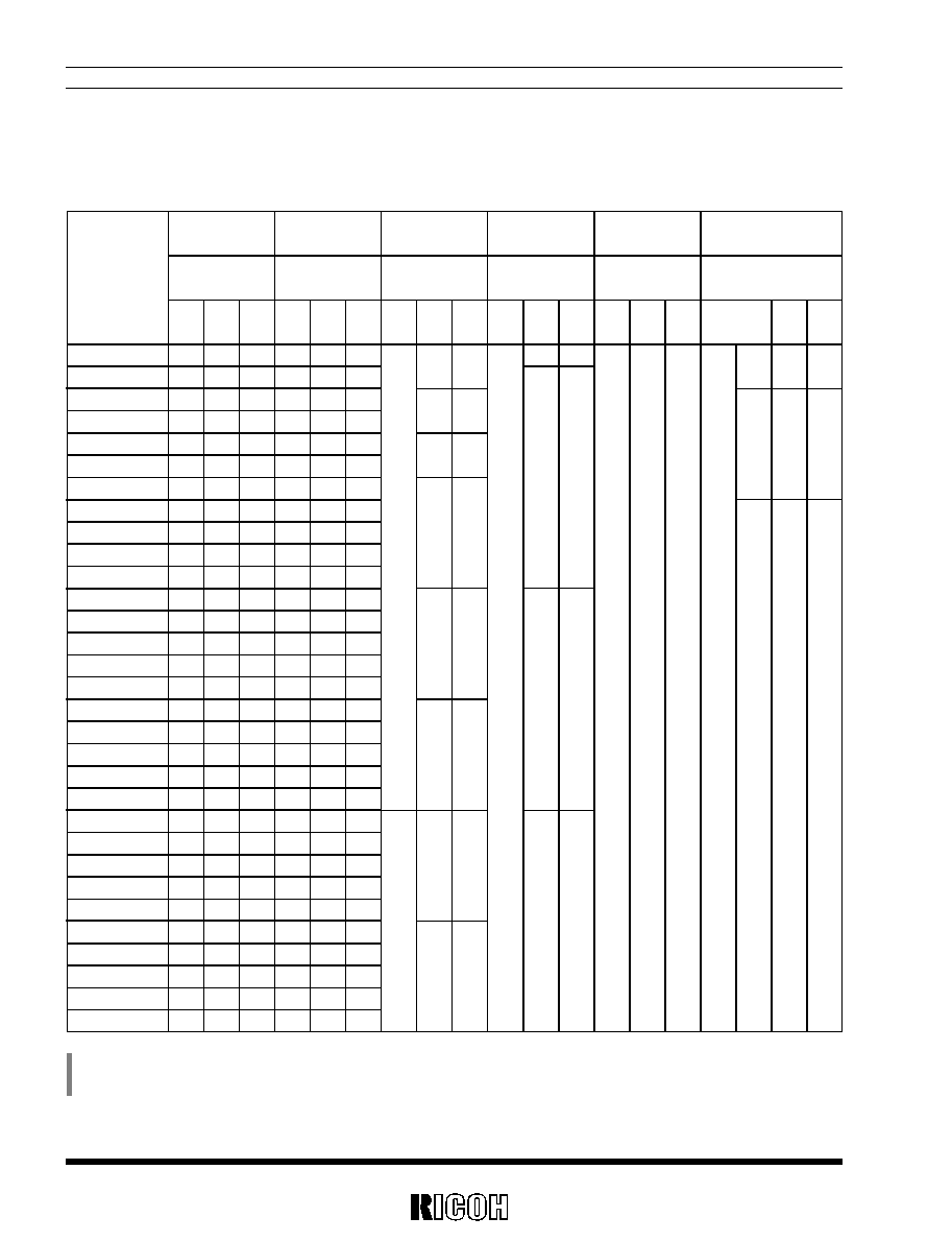
Part Number.
RN5VD09A/C
RN5VD10A/C
RN5VD11A/C
RN5VD12A/C
RN5VD13A/C
RN5VD14A/C
RN5VD15A/C
RN5VD16A/C
RN5VD17A/C
RN5VD18A/C
RN5VD19A/C
RN5VD20A/C
RN5VD21A/C
RN5VD22A/C
RN5VD23A/C
RN5VD24A/C
RN5VD25A/C
RN5VD26A/C
RN5VD27A/C
RN5VD28A/C
RN5VD29A/C
RN5VD30A/C
RN5VD31A/C
RN5VD32A/C
RN5VD33A/C
RN5VD34A/C
RN5VD35A/C
RN5VD36A/C
RN5VD37A/C
RN5VD38A/C
RN5VD39A/C
Detector Threshold
≠V
DET
(V)
Min
.
Typ. Max.
0.878 0.900 0.922 0.027 0.045 0.063
0.975 1.000 1.025 0.030 0.050 0.070
1.073 1.100 1.127 0.033 0.055 0.077
1.170 1.200 1.230 0.036 0.060 0.084
1.268 1.300 1.332 0.039 0.065 0.091
1.365 1.400 1.435 0.042 0.070 0.098
1.463 1.500 1.537 0.045 0.075 0.105
1.560 1.600 1.640 0.048 0.080 0.112
1.658 1.700 1.742 0.051 0.085 0.119
1.755 1.800 1.845 0.054 0.090 0.126
1.853 1.900 1.947 0.057 0.095 0.133
1.950 2.000 2.050 0.060 0.100 0.140
2.048 2.100 2.152 0.063 0.105 0.147
2.145 2.200 2.255 0.066 0.110 0.154
2.243 2.300 2.357 0.069 0.115 0.161
2.340 2.400 2.460 0.072 0.120 0.168
2.438 2.500 2.562 0.075 0.125 0.175
2.535 2.600 2.665 0.078 0.130 0.182
2.633 2.700 2.767 0.081 0.135 0.189
2.730 2.800 2.870 0.084 0.140 0.196
2.828 2.900 2.972 0.087 0.145 0.203
2.925 3.000 3.075 0.090 0.150 0.210
3.023 3.100 3.177 0.093 0.155 0.217
3.120 3.200 3.280 0.096 0.160 0.224
3.218 3.300 3.382 0.099 0.165 0.231
3.315 3.400 3.485 0.102 0.170 0.238
3.413 3.500 3.587 0.105 0.175 0.245
3.510 3.600 3.690 0.108 0.180 0.252
3.608 3.700 3.792 0.111 0.185 0.259
3.705 3.800 3.895 0.114 0.190 0.266
3.803 3.900 3.997 0.117 0.195 0.273
V
DD
=
(≠V
DET
)
≠0.10V
V
DD
=
(≠V
DET
)
≠0.13V
1.5
1.8
3.7
4.5
2.0
5.0
2.5
5.0
3.0
6.0
3.5
7.0
4.0
8.0
4.5
9.0
V
DD
=
(≠V
DET
)
+2.0V
0.9
2.7
1.0
3.0
1.1
3.3
1.2
3.6
Nch
V
DS
=
0.05V
V
DD
=
0.7V
0.01 0.05
Nch
V
DS
=
0.5V
V
DD
=
0.85V
0.05 0.50
V
DD
=
1.0V
0.2
1.0
V
DD
=
1.5V
1.0
2.0
Min
.
Typ. Max.
condi-
tions
Typ. Max.
condi-
tions
Typ. Max.
condi-
tions
Min. Typ.
conditions
Min. Typ.
V
HYS
(V)
Iss
1
(µA)
Iss
2
(µA)
I
OUT
1
(mA)
I
OUT
2
(mA)
Hysteresis
Supply Current 1 Supply Current 2 Output Current 1
Output Current 2
ELECTRICAL CHARACTERISTICS BY DETECTOR THRESHOLD
∑ RN5VD09A/C to RN5VD39A/C
(Note) Refer to the previously defined "Minimum Operating Voltage".
Condition 1 : Topt=25∞C
Condition 2 : ≠30∞C
Topt85∞C
RN5VD
11
P
ch
V
DS
=
≠2.1V
V
DD
=
4.5V
1.0
2.0
(Note1)
Condition1
0.55
Condition2
0.65
(Note1)
Condition1
0.70
Condition2
0.80
V
DD
=
(≠V
DET
)
◊
1.1V
V
DS
=
0.1V
V
DD
=
0.7V
2.0
30
V
DS
=
0.5V
V
DD
=
0.85V
V
DD
=
1.0V
V
DD
=
1.5V
10
50
200
100
200
800
0.5
1.0
2.0
Output Current 3
I
OUT
3 (
mA)
condi-
tions
Min. Typ.
Typ.
Max.
condi-
tions
V
DD
◊
0.3
V
DD
◊
0.35
V
DD
◊
0.4
V
DD
◊
0.5
V
DD
◊
0.5
V
DD
◊
0.5
V
DD
◊
0.7
V
DD
◊
0.65
V
DD
◊
0.6
Min. Typ. Max.
condi-
tions
Min. Typ.
conditions
Min. Typ. Min. Typ. Max.
V
DDL
(V)
V
TCD
(V)
I
CD
1
(µA)
I
CD
2
(µA)
R
D
(M
)
Minimum Oper-
ating Voltage
C
D
Pin Threshold Voltage
C
D
Pin Output
Current 1
C
D
Pin Output Current 2
Delay
Resistance
≠30∞C
Topt
85∞C ±100
condi-
tions
Typ.
≠V
DET
Topt (ppm/∞C)
Detector
Threshold
Tempco.
Topt=25∞C
RN5VD
12
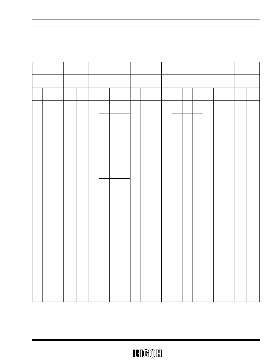
Part Number.
RN5VD40A/C
RN5VD41A/C
RN5VD42A/C
RN5VD43A/C
RN5VD44A/C
RN5VD45A/C
RN5VD46A/C
RN5VD47A/C
RN5VD48A/C
RN5VD49A/C
RN5VD50A/C
RN5VD51A/C
RN5VD52A/C
RN5VD53A/C
RN5VD54A/C
RN5VD55A/C
RN5VD56A/C
RN5VD57A/C
RN5VD58A/C
RN5VD59A/C
RN5VD60A/C
Detector Threshold
≠V
DET
(V)
Min. Typ. Max. Min. Typ. Max.
condi-
tions
Typ. Max.
condi-
tions
Typ. Max.
condi-
tions
Min. Typ.
Min. Typ.
3.900 4.000 4.100 0.120 0.200 0.280
3.998 4.100 4.202 0.123 0.205 0.287
4.095 4.200 4.305 0.126 0.210 0.294
4.193 4.300 4.407 0.129 0.215 0.301
4.290 4.400 4.510 0.132 0.220 0.308
4.388 4.500 4.612 0.135 0.225 0.315
4.485 4.600 4.715 0.138 0.230 0.322
4.583 4.700 4.817 0.141 0.235 0.329
4.680 4.800 4.920 0.144 0.240 0.336
4.778 4.900 5.022 0.147 0.245 0.343
4.875 5.000 5.125 0.150 0.250 0.350
4.973 5.100 5.227 0.153 0.255 0.357
5.070 5.200 5.330 0.156 0.260 0.364
5.168 5.300 5.432 0.159 0.265 0.371
5.265 5.400 5.535 0.162 0.270 0.378
5.363 5.500 5.637 0.165 0.275 0.385
5.460 5.600 5.740 0.168 0.280 0.392
5.558 5.700 5.842 0.171 0.285 0.399
5.655 5.800 5.945 0.174 0.290 0.406
5.753 5.900 6.047 0.177 0.295 0.413
5.850 6.000 6.150 0.180 0.300 0.420
V
DD
=
(≠V
DET
)
≠0.16V
V
DD
=
(≠V
DET
)
≠0.20V
5.0
10.0
5.5
11.0
6.0
12.0
6.5
13.0
V
DD
=
(≠V
DET
)
+2.0V
1.3
3.9
1.4
4.2
N
ch
V
DS
=
0.05V
V
DD
=
0.7V
0.01 0.05
N
ch
V
DS
=
0.5V
V
DD
=
1.5V
1.0
2.0
conditions
V
HYS
(V)
Iss
1
(µA)
Iss
2
(µA)
I
OUT
1
(mA)
I
OUT
2
(mA)
Hysteresis
Supply Current 1 Supply Current 2 Output Current 1
Output Current 2
∑ RN5VD40A/C to RN5VD60A/C
(Note) Refer to the previously defined "Minimum Operating Voltage".
Condition 1 : Topt=25∞C
Condition 2 : ≠30∞C
Topt85∞C
RN5VD
13
P
ch
V
DS
=
≠2.1V
V
DD
=
8.0V
1.5
3.0
(Note1)
Condition1
0.55
Condition2
0.65
(Note1)
Condition1
0.70
Condition2
0.80
V
DD
=
(≠
V
DET
)
◊
1.1V
V
DS
=
0.1V
V
DD
=
0.7V
2.0
30
V
DS
=
0.5V
V
DD
=
1.5V
200
800
0.5
1.0
2.0
Output Current 3
I
OUT
3
(mA)
condi-
tions
Min. Typ.
Typ.
Max.
condi-
tions
V
DD
◊
0.4
V
DD
◊
0.5
V
DD
◊
0.6V
Min. Typ. Max.
condi-
tions
Min. Typ.
conditions
Min. Typ.
condi-
tions
Typ. Max.
V
DDL
(V)
V
TCD
(V)
I
CD
1
(µA)
I
OUT
1
(mA)
I
OUT
2
(mA)
Minimum Oper-
ating Voltage
C
D
Pin Threshold Voltage
C
D
Pin Output
Current 1
C
D
Pin Output Current 2
Delay
Resistance
≠30∞C
Topt
85∞C ±100
condi-
tions
Typ.
Detector
Threshold
Tempco.
Topt=25∞C
≠V
DET
Topt (ppm/∞C)
RN5VD
14
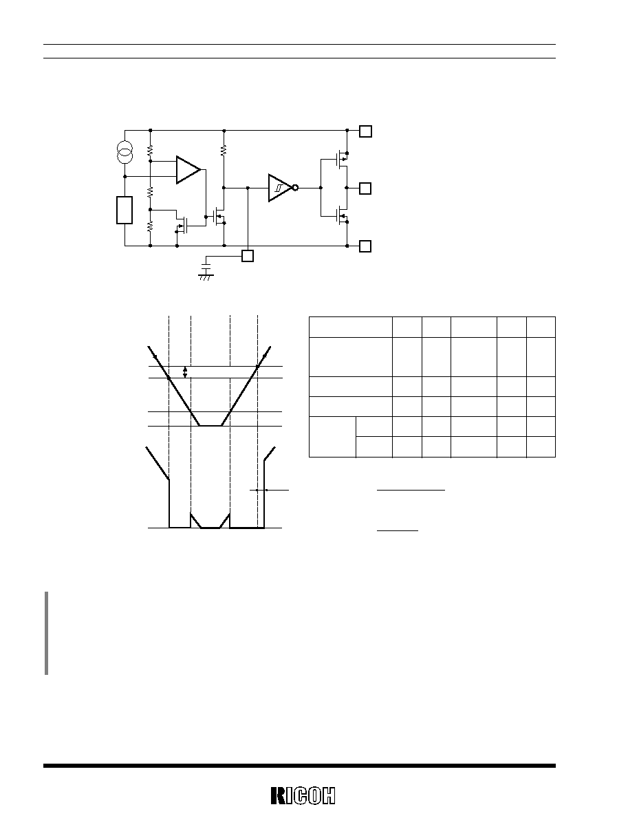
A
B
1 2 3 4 5
Detector Threshold Hysteresis
Released Voltage +V
DET
Detected Voltage ≠V
DET
Minimum Operaing Voltage
Delay Time
GND
GND
Supply Voltage
(V
DD
)
Output Voltage
(OUT)
OPERATION
Fig. 2 Operation Diagram
Fig. 1 Block Diagram
Step 1. Output voltage is equal to pull-up voltage.
Step 2. When input voltage (V
DD
) reaches the state of Vref
V
DD
∑ (Rb+Rc) / (Ra+Rb+Rc) at point A (Detected Voltage ≠V
DET
) , the output of comparator is
reversed, so that output voltage becomes GND. Discharging is performed from C
D
pin connected to an external capacitor. No delay time is generated.
Step 3.
Output voltage becomes indefinite when power source voltage(V
DD
) is smaller than minimum operating voltage. When the output is pulled up, V
DD
is
output.
Step 4. Output voltage becomes equal to GND.
Step 5. When input voltage (V
DD
) reaches the state of Vref
V
DD
∑ Rb/ (Ra+Rb) at Point B (Released Voltage +V
DET
) , the output of comparator is reversed,
and the external capacitor is charged through C
D
pin, so that output voltage becomes equal to pulled-up voltage after a delay time
t
D
(=0.69
◊
10
6
◊
C
D
) .
Step
Step 1
Step 2
Step 3
Step 4
Step 5
Comparator (≠) Pin
Input Voltage
I
II
II
II
I
Comparator Output
L
H
Indefinite
H
L
Tr. 1, 2
OFF
ON
Indefinite
ON
OFF
Output Tr.
Nch
OFF
ON
Indefinite
ON
OFF
Pch
ON
OFF
Indefinite
OFF
ON
I.
Rb + Rc
Ra + Rb + Rc
∑ V
DD
II.
Rb
Ra + Rb
∑ V
DD
GND
OUT
C
D
V
DD
Ra
Current Source
Output Capacitor
R
D
Rb
Rc
Tr.1
Tr.2
Vref
≠
+
Comparator
Schmitt Trigger
Nch
Pch
RN5VD
15
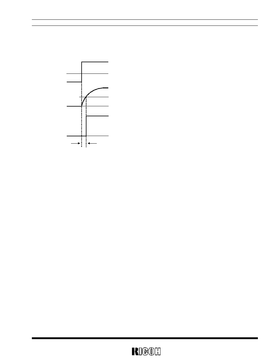
∑ Output Delay Operation
When the supply voltage crosses the released voltage (+V
DET
) from a low value to a value higher than
the released voltage (+V
DET
) , the C
D
pin voltage starts to increase (starts to charge the external capaci-
tor).
The output voltage is maintained at "L" level until the C
D
pin voltage reaches to V
TCD
(C
D
pin threshold
voltage) after that the output voltage is reversed to "H".
The time period from beginning of charging capacitor to output voltage reversing represents the out-
put delay (
t
D
) .
Supply Voltage
(V
DD
)
C
D
pin Voltage
Output Voltage
(OUT)
Output Delay Time (
t
D
)
GND
C
D
pin Threshold Voltage (V
TCD
)
Released Voltage (+V
DET
)
GND
Delay time (
t
D
) can be set accordance with the capacitance C
D
of external capacitor as below
t
D
=0.69
◊
10
6
◊
C
D
(s)
∑ Output Delay Time

RN5VD
16
TEST CIRCUITS
Fig. 3 Supply Current test Circuit
Fig. 4 Detector Threshold Test Circuit
Fig. 5 Nch Driver Output Current Test Circuit
Fig. 6 Pch Driver Output Current Test Circuit
Fig. 7 C
D
pin Threshold Voltage Test Circuit
Fig. 8 C
D
pin Sink Current Test Circuit
Fig. 9 Output Delay Time Test Circuit
V
IN
I
SS
V
DD
GND
RN5VD
SERIES
V
IN
V
DD
+5V or V
DD
GND
OUT
470k
RN5VD
SERIES
V
IN
V
DD
GND
OUT
RN5VD
SERIES
V
DS
I
OUT
V
IN
V
DD
GND
OUT
RN5VD
◊◊
C
SERIES
V
DD+
V
DS
I
OUT
V
IN
V
DD
C
D
V
DS
+5V or V
DD
GND
OUT
OUT
470k
RN5VD
SERIES
V
IN
V
DD
C
D
V
DS
GND
RN5VD
SERIES
I
CD
t
PHL
t
D
+V
DET
+2.0V
100%
50%
GND
0.7V
GND
Input Voltage
Output Voltage
C
D
C
D
V
DD
+5V
GND
OUT
470k
RN5VD
SERIES
V
IN
*
) at Fig.4,7,9. CMOS Output Type does not
need a pull-up resistor.
RN5VD
17
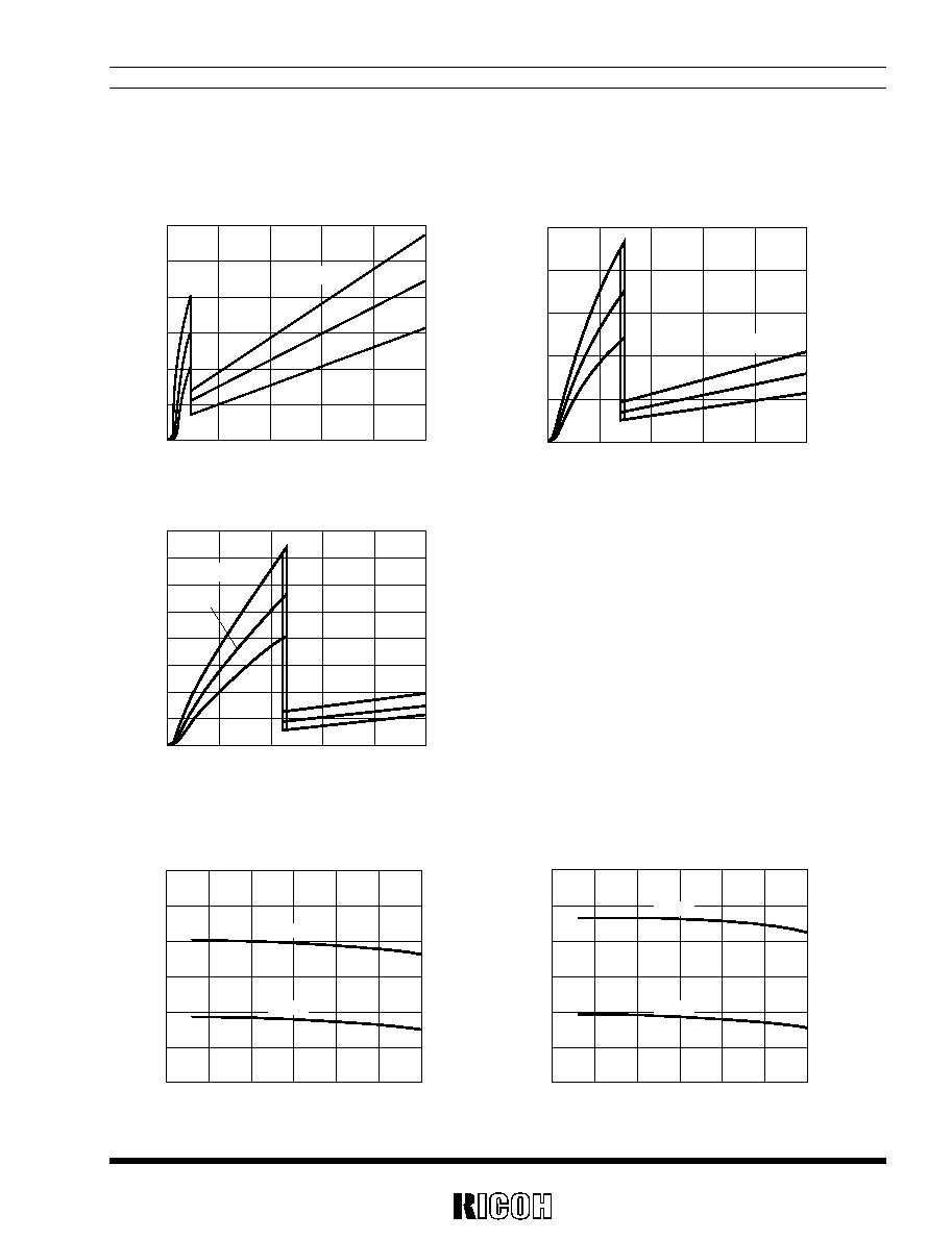
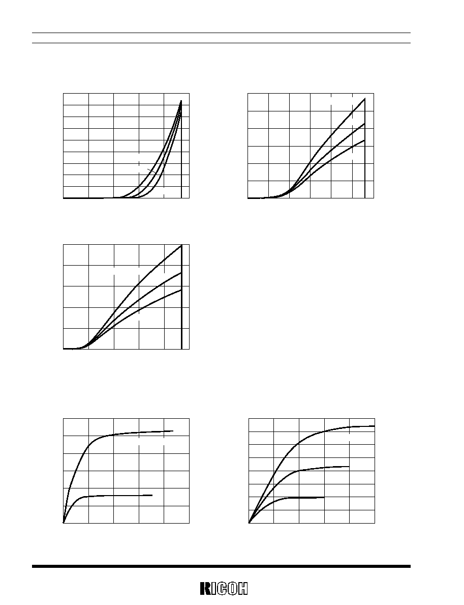
TYPICAL CHARACTERISTICS
1) Supply Current vs. Input Voltage
0
2
4
6
8
10
0
0.5
1.0
1.5
2.0
2.5
3.0
Supply Current Iss(
µ
A)
RN5VD09x
Input Voltage V
IN
(V)
Topt=80∞C
25∞C
≠30∞C
0
1
2
3
4
5
0
2
4
6
8
10
Supply Current Iss(
µ
A)
Input Voltage V
IN
(V)
RN5VD27x
Topt=80∞C
25∞C
≠30∞C
0
3
4
5
6
7
8
Supply Current Iss(
µ
A)
0
2
4
6
8
10
Input Voltage V
IN
(V)
RN5VD45x
Topt=80∞C
25∞C
≠30∞C
2
1
2) Detector Threshold vs. Temperature
≠40
≠20
0
20
40
60
80
0.86
0.88
0.90
0.92
0.94
0.96
0.98
Detector Threshold V
DET
(
V
)
RN5VD09x
Temperature Topt(∞C)
+V
DET
≠V
DET
2.60
2.65
2.70
2.75
2.80
2.85
2.90
Detector Threshold V
DET
(V)
RN5VD27x
≠40
≠20
0
20
40
60
80
Temperature Topt(∞C)
≠V
DET
+V
DET
RN5VD
18
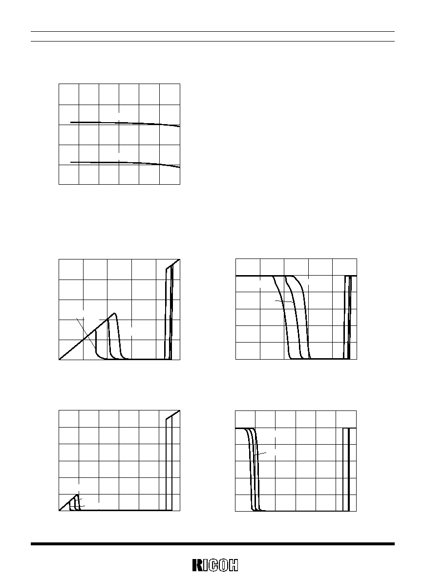
3) Output Voltage vs. Input Voltage
0
0.2
0.4
0.6
0.8
1
0
0.2
0.4
0.6
0.8
1.0
Output Voltage V
OUT
(V)
RN5VD09A
Input Voltage V
IN
(V)
25∞C
≠30∞C
Topt
=
80∞C
V
DD
Pull-up
470k
0
0.2
0.4
0.6
0.8
1.0
0
1
2
3
4
5
6
Output Voltage V
OUT
(V)
RN5VD09A
Input Voltage V
IN
(V)
Topt
=
80∞C
25∞C
≠30∞C
5V Pull-up
470k
0
0.5
1.0
1.5
2.0
2.5
3.0
0
0.5
1.0
1.5
2.0
2.5
3.0
Output Voltage V
OUT
(V)
RN5VD27A
Input Voltage V
IN
(V)
Topt
=
≠30∞C
25∞C
80∞C
V
DD
Pull-up
470k
0
0.5
1.0
1.5
2.0
2.5
3.0
0
1
2
3
4
5
6
Output Voltage V
OUT
(V)
RN5VD27A
Input Voltage V
IN
(V)
25∞C
Topt
=
≠30∞C
80∞C
5V Pull-up
470k
≠40
≠20
0
20
40
60
80
4.4
4.5
4.6
4.7
4.8
4.9
Detector Threshold V
DET
(V)
RN5VD45x
Temperature Topt(∞C)
+V
DET
≠V
DET
RN5VD
19
0
1
2
3
4
5
0
1
2
3
4
5
Output Voltage V
OUT
(V)
RN5VD45A
Input Voltage V
IN
(V)
Topt
=
≠30∞C
25∞C
80∞C
V
DD
Pull-up
470k
0
1
2
3
4
6
5
Output Voltage V
OUT
(V)
RN5VD45A
0
1
2
3
4
5
Input Voltage V
IN
(V)
Topt
=
≠30∞C
25∞C
80∞C
5V Pull-up
470k
4) Nch Driver Output Current vs. V
DS
0
0.2
0.4
0.6
0.8
1.0
0
0.05
0.10
0.15
0.20
0.25
0.30
0.35
0.40
0.45
Output Currert I
OUT
(mA)
RN5VD09x
V
DS
(V)
V
DD=
0.85V
0.7V
0
5
10
15
20
25
30
35
40
Output Currert I
OUT
(mA)
0
1
2
3
4
RN5VD45x
V
DS
(V)
1.5V
2.0V
2.5V
3.0V
3.5V
V
DD
=4.0V
RN5VD27x
0
0.5
1.0
1.5
2.0
2.5
V
DS
(V)
0
2
4
6
8
10
12
14
16
Output Currert I
OUT
(mA)
V
DD=
2.5V
2.0V
1.5V
RN5VD
20
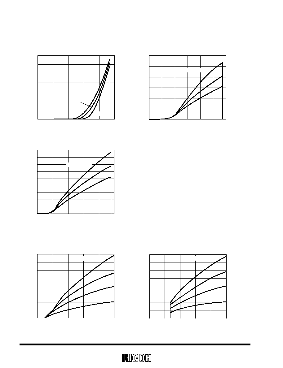
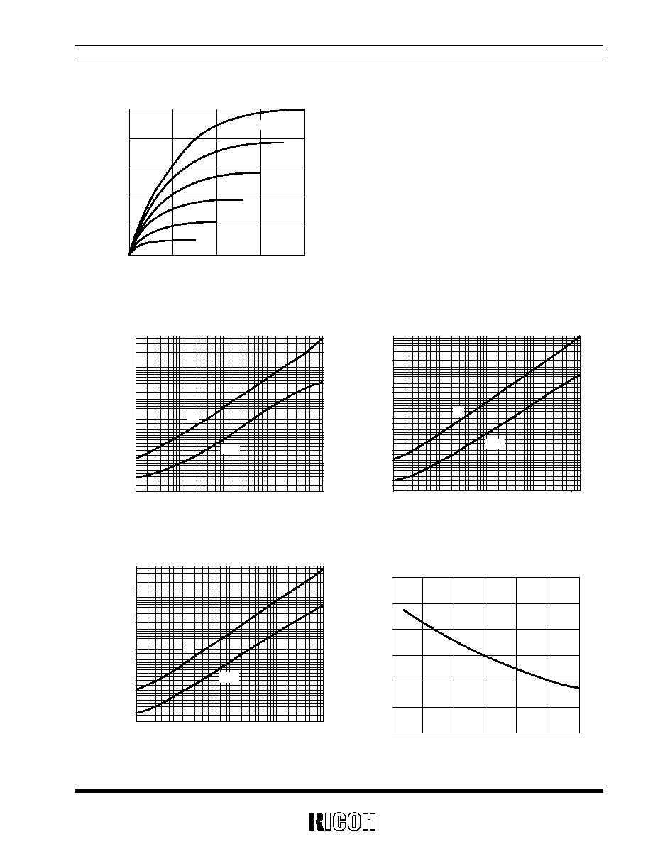
5) Nch Driver Output Current vs. Input Voltage
0
0.2
0.4
0.6
0.8
1.0
0
0.1
0.2
0.3
0.4
0.5
0.6
0.7
Output Current I
OUT
(mA)
RN5VD09x
Input Voltage V
IN
(V)
V
DS=
0.5V
Topt
=
80∞C
25∞C
≠30∞C
Output Current I
OUT
(mA)
RN5VD45x
V
DS=
0.5V
0
1
2
3
4
5
0
2
4
6
8
10
12
14
16
18
Input Voltage V
IN
(V)
Topt
=
≠
30∞C
25∞C
80∞C
Output Current I
OUT
(mA)
Input Voltage V
IN
(V)
0
0.5
1.0
1.5
2.0
2.5
3.0
0
2
4
6
8
10
12
RN5VD27x
V
DS=
0.5V
Topt
=
≠30∞C
25∞C
80∞C
6) Pch Driver Output Current vs. Input Voltage
0
2
4
6
8
10
0
0.5
1.0
1.5
2.0
2.5
3.0
3.5
4.0
Output Current I
OUT
(mA)
RN5VD09C
Input Voltage V
IN
(V)
≠0.5V
≠1.0V
≠1.5V
V
DS =
≠2.1V
0
0.5
1.0
1.5
2.0
2.5
3.0
3.5
4.0
Output Current I
OUT
(mA)
0
2
4
6
8
10
RN5VD27C
Input Voltage V
IN
(V)
V
DS =
≠2.1V
≠1.5V
≠1.0V
≠0.5V

RN5VD
21
0
2
4
6
8
10
0
0.5
1.0
1.5
2.0
2.5
3.0
3.5
4.0
Output Current I
OUT
(mA)
RN5VD45C
Input Voltage V
IN
(V)
≠0.5V
≠1.5V
V
DS =≠
2.1V
≠1.0V
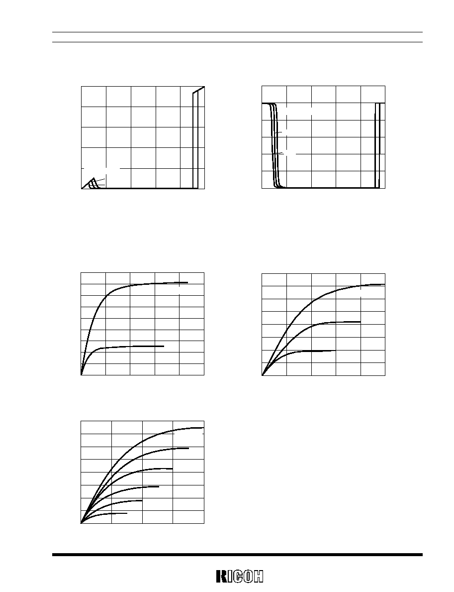
7) C
D
pin Threshold Voltage vs. Temperature
≠40
≠20
0
20
40
60
80
0.2
0.3
0.4
0.5
0.6
0.7
0.8
C
D
pin Threshold Voltage V
TCD
(V)
RN5VD09x
Temperature Topt(∞C)
V
DD=
0.99V
≠40
≠20
0
20
40
60
80
1.2
1.3
1.4
1.5
1.6
1.7
1.8
C
D
pin Threshold Voltage V
TCD
(V)
RN5VD27x
Temperature Topt(∞C)
V
DD=
2.97V
≠40
≠20
0
20
40
60
80
2.2
2.3
2.4
2.5
2.6
2.7
2.8
C
D
pin Threshold Voltage V
TCD
(V)
RN5VD45x
Temperature Topt(∞C)
V
DD=
4.95V
RN5VD
22
9) CD pin Sink Current vs. CD pin Voltage
0
0.2
0.4
0.6
0.8
1.0
0
0.02
0.04
0.06
0.08
0.10
0.12
C
D
pin Sink Current I
CD
(mA)
RN5VD09x
C
D
pin Voltage V
CD
(V)
0.7V
V
DD =
0.85V
0
0.5
1.0
1.5
2.0
2.5
0
1.5
1.0
0.5
2.0
2.5
3.0
3.5
4.0
C
D
pin Sink Current I
CD
(mA)
RN5VD27x
C
D
pin Voltage V
DS
(V)
2.0V
1.5V
V
DD =
2.5V
8) CD pin Sink Current vs. Input Voltage
0
0.2
0.4
0.6
0.8
1.0
0
0.02
0.04
0.06
0.08
0.10
0.12
0.14
0.16
0.18
C
D
pin Sink Current I
CD
(mA)
RN5VD09x
Input Voltage V
IN
(V)
25∞C
Topt
=
80∞C
≠30∞C
V
DS=
0.5V
0
1
2
3
4
5
0
1
2
3
4
5
C
D
pin Sink Current I
CD
(mA)
RN5VD45x
Input Voltage V
IN
(V)
Topt
=
≠30∞C
25∞C
80∞C
V
DS=
0.5V
0
0.5
1.0
1.5
2.0
2.5
3.0
0
0.5
1.0
1.5
2.0
2.5
3.0
C
D
pin Sink Current I
CD
(mA)
RN5VD27x
Input Voltage V
IN
(V)
Topt
= ≠
30∞C
25∞C
80∞C
V
DS=
0.5V
RN5VD
23
0
1
2
3
4
0
2
4
6
8
10
C
D
pin Sink Current I
CD
(mA)
RN5VD45x
C
D
pin Voltage V
DS
(V)
V
DD =
4.0V
3.5V
3.0V
2.5V
2.0V
1.5V
10) Output delay Time vs. External Capacitance
11) Delay Resistance vs. Temperature
0.0001
0.001
0.01
0.1
1
0.01
0.1
1
10
100
1000
Output Delay Time
t
P
(ms)
RN5VD09A
External Capacitance C
D
(µF)
t
D
t
PHL
0.0001
0.001
0.01
0.1
1
0.01
0.1
1
10
100
1000
Output Delay Time
t
P
(ms)
RN5VD27A
External Capacitance C
D
(µF)
t
D
t
PHL
0.0001
0.001
0.01
0.1
1
0.01
0.1
1
10
100
1000
Output Delay Time
t
P
(ms)
RN5VD45A
External Capacitance C
D
(µF)
t
D
t
PHL
≠40
≠20
0
20
40
60
80
0.4
0.6
0.8
1.0
1.2
1.4
1.6
Delay Resistance R
D
(M
)
RN5VDxxx
Temperature Topt(∞C)
RN5VD
24
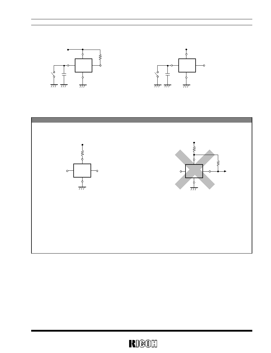
TYPICAL APPLICATIONS
∑ RN5VDxxA CPU Reset Circuit (Nch Open Drain Output)
∑ RN5VDxxC CPU Reset Circuit (CMOS Output)
∑ Memory Back-up Circuit
(1) Input Voltage to RN5VDxxA is
the same as the input voltage to CPU.
(2) Input Voltage to RN5VDxxA is
different from the input voltage to CPU.
R
V
DD
GND
OUT
C
D
C
D
RN5VDxxA
SERIES
V
DD
V
DD
CPU
RESET
GND
V
DD
V
DD1
V
DD2
GND
OUT
R
RN5VDxxA
SERIES
V
DD
CPU
RESET
GND
C
D
C
D
V
DD
V
DD
OUT
GND
RN5VDxxC
SERIES
V
DD
CPU
RESET
GND
C
D
C
D
OUT
D2
D1
A
B
G
Y1
Y2
Y3
Y4
V
CC
RAM1
GND CS
V
CC
RAM2
GND CS
V
CC
RAM3
GND CS
V
CC
RAM4
GND CS
GND
V
DD
V
DD
GND
V
CC
RN5VDxxC
SERIES
C
D
C
D
RN5VD
25
1. When RN5VDxxC (CMOS Output) is used in Fig.10,this IC may oscillate by cross conduction current at the detec-
tion when impedance is connected between Power Source V
DD
and RN5VD V
DD
Pin.When RN5VDxxA (Nch Open
Drain Output) is used in Fig.10, and R becomes excessively large, Detector Threshold may be varied because of the
voltage drop of the supply current in the IC itself.
2. The connection as shown in Fig. 11 may cause the oscillation in both RN5VDxxC (CMOS Output) and RN5VDxxA
(Nch Open Drain Output)
APPLICATION HINTS
SERIES
V
DD
V
DD
OUT
C
D
GND
RN5VD
Fig.10
SERIES
RN5VD
V
DD
V
DD
GND
OUT
R2
R1
C
D
Fig.11
∑ Manual Reset Circuit
V
DD
R
V
DD
V
DD
C
D
GND
OUT
C
D
V
DD
RN5VDxxC
SERIES
V
DD
C
D
GND
OUT
C
D
RN5VDxxA
SERIES