
PWM STEP-UP DC/DC CONVERTER
WITH VOLTAGE REGULATOR AND DETECTOR
RS5RM SERIES
APPLICATION MANUAL
NO.EA-018-0006

PWM STEP-UP DC/DC CONVERTER WITH
VOLTAGE REGULATOR AND DETECTOR
1
RS5RM SERIES
OUTLINE
The RS5RM Series are step-up DC/DC converter ICs equipped with a voltage regulator (VR) and a voltage
detector (VD) by CMOS process. Each of these step-up DC/DC converter ICs consists of a PWM DC/DC convert-
er, a linear regulator and a voltage detector. These ICs are output-voltage-fixed type regulators which function
as a linear regulator when input voltage is high, and as step-up DC/DC converter+linear regulator when input
voltage is low, by using an inductor, a diode and a capacitor as external parts for the ICs.
Since a voltage detector is built in these ICs, the potentials such as the output voltage of DC/DC converters can
be monitored.
In addition, these step-up DC/DC converter ICs are suitable for battery-powered and hand-held instruments
because internal circuits can be turned off by the chip enable function so that the standby current can be mini-
mized.
∑ Low Supply Current ..........................................TYP. 55µA (RS5RM3624A : V
IN
=3.0V,at no load)
∑ Standby Mode.....................................................Istandby=MAX. 1.0µA (RS5RM
◊◊◊◊
A)
Istandby=MAX. 10.0µA (RS5RM
◊◊◊◊
B)
∑ Low Voltage Operation Possible .......................Operating Voltage V
IN
=1.2V to 10V
∑ High Output Voltage Accuracy.........................Fixed Output Voltage Accuracy±2.5%
∑ High Voltage Detection Accuracy .....................±2.5%
∑ Output Voltage can be set at User's request (refer to Selection Guide).
∑ Voltage close to battery's voltage can be output because these ICs are of a step-up / step-down type
(Ex. a fixed voltage of 3V can be output by a 3V battery).
∑ Soft Start Function, built-in Protection Circuits for Lx Driver
∑ Phase Compensation Circuits built in
∑ Pin for External Driver is equipped, and a large current output can be obtained.
∑ Small Packages ..................................................8pin SOP
FEATURES
APPLICATIONS
∑ Power source for cameras, camcorders, and hand-held audio equipment.
∑ Power source for small OA apparatus such as note book personal computers,and word processors.
∑ Power source for hand-held communication appliances such as pagers,cordless telephones, and cellular phones.
2
RS5RM
◊◊◊◊◊
≠
◊◊
Part Number
a
b c
d
SELECTION GUIDE
In the RS5RM Series, the output voltage, the detector threshold, the version symbols, and the taping type for
the ICs can be selected at the user's request.
The selection can be made by designating the part number as shown below:
For example, the product with Output Voltage 5.0V, Detector Threshold 4.5V, Version A, and Taping Type T1,
is designated by Part Number RS5RM5045A-T1.
Code
Contens
Setting Output Voltage (V
OUT
):
a
Stepwise setting with a step of 0.1V in the range of 1.5V to 6.0V is possible.
b
Setting Detector Threshold (≠V
DET
):
Stepwise setting with a step of 0.1V in the range of 1.2V to 5.0V is possible.
Designation of Version Symbols:
c
A:
Operation of all the internal circuits is stopped by setting CE pin at V
DD
level.
B:
Operation of only Step-up DC/DC converter is stopped by setting CE pin atV
DD
level.
Designation of Taping Type:
d
Ex. 8pin SOP : T1, T2
(refer to Taping Specification)
"T2" is prescribed as a standard.
RS5RM
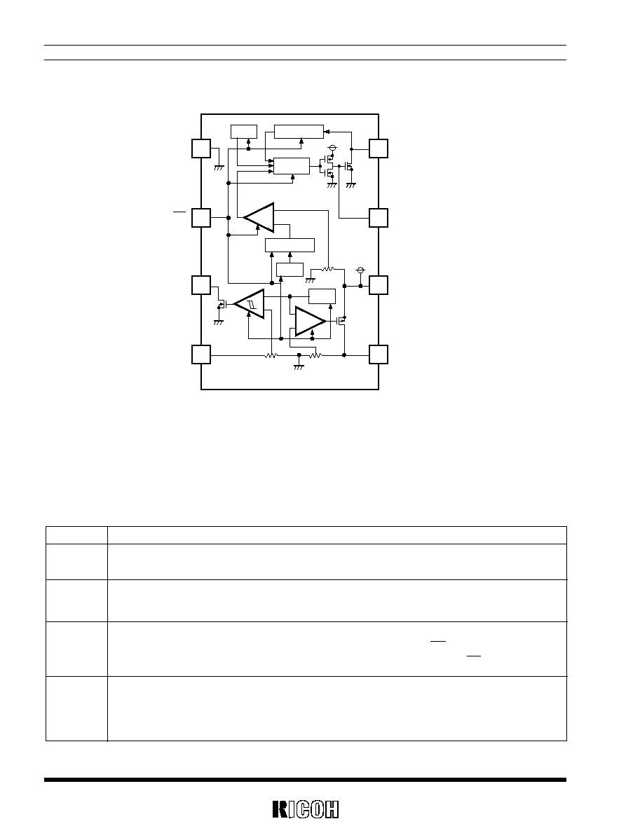
BLOCK DIAGRAM
≠
≠
≠
+
+
+
V
SS
CE
VD
OUT
VD
IN
Soft Start
Vref1
Vref2
PWM
OSC
V
LX
Limiter
1
2
3
4
5
6
7
8
L
X
EXT
V
DD
V
OUT
}
}
}

3
PIN CONFIGURATION
∑
8pin SOP
PIN DESCRIPTION
1
2
3
4
8
7
6
5
RS5RM
Pin No.
Symbol
1
V
SS
2
CE
3
VD
OUT
4
VD
IN
5
V
OUT
6
V
DD
7
EXT
8
L
X
Pin Description
Ground Pin
Chip Enable Pin
Voltage Detector Output Pin.Nch Open Drain Output
Detection Input Pin of Voltage Detector
Output Pin for Regulator
Step-up Output Pin.Power Supply Pin
External Transistor Drive Pin
External Inductor Drive Pin.
4
Topt=25∞C,Vss=0V
RS5RM
ABSOLUTE MAXIMUM RATINGS
Symbol
Item
V
DD
Supply Voltage
V
LX
L
X
Pin Voltage
V
EXT
Output Voltage
EXT Pin Voltage
V
OUT
V
OUT
Pin Voltage
VD
OUT
VD
OUT
Pin Voltage
V
CE
Input Voltage
CE Pin Voltage
VD
IN
VD
IN
Pin Voltage
A Version
B Version
I
LX
Inductor Drive Output Current
Lx Pin Current
I
EXT
EXT Pin Current
P
D
Power Dissipation
Topt
Operating Temperature Range
Tstg
Storage Temperature Range
Tsolder
Lead Temperature (Soldering)
Absolute Maximum ratings are threshold limit values that must not be exceeded even for an instant under any
conditions. Moreover, such values for any two items must not be reached simultaneously. Operation above
these absolute maximum ratings may cause degradation or permanent damage to the device. These are stress
ratings only and do not necessarily imply functional operation below these limits.
ABSOLUTE MAXIMUM RATINGS
Rating
Unit
≠ 0.3 to +12
V
Vss≠ 0.3 to +12
V
Vss ≠ 0.3 to V
DD
+0.3
V
Vss ≠0.3 to V
DD
+0.3
V
Vss≠0.3 to +12
V
Vss≠0.3 to V
DD
+0.3
V
Vss≠0.3 to V
DD
+0.3
V
Vss≠0.3 to +12
250
mA
50
mA
300
mW
≠30 to +80
∞C
≠55 to +125
∞C
260∞C, 10s

5
ELECTRICAL CHARACTERISTICS
RS5RM
∑
RS5RM3624A,B
Topt=25∞C
(Note 1) Standby current of Version A
(Note 2) Standby current of Version B
Please refer to Basic Circuit for Test Circuit.
Symbol
Item
V
IN
Operation Input Voltage
V
DD
Step-up Output Voltage
Voscst
Oscillator Start-up Voltage
Vhold
Hold-on Voltage
fosc
Oscillator Frequency
Maxdty
Oscillator Maximum Duty Cycle
V
OL
1
Lx Output Voltage
I
OH
1
Lx Leakage Current
V
LX
lim
Lx Voltage Limit
V
OH
EXT Output Pch ON Voltage
V
OL
2
EXT Output Nch ON Voltage
V
OUT
Output Voltage
V
DIF
Dropout Voltage
V
OUT
/
I
OUT
Load Regulation
≠V
DET
Detector Threshold
V
HYS
Detector Threshold Hysteresis
V
OL
3
VD
OUT
ON Voltage
I
OH
2
VD
OUT
Leakage Current
I
VDINH
VD
IN
"H" Input Current
I
VDINL
VD
IN
"L" Input Current
V
CEH
CE "H" Input Voltage
V
CEL
CE "L" Input Voltage
I
CEH
CE "H" Input Current
I
CEL
CE "L" Input Current
I
DD
Supply Current
Istandby
Standby Current
Conditions
MIN.
TYP.
MAX.
Unit
Note
No load
1.2
10
V
No load
3.99
4.1
4.21
V
No load
0.9
1.2
V
I
OUT
=1mA
0.7
V
40
50
60
kHz
65
80
90
%
I
OL
=50mA
0.5
V
0.01
10
µA
L
X
Pin On
0.9
V
I
EXT
= ≠3mA,V
DD
=4.1V
3.6
V
I
EXT
=5mA,V
DD
= 4.1V
0.5
V
I
RL
=≠5mA
3.51
3.6
3.69
V
I
RL
= ≠ 30mA
0.3
V
≠30mA
I
RL
0mA
100
mV
2.34
2.4
2.46
V
60
120
240
mV
I
OL
=5mA
0.5
V
0.01
5
µA
VD
IN
=V
DD
5
µA
VD
IN
=Vss
≠ 0.5
0.5
µA
V
DD
≠0.3
V
DD
V
0
0.2V
DD
V
CE=V
DD
≠ 0.5
0.5
µA
CE=Vss
≠ 0.5
0.5
µA
V
IN
=3V, L=100µH,
C=22µF, CE=Vss,
55
120
µA
No load
V
IN
=3V, L=100µH,
1.0
µA
Note1
C=22µF, CE=V
DD
,
No load
10.0
µA
Note2

6
RS5RM
∑
RS5RM5045A,B
Topt=25∞C
(Note 1) Standby current of Version A
(Note 2) Standby current of Version B
Please refer to Basic Circuit for Test Circuit.
Symbol
Item
V
IN
Operation Input Voltage
V
DD
Step-up Output Voltage
Voscst
Oscillator Start-up Voltage
Vhold
Hold-on Voltage
fosc
Oscillator Frequency
Maxdty
Oscillator Maximum Duty Cycle
V
OL
1
Lx Output Voltage
I
OH
1
Lx Leakage Current
V
LX
lim
Lx Voltage Limit
V
OH
EXT Output Pch ON Voltage
V
OL
2
EXT Output Nch ON Voltage
V
OUT
Output Voltage
V
DIF
Dropout Voltage
V
OUT
/
I
OUT
Load Regulation
≠V
DET
Detector Threshold
V
HYS
Detector Threshold Hysteresis
V
OL
3
VD
OUT
ON Voltage
I
OH
2
VD
OUT
Leakage Current
I
VDINH
VD
IN
"H" Input Current
I
VDINL
VD
IN
"L" Input Current
V
CEH
CE "H" Input Voltage
V
CEL
CE "L" Input Voltage
I
CEH
CE "H" Input Current
I
CEL
CE "L" Input Current
I
DD
Supply Current
Istandby
Standby Current
Conditions
MIN.
TYP.
MAX.
Unit
Note
No load
1.2
10
V
No load
5.36
5.5
5.64
V
No load
0.9
1.2
V
I
OUT
=1mA
0.7
V
40
50
60
kHz
65
80
90
%
I
OL
=50mA
0.5
V
0.01
10
µA
L
X
Pin On
0.9
V
I
EXT
=≠3mA,V
DD
=5.5V
5.0
V
I
EXT
=5mA,V
DD
=5.5V
0.5
V
I
RL
=≠5mA
4.87
5.0
5.13
V
I
RL
=≠30mA
0.3
V
≠30mA
I
RL
0mA
100
mV
4.38
4.5
4.62
V
112
225
450
mV
I
OL
=5mA
0.5
V
0.01
5
µA
VD
IN
=V
DD
5
µA
VD
IN
=Vss
≠0.5
0.5
µA
V
DD
≠0.3
V
DD
V
0
0.2V
DD
V
CE=V
DD
≠0.5
0.5
µA
CE=Vss
≠0.5
0.5
µA
V
IN
=4V, L=100µH,
C=22µF, CE=Vss,
70
150
µA
No load
V
IN
=4V, L=100µH,
1.0
µA
Note1
C=22µF, CE=V
DD
,
No load
10.0
µA
Note2

7
RS5RM
(Note) Please refer to the Application Manual for "RH5RH SERIES" for details.
OPERATION OF STEP-UP DC/DC CONVERTER
Step-up DC/DC Converter charges energy in the inductor when Lx Transistor (LxTr) is ON, and discharges the
energy with the addition of the energy from Input Power Source thereto when LxTr is OFF, so that a higher out-
put voltage than the input voltage is obtained.
The operation will be explained with reference to the following diagrams :
< Current through L >
< Basic Circuits >
i2
SD
L
X
Tr
i1
L
CL
V
IN
I
OUT
V
OUT
IL
IL min
IL max
topen
ton
toff
t
T=1/ fosc
Step.1: LxTr is turned ON and current IL (=i1 ) flows, so that energy is charged in L. At this moment, IL(=i1 ) is
increased from ILmin (=0) to reach ILmax in proportion to the on-time period (ton) of LxTr.
Step.2: When LxTr is turned OFF, Schottky diode (SD) is turned ON in order that L maintains IL at ILmax, so that
current IL (=i2) is released.
Step.3: IL (=i2) is gradually decreased, and in the case of discontinuous mode, IL reaches ILmin (=0) after a time
period of topen, so that SD is turned OFF. In the case of a continuous mode,the time period (toff) runs out
before IL reaches ILmin (=0), so that LxTr is turned ON in the next cycle, and SD is turned OFF. In this
case, ILmin does not reach zero, and IL (=i1) increases from ILmin (>0).
In the case of PWM control system, with the oscillator frequency (fosc) maintained constant, the output volt-
age is maintained constant by controlling the on-time period (ton).

8
RS5RM
≠
+
≠
+
L
X
Tr
L
X
PWM
OSC
Vref1
Vref2
Pch Tr
V
SS
100µF
100µH
V
DD
V
OUT
V
OUT
V
IN
22µF
1µF
5
1
8
6
FIG. A Diagram of RS5RM including external circuits
OPERATION
1. V
DD
Output Voltage
V
DD
output voltage is shown in Fig. B.
(1) In the case of V
IN
≠Vf
V
DD
0:
In Area B, LxTr is maintained in an OFF state, so that V
IN
≠Vf (V) is output as it is from V
DD
pin without
step-up operation.
(2) In the case of V
IN
≠Vf<V
DD
0:
In Area A, this IC functions as Step-up DC/DC converter. The step-up operation will now be explained with
reference to FIG. A. The step-up operation is an operation for regulating the V
DD
output voltage by com-
paring Vref1 and the V
DD
output voltage by error amplifier circuits and subjecting LxTr to on-time control
by PWM circuits (i.e., by controlling the step-up operation).
2. V
OUT
Output Voltage
A constant voltage is output from V
OUT
pin, with above-mentioned the V
DD
output voltage being subjected to a
step-down operation by a linear regulator. This step-down operation will now be explained with reference to FIG. A.
The step-down operation is an operation for regulating the V
DD
output voltage by Pch Tr by comparing Vref2 and
the V
DD
output voltage.
V
IN
: Input Voltage
V
DD
0
: V
DD
Set Voltage
V
OUT
0
: V
OUT
Set Voltage
Vf
: ON Voltage of Diode
Area A
V
DD
0
V
DD
Area B
V
OUT
V
DD
0+Vf
1.2V
10V
Input Voltage (V)
Output Voltage (V)
V
OUT
0
FIG. B Output Voltage vs. Input Voltage characteristic

9
RS5RM
TEST CIRCUITS
V
SS
1µF
100µF
100µH
V
OUT
V
DD
VD
IN
VD
OUT
V
IN
CE
L
X
EXT
Note1
I
IN
C
OUT
22µF
C
VDD
A
C
IN
A
V
V
Oscilloscope
V
IN
V
SS
V
OUT
V
DD
VD
IN
VD
OUT
CE
L
X
EXT
Oscilloscope
100k
Oscilloscope
V
IN
V
SS
V
OUT
V
DD
VD
IN
VD
OUT
CE
L
X
EXT
Test Circuit 1
Test Circuit 2
Test Circuit 3
100µF
100µH
V
IN
I
IN
C
IN
Digitizing Oscilloscope
Digitizing Oscilloscope
(for Trigger)
V
SS
V
OUT
V
DD
VD
IN
VD
OUT
CE
L
X
EXT
33k
A
A
+
Pulse Generator
V
SS
V
OUT
V
OUT
V
DD
VD
IN
VD
OUT
VD
IN
CE
L
X
EXT
A
OPEN
5.5V
Test Circuit 5
Test Circuit 4

10
RS5RM
1µF
100µH
V
IN
I
IN
C
IN
C
VDD
22µF
C
OUT
1µF
Digitizing Oscilloscope
V
SS
V
OUT
V
DD
VD
IN
VD
OUT
CE
L
X
EXT
100
A
A
+
+
+
Pulse Generator
Test Circuit 6
1
µ
F
C
IN
C
OUT
1
µ
F
Digitizing Oscilloscope
V
SS
V
OUT
V
DD
VD
IN
VD
OUT
CE
L
X
EXT
V
IN
Pulse
Generator
100
220
C
VDD
22
µ
F
+
100
µ
H
+
+
Test Circuit 7
I
IN
C
OUT
V
OUT
V
DD
V
SS
V
DD
V
OUT
I
OUT
I
DD
CE
EXT
V
IN
A
C
VDD
A
A
Load
NPN Tr
C
IN
Cb
Rb
D
L
RS5RM
Test Circuit 8
L
: 47µH(SUMIDA ELECTRIC CD105)
D
: Schottky Diode (HITACHI HRP22)
C
IN
: 220µF(Aluminum electrolytic Type)
Rb
: 220
Cb
: 0.01µF
C
VDD
: 220µF(Aluminum electroltic Type)
C
OUT
: 1µF(Tantalum Type)

11
RS5RM
By use of these test circuits,the typical characteristics were obtained as shown in the following pages:
Test Circuit 1: Typical Characteristics 1) 2) 3) 4) 5) 9) 10) 13) 14) 16)
(Typical Characteristics 13) and 14) were measured by replacing the capacitor shown in
Note1 with a 1µF Capacitor)
Test Circuit 2: Typical Characteristics 11) 12)
Test Circuit 3: Typical Characteristics 7) 8)
Efficiency
is shown by the following formula:
=(V
OUT
◊
I
OUT
) / (V
IN
◊
I
IN
)
Test Circuit 4: Typical Characteristics 6)
Test Circuit 5: Typical Characteristics 15)
Test Circuit 6: Typical Characteristics 17)
Test Circuit 7: Typical Characteristics 18)
Test Circuit 8: Typical Characteristics 19) 20)
In the present IC, input current at no load is defined as supply current.(CE=V
SS
).
And when CE=V
DD
, the input current (no load) is defired as standby current.

12
RS5RM
TYPICAL CHARACTERISTICS
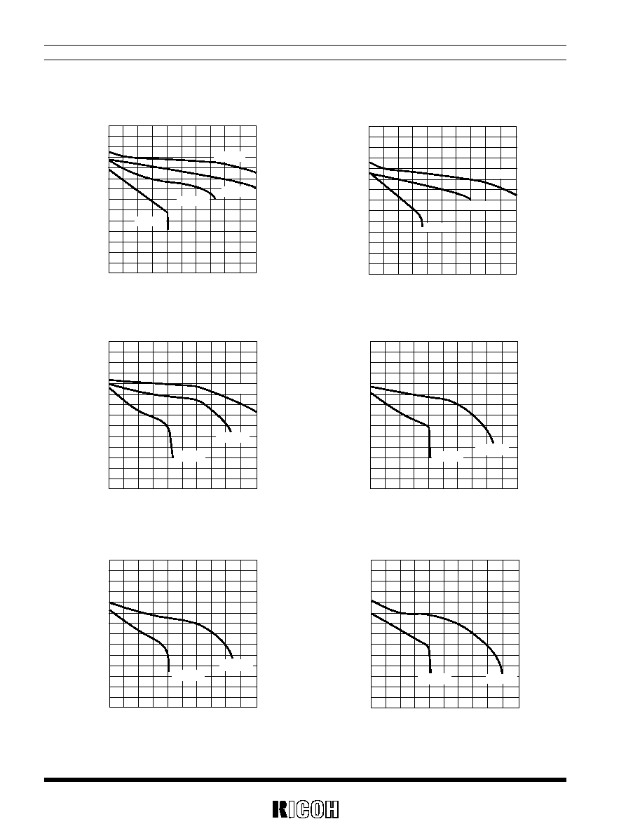
1) Output Voltage vs. Input Voltage (Topt=25∞C)
RS5RM5045A
Input Voltage V
IN
(V)
0
2
4
6
8
10
Output Voltage V
OUT
(V)
4.0
4.5
5.0
5.5
I
OUT
=10mA
I
OUT
=20mA
I
OUT
=30mA
I
OUT
=40mA
Input Voltage V
IN
(V)
0
2
4
6
8
10
Output Voltage V
OUT
(V)
3.0
3.5
4.0
4.5
I
OUT
=10mA
I
OUT
=20mA
I
OUT
=30mA
I
OUT
=40mA
RS5RM3624A
Input Voltage V
IN
(V)
0
2
4
6
8
10
Output Voltage V
OUT
(V)
2.5
3.0
3.5
4.0
I
OUT
=10mA
I
OUT
=20mA
I
OUT
=30mA
I
OUT
=40mA
RS5RM3329A
Input Voltage V
IN
(V)
0
2
4
6
8
10
Output Voltage V
OUT
(V)
2.5
3.0
3.5
4.0
I
OUT
=10mA
I
OUT
=20mA
I
OUT
=30mA
I
OUT
=40mA
RS5RM4036A
RS5RM3531A
Input Voltage V
IN
(V)
0
2
4
6
8
10
Output Voltage V
OUT
(V)
2.5
3.0
3.5
4.0
I
OUT
=10mA
I
OUT
=20mA
I
OUT
=30mA
I
OUT
=40mA
RS5RM3027A
Input Voltage V
IN
(V)
0
2
4
6
8
10
Output Voltage V
OUT
(V)
2.0
2.5
3.0
3.5
I
OUT
=10mA
I
OUT
=20mA
I
OUT
=30mA
I
OUT
=40mA

13
RS5RM
2) Output Voltage vs. Output Current (Topt=25∞C)
RS5RM5045A
Output Current I
OUT
(mA)
Output Voltage V
OUT
(V)
0
50
100
150
4.0
4.5
5.0
5.5
V
IN
=2V
V
IN
=4V
V
IN
=3V
V
IN
=5V
Output Current I
OUT
(mA)
0
50
100
150
Output Voltage V
OUT
(V)
3.0
3.5
4.0
4.5
V
IN
=2V
V
IN
=3V
V
IN
=4V
RS5RM3624A
Output Current I
OUT
(mA)
0
50
100
150
Output Voltage V
OUT
(V)
2.5
3.0
3.5
4.0
V
IN
=4V
V
IN
=3V
V
IN
=2V
RS5RM3329A
Output Current I
OUT
(mA)
0
20
40
60
80
100
Output Voltage V
OUT
(V)
2.5
3.0
3.5
4.0
V
IN
=3V
V
IN
=2V
RS5RM4036A
RS5RM3531A
Output Current I
OUT
(mA)
0
20
40
60
80
100
Output Voltage V
OUT
(V)
2.5
3.0
3.5
4.0
V
IN
=3V
V
IN
=2V
RS5RM3027A
Output Current I
OUT
(mA)
0
20
40
60
80
100
Output Voltage V
OUT
(V)
2.0
2.5
3.0
3.5
V
IN
=3V
V
IN
=2V

14
RS5RM
3) Ripple Voltage vs. Output Current (Topt=25∞C)
RS5RM5045A
Ripple Voltage Vr (mVp-p)
Output Current I
OUT
(mA)
0
10
20
30
40
50
0
5
10
15
20
25
30
35
40
45
2.0V
3.0V
4.0V
L=100µH
C
OUT
=22µF
Tantalum
V
IN
=1.2V
Output Current I
OUT
(mA)
0
10
20
30
40
50
Ripple Voltage Vr (mVp-p)
0
5
10
15
20
25
30
35
40
45
2.0V
3.0V
4.0V
L=47µH
C
OUT
=22µF
Tantalum
V
IN
=1.2V
RS5RM5045A
Output Current I
OUT
(mA)
0
10
20
30
40
50
Ripple Voltage Vr (mVp-p)
0
5
10
15
20
25
30
35
40
45
2.0V
3.0V
4.0V
L=100µH
C
OUT
=47µF
Tantalum
V
IN
=1.2V
RS5RM5045A
Output Current I
OUT
(mA)
0
10
20
30
40
50
Ripple Voltage Vr (mVp-p)
0
5
10
15
20
25
30
35
40
45
2.0V
3.0V
4.0V
L=100µH
C
OUT
=100µF
Alminum electrolytic
V
IN
=1.2V
RS5RM5045A
RS5RM5045A
Output Current I
OUT
(mA)
0
20
40
60
80
Ripple Voltage Vr (mVp-p)
0
5
10
15
20
25
30
35
40
45
2.0V
3.0V
4.0V
L=220µH
C
OUT
=22µF
Tantalum
V
IN
=1.2V

15
RS5RM
4) Efficiency vs. Input Voltage (Topt=25∞C)
RS5RM5045A
Input Voltage V
IN
(V)
Efficiency
(%)
0
2
4
6
8
10
20
40
60
80
100
I
OUT
=40mA
I
OUT
=30mA
I
OUT
=20mA
I
OUT
=10mA
Input Voltage V
IN
(V)
0
2
4
6
8
10
Efficiency
(%)
20
40
60
80
100
I
OUT
=40mA
I
OUT
=30mA
I
OUT
=20mA
I
OUT
=10mA
RS5RM3624A
Input Voltage V
IN
(V)
0
2
4
6
8
10
Efficiency
(
%)
20
40
60
80
100
I
OUT
=40mA
I
OUT
=30mA
I
OUT
=20mA
I
OUT
=10mA
RS5RM3329A
Input Voltage V
IN
(V)
Efficiency
(%)
0
2
4
6
8
10
20
40
60
80
100
I
OUT
=40mA
I
OUT
=30mA
I
OUT
=20mA
I
OUT
=10mA
RS5RM4036A
RS5RM3531A
Input Voltage V
IN
(V)
Efficiency
(%)
0
2
4
6
8
10
20
40
60
80
100
I
OUT
=40mA
I
OUT
=30mA
I
OUT
=20mA
I
OUT
=10mA
RS5RM3027A
Input Voltage V
IN
(V)
0
2
4
6
8
10
Efficiency
(%)
20
40
60
80
100
I
OUT
=40mA
I
OUT
=30mA
I
OUT
=20mA
I
OUT
=10mA
16
RS5RM
5) Efficiency vs. Output Current (Topt=25∞C)
RS5RM5045A
Efficiency
(%)
40
30
50
60
80
70
90
100
Output Current I
OUT
(mA)
0
40
60
80
20
V
IN
=5V
V
IN
=4V
V
IN
=3V
V
IN
=2V
100
V
IN
=4V
V
IN
=3V
V
IN
=2V
Efficiency
(%)
40
30
50
60
80
70
90
100
Output Current I
OUT
(mA)
0
40
60
80
20
100
RS5RM3624A
V
IN
=4V
V
IN
=3V
V
IN
=2V
Efficiency
(%)
40
30
50
60
80
70
90
100
Output Current I
OUT
(mA)
0
40
60
80
20
100
RS5RM3329A
V
IN
=3V
V
IN
=2V
Efficiency
(%)
40
30
50
60
80
70
90
100
Output Current I
OUT
(mA)
0
40
60
80
20
100
RS5RM4036A
RS5RM3531A
V
IN
=3V
V
IN
=2V
Efficiency
(%)
40
30
50
60
80
70
90
100
Output Current I
OUT
(mA)
0
40
60
80
20
100
RS5RM3027A
V
IN
=3V
V
IN
=2V
Efficiency
(%)
40
30
50
60
80
70
90
100
Output Current I
OUT
(mA)
0
40
60
80
20
100

17
RS5RM
6) Soft Start Time vs. Input Voltage (Topt=25∞C)
RS5RM5045B
C
VDD
=22µF
C
OUT
=1µF
Input Voltage V
IN
(V)
Soft Start Time Ts(ms)
0
10
20
30
40
50
60
1
2
3
4
5
6
40mA
10mA
I
OUT
=1mA
C
VDD
=22µF
C
OUT
=47µF
Soft Start Time Ts(ms)
0
10
20
30
40
50
60
Input Voltage V
IN
(V)
1
2
3
4
5
6
10mA
40mA
I
OUT
=1mA
RS5RM5045B
C
VDD
=22µF
C
OUT
=100µF
Soft Start Time Ts(ms)
0
10
20
30
40
50
60
1
2
3
4
5
6
10mA
40mA
I
OUT
=1mA
RS5RM3624A
Oscillator Maximum Duty Cycle Maxdty (%)
80
40
60
100
Temperature Topt (∞C)
≠40 ≠20
0
20
40
60
80
100
RS5RM5045B
RS5RM3624A
Oscillator Frequency F
OSC
(kHz)
10
20
80
40
60
100
Temperature Topt (∞C)
≠40 ≠20
0
20
40
60
80
100
RS5RM3624A
Output Voltage V
DD
(V)
4.1
3.7
3.9
4.3
Temperature Topt (∞C)
≠40 ≠20
0
20
40
60
80 100
7) Oscillator Frequency vs. Temperature
8) Oscillator Maximum Duty Cycle vs.Temperature
9) Output Voltage (V
DD
) vs.Temperature

18
RS5RM
10) Output Voltage vs. Temperature
RS5RM3624A
Output Voltage V
OUT
(V)
3.6
3.2
3.4
3.8
Temperature Topt (∞C)
≠40 ≠20
0
20
40
60
80
100
Detectoh Threshold V
DET
(V)
2.4
2.0
2.2
2.6
Temperature Topt (∞C)
≠40 ≠20
0
20
40
60
80
100
RS5RM3624A
0
1
2
3
4
5
VD Input Voltage VD
IN
(V)
VD Output Voltage VD
OUT
(V)
1
2
3
4
5
0
VD
IN
Pull-Up Resistor:100k
RS5RM3624
◊
Temperature Topt (∞C)
≠40 ≠20
0
20
40
60
80
100
0
1
2
3
Standby Current Istandby (µA)
B version
A version
RS5RM3624A
RS5RM
◊◊◊◊
A
Supply Current I
DD
(µA)
0
100
200
300
Input Voltage V
IN
(V)
0
2
4
6
8
10
12
5045
4036
3624
3531
3329
3027
RS5RM5045A
0.0
0.2
0.4
0.6
0.8
1.0
VD Input Current I
VDIN
(µA)
VD Input Voltage VD
IN
(V)
0
1
2
3
4
5
6
V
DD
=5.5V
13) Supply Current vs. Input Voltage
14) Standby Current vs.Temperature
15) VD Input Current vs. VD Input Voltage
11) Detector Threshold vs. Temperature
12) VD Output Voltage vs. VD Input Voltage

19
RS5RM
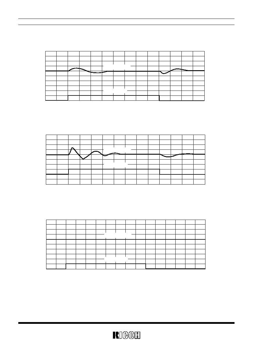
16) Start-up/Hold-on Voltage vs. Output Current
0
5
10
15
20
0
0.2
0.4
0.6
0.8
1.0
1.2
1.4
1.6
Output Current I
OUT
(mA)
Start-up/Hold-on Voltage Vstart/Vhold(V)
Vstart
Vhold
RS5RM5045A

20
RS5RM
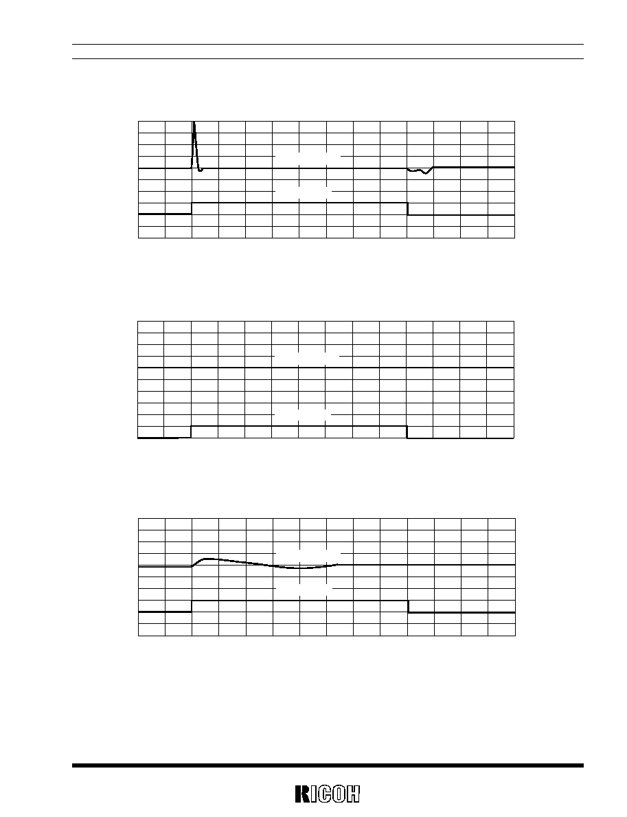
RS5RM5045A
17) Load Transient Response
≠2
0
2
4
6
8
10
12
Time t (ms)
0
1
2
3
4
5
6
Output Voltage V
OUT
(V)
0
30
60
90
120
150
180
Output Current I
OUT
(mA)
V
IN
=3.0V
C
OUT
=1µF
1mA
Output Voltage
Output Current
RS5RM5045A
≠2
0
2
4
6
8
10
12
Time t(ms)
0
1
2
3
4
5
6
Outout Voltage V
OUT
(V)
0
30
60
90
120
150
180
Output Current I
OUT
(mA)
V
IN
=5.0V
C
OUT
=1µF
Output Current
Output Voltage
1mA
RS5RM5045A
≠2
0
2
4
6
8
10
12
14
16
18
Time t (ms)
0
1
2
3
4
5
6
Output Voltage V
OUT
(V)
0
30
60
90
120
150
180
Output Current I
OUT
(mA)
V
IN
=3.0V
C
OUT
=47µF
Output Current
Output Voltage
1mA

21
RS5RM
RS5RM5045A
≠2
0
2
4
6
8
10
12
14
16
18
Time t (ms)
0
1
2
3
4
5
6
Output Voltage V
OUT
(V)
0
30
60
90
120
150
180
Output Current I
OUT
(mA)
V
IN
=5.0V
C
OUT
=47µF
Output Voltage
Output Current
1mA
RS5RM5045A
V
IN
=3.0V
C
OUT
=100µF
≠2
0
2
4
6
8
10
12
14
16
18
Time t (ms)
0
1
2
3
4
5
6
Output Voltage V
OUT
(V)
30
60
90
120
150
180
Output Current I
OUT
(mA)
Output Voltage
Output Current
1mA
RS5RM5045A
V
IN
=5.0V
C
OUT
=100µF
≠2
0
2
4
6
8
10
12
14
16
18
Time t (ms)
0
1
2
3
4
5
6
Output Voltage V
OUT
(V)
30
60
90
120
150
180
Output Current I
OUT
(mA)
Output Voltage
Output Current
1mA

22
RS5RM
RS5RM5045A
18) Line Transient Response
≠2
0
2
4
6
8
10
12
Time t (ms)
4.4
4.5
4.6
4.7
4.8
4.9
5.0
5.1
5.2
5.3
5.4
Output Voltage V
OUT
(V)
4
6
8
10
12
14
Input Voltage V
IN
(V)
I
OUT
=1mA
C
OUT
=1µF
Output Voltage
Input Voltage
RS5RM5045A
≠2
0
2
4
6
8
10
12
Time t (ms)
4.4
4.5
4.6
4.7
4.8
4.9
5.0
5.1
5.2
5.3
5.4
Output Voltage V
OUT
(V)
4
6
8
10
12
14
Input Voltage V
IN
(V)
I
OUT
=1mA
C
OUT
=1µF
Output Voltage
Input Voltage
RS5RM5045A
≠2
0
2
4
6
8
10
12
Time t (ms)
4.4
4.5
4.6
4.7
4.8
4.9
5.0
5.1
5.2
5.3
5.4
Output Voltage V
OUT
(V)
4
6
8
10
12
14
Input Voltage V
IN
(V)
I
OUT
=30mA
C
OUT
=1µF
Output Voltage
Input Voltage
23
RS5RM
RS5RM5045A
≠2
0
2
4
6
8
10
12
Time t (ms)
4.4
4.5
4.6
4.7
4.8
4.9
5.0
5.1
5.2
5.3
5.4
Output Voltage V
OUT
(V)
4
6
8
10
12
14
Input Voltage V
IN
(V)
I
OUT
=30mA
C
OUT
=1µF
Output Voltage
Input Voltage
RS5RM5045A
≠2
0
2
4
6
8
10
12
Time t (ms)
4.4
4.5
4.6
4.7
4.8
4.9
5.0
5.1
5.2
5.3
5.4
Output Voltage V
OUT
(V)
4
6
8
10
12
14
Input Voltage V
IN
(V)
I
OUT
=1mA
C
OUT
=47µF
Output Voltage
Input Voltage
RS5RM5045A
≠2
0
2
4
6
8
10
12
Time t (ms)
4.4
4.5
4.6
4.7
4.8
4.9
5.0
5.1
5.2
5.3
5.4
Output Voltage V
OUT
(V)
4
6
8
10
12
14
Input Voltage V
IN
(V)
I
OUT
=1mA
C
OUT
=47µF
Output Voltage
Input Voltage
24
RS5RM
RS5RM5045A
≠2
0
2
4
6
8
10
12
Time t (ms)
4.4
4.5
4.6
4.7
4.8
4.9
5.0
5.1
5.2
5.3
5.4
Output Voltage V
OUT
(V)
4
6
8
10
12
14
Input Voltage V
IN
(V)
I
OUT
=30mA
C
OUT
=47µF
Output Voltage
Input Voltage
RS5RM5045A
≠2
0
2
4
6
8
10
12
Time t (ms)
4.4
4.5
4.6
4.7
4.8
4.9
5.0
5.1
5.2
5.3
5.4
Output Voltage V
OUT
(V)
4
6
8
10
12
14
Input Voltage V
IN
(V)
I
OUT
=30mA
C
OUT
=47µF
Output Voltage
Input Voltage
RS5RM5045A
≠2
0
2
4
6
8
10
14
12
Time t (ms)
4.4
4.5
4.6
4.7
4.8
4.9
5.0
5.1
5.2
5.3
5.4
Output Voltage V
OUT
(V)
4
6
8
10
12
14
Input Voltage V
IN
(V)
I
OUT
=1mA
C
OUT
=100µF
Output Voltage
Input Voltage

25
RS5RM
RS5RM5045A
≠2
0
2
4
6
8
10
14
12
Time t (ms)
4.4
4.5
4.6
4.7
4.8
4.9
5.0
5.1
5.2
5.3
5.4
Output Voltage V
OUT
(V)
4
6
8
10
12
14
Input Voltage V
IN
(V)
I
OUT
=1mA
C
OUT
=100µF
Output Voltage
Input Voltage
RS5RM5045A
≠2
0
2
4
6
8
10
14
12
Time t (ms)
4.4
4.5
4.6
4.7
4.8
4.9
5.0
5.1
5.2
5.3
5.4
Output Voltage V
OUT
(V)
4
6
8
10
12
14
Input Voltage V
IN
(V)
I
OUT
=30mA
C
OUT
=100µF
Output Voltage
Input Voltage
RS5RM5045A
≠2
0
2
4
6
8
10
14
12
Time t (ms)
4.4
4.5
4.6
4.7
4.8
4.9
5.0
5.1
5.2
5.3
5.4
Output Voltage V
OUT
(V)
4
6
8
10
12
14
Input Voltage V
IN
(V)
I
OUT
=30mA
C
OUT
=100µF
Output Voltage
Input Voltage

26
RS5RM
19) Output Voltage vs. V
DD
Output Currrent
RS5RM5045A
0
100 200 300 400 500 600 700
V
DD
Output Current I
DDOUT
(mA)
4.6
4.7
4.8
4.9
5.0
5.1
5.2
5.3
5.4
5.5
5.6
Output Voltage V
OUT
/V
DD
(V)
I
OUT
=20mA
V
DD
V
OUT
2.0V
4.0V
3.0V
V
IN
=1.2V
I
OUT
=40mA
V
DD
V
OUT
2.0V
4.0V
V
IN
=1.2V
3.0V
0
100 200 300 400 500 600 700
V
DD
Output Current I
DDOUT
(mA)
4.6
4.7
4.8
4.9
5.0
5.1
5.2
5.3
5.4
5.5
5.6
Output Voltage V
OUT
/V
DD
(V)
RS5RM5045A
I
OUT
=60mA
V
DD
V
OUT
2.0V
3.0V
4.0V
V
IN
=1.2V
0
100 200 300 400 500 600 700
V
DD
Output Current I
DDOUT
(mA)
4.6
4.7
4.8
4.9
5.0
5.1
5.2
5.3
5.4
5.5
5.6
Output Voltage V
OUT
/V
DD
(V)
RS5RM5045A
I
OUT
=40mA
3.0V
4.0V
V
IN
=1.2V
0
100 200 300 400 500 600 700
V
DD
Output Current I
DDOUT
(mA)
0
10
20
30
40
50
60
70
80
90
100
Efficiency
(%)
2.0V
RS5RM5045A
RS5RM5045A
I
OUT
=20mA
2.0V
3.0V
4.0V
V
IN
=1.2V
0
100 200 300 400 500 600 700
V
DD
Output Current I
DDOUT
(mA)
0
10
20
30
40
50
60
70
80
90
100
Efficiency
(%)
RS5RM5045A
0
100 200 300 400 500 600 700
V
DD
Output Current I
DDOUT
(mA)
I
OUT
=60mA
0
10
20
30
40
50
60
70
80
90
100
Efficiency
(%)
2.0V
V
IN
=1.2V
3.0V
4.0V
20)Output Current Efficiency vs.V
DD
Output Current
=
(V
DD
◊
I
DDOUT
)+(V
OUT
◊
I
OUT
)
◊
100
V
IN
◊
I
IN
(NOTE) Efficiency
at Typical Characteristics 20) is shown by the following formula:

27
RS5RM
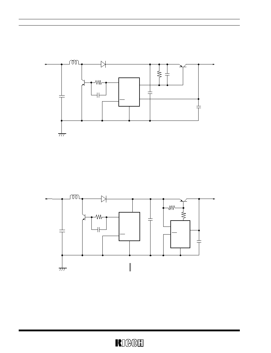
BASIC CIRCUIT
Inductor
Diode
Vss
V
OUT
+
Capacitor
EXT
V
DD
V
DD
V
IN
CE
VD
OUT
VD
IN
Lx
Examples of Parts : Inductor : RCR-664D (100µH) ; Sumida Electric Co., Ltd.
Diode
: MA721 (Schottky type) ; Matsushita Electronics Corporation
Capacitor : 22µF (Tantalum type)
28
RS5RM
TYPICAL APPLICATIONS
∑
Current Boost Circuit 1
Vss
EXT
D
RS5RM
V
DD
V
OUT
CE
V
IN
L
C
IN
NPN Tr
Rb
Cb
C
VDD
C
OUT
Rbe Cbe
PNP Tr
V
OUT
L
:47µH(SUMIDA ELECTRIC CD105)
D
:Schottky Diode (HITACHI HRP22)
C
IN
:220µF(Aluminum electrolytic Type)
Cv
DD
:100µF(Tantalum type)/
220µF(Aluminum electroltic Type)
C
OUT
:47µF(Tantalum Type)
Examples of
Components
C
D
:0.01µF
Cbe
:0.1µF(RS5RM5045
◊
,RS5RM4036
◊
,RS5RM3624
◊
)
100
P
F(RS5RM3531
◊
,RS5RM3329
◊
,RS5RM3027
◊
)
NPN Tr :2SD1628
PNP Tr :2SA1213
Rb
:220
Rbe
:12
∑
Current Boost Circuit 2 (High Efficiiency Circuit)
Vss
EXT
EXT
D
V
DD
V
DD
V
OUT
CE
CE
V
IN
L
C
IN
NPN Tr
Rb1
Cb
C
VDD
C
OUT
Rbe
PNP Tr
V
OUT
RS5RM
5 0 4 5
◊
RN5RG
50A
Rb2
GND
L
:47µH(SUMIDA ELECTRIC CD105)
D
:Schottky Diode (HITACHI HRP22)
C
IN
:220µF(Aluminum electrolytic Type)
C
VDD
:33µF(Tantalum type)/
220µF(Aluminum electroltic Type)
C
OUT
:47µF(Tantalum Type)
Examples of
Components
C
D
:0.01µF
NPN Tr :2SD1628
PNP Tr :2SA1213
Rb1
:220
Rb2
:330
Rbe
:10k
(NOTE) High efficiency current boost circuit,using RS5RM5045
◊
with
RN5RG50A(RICOH Voltage Regulator).

RS5RM
29
When using these ICs, be sure to take care of the following points:
∑
Set external components as close as possible to the IC and minimize the connection between the components
and the IC. In particular, when an external component is connected to V
OUT
Pin, make minimum connection
with the capacitor.
∑
Make sufficient grounding. A large current flows through V
SS
Pin by switching. When the impedance of the
V
SS
connection is high, the potential within the IC is varied by the switching current. This may result in
unstable operation of the IC.
∑
Use capacitor with a capacity of 10µF or more, and with good high frequency characteristics such as tantalum
capacitor. We recommend the use of a capacitor with an allowable voltage which is at least three times the
output set voltage. This is because there may be the case where a spike-shaped high voltage is generated by
the inductor when Lx transistor is turned OFF.
∑
Take the utmost care when choosing a inductor. Namely, choose such an inductor that has sufficiently small
d.c. resistance and large allowable current, and hardly reaches magnetic saturation. When the inductance
value of the inductor is small, there may be the case where I
LX
exceeds the absolute maximum ratings at the
maximum load. Use an inductor with an appropriate inductance.
∑
Use a diode of a Schottky type with high switching speed, and also take care of the rated current.
The performance of power source circuits using these ICs largely depends upon the peripheral components. Take
the utmost care in the selection of the peripheral components. In particular, design the peripheral circuits in such a
manner that the values such as voltage, current and power of each component, PCB patterns and the IC do not
exceed their respective rated values.
APPLICATION HINTS