 | –≠–ª–µ–∫—Ç—Ä–æ–Ω–Ω—ã–π –∫–æ–º–ø–æ–Ω–µ–Ω—Ç: RV5C387A | –°–∫–∞—á–∞—Ç—å:  PDF PDF  ZIP ZIP |

12345
12345
- 1 -
I
2
C-Bus Real-Time Clock ICs
with Voltage Monitoring Function
7.Jun.99
Preliminary
1. OUTLINE
The RV5C387A is a CMOS real-time clock IC connected to the CPU by two signal lines, SCL and SDA, and
configured to perform serial transmission of time and calendar data to the CPU. The periodic interrupt circuit
is configured to generate interrupt signals with six selectable interrupts ranging from 0.5 seconds to 1 month.
The 2 alarm interrupt circuits generate interrupt signals at preset times. As the oscillation circuit is driven
under constant voltage, fluctuation of the oscillator frequency due to supply voltage is small, and the time
keeping current is small (TYP. 0.35
µ
A at 3 volts). The oscillation halt sensing circuit can be used to judge
the validity of internal data in such events as power-on; The supply voltage monitoring circuit is configured to
record a drop in supply voltage below two selectable supply voltage monitoring threshold settings. The 32-
kHz clock output function (Nch open-drain output) is intended to output sub-clock pulses for the external
microcomputer. The 32-kHz clock output can be disabled by certain register settings. The oscillation
adjustment circuit is intended to adjust time counts with high precision by correcting deviations in the
oscillation frequency of the crystal oscillator. This model comes in an ultra-compact SSOP10G (Pin Pitch
0.5mm, Height1.2mm, 4.0mm
◊
2.9mm).
2. FEATURES
∑
Timekeeping supply voltage ranging from 1.45 to 5.5V
∑
Low power consumption
0.35
µ
A TYP (0.8
µ
A MAX)
at VDD=3V
∑
Only two signal lines (SCL and SDA) required for connection to the CPU.
( I
2
C-Bus Interface, 400kHz at VDD
2.5V, address7bit)
∑
Time counters (counting hours, minutes, and seconds) and calendar counters (counting years, months, days,
and weeks) (in BCD format)
∑
1900/2000 identification bit for Year 2000 compliance
∑
Interrupt circuit configured to generate interrupt signals (with interrupts ranging from 0.5 seconds to 1 month)
to the CPU and provided with an interrupt flag and an interrupt halt
∑
2 alarm interrupt circuits (Alarm_W for week, hour, and minute alarm settings and Alarm_D for hour and
minute alarm settings)
∑
32-kHz clock circuit (N-ch open-drain output)
Designed to disable 32-kHz clock output in response to a command from the host computer.
∑
Oscillation halt sensing circuit which can be used to judge the validity of internal data
∑
Supply voltage monitoring circuit with two supply voltage monitoring threshold settings
∑
Automatic identification of leap years up to the year 2099
∑
Selectable 12-hour and 24-hour mode settings
∑
Built-in oscillation stabilization capacitors (CG and CD)
∑
High precision oscillation adjustment circuit
∑
CMOS process
∑
Ultra-compact SSOP10G
*) I
2
C-Bus is a trademark of PHILIPS N.V.
Purchase of I2C-Bus components of Ricoh Company, LTD. conveys a license under the Philips I
2
C Patent
Rights to use these components in an I
2
C system, provided that the system comforms to the I
2
C standard
Specification as definded by Philips.
RV5C387A

RV5C387A PRELIMINARY
12345
- 2 -
3. PIN CONFIGURATION
SCL
SDA
/INTRA
VSS
VDD
OSCIN
/INTRB
1
2
3
4
5
6
7
9
TOP VIEW
RV5C387A (SSOP10G)
32KOUT
10
8
/INTRC
OSCOUT
4. BLOCK DIAGRAM
32kHz
OUTPUT
CONTROL
OSC
COMPARATOR_D
ALARM_D REGISTER
(MIN,HOUR)
ADDRESS
DECODER
ADDRESS
REGISTER
VOLTAGE
DETECT
DIV
TIME COUNTER
(SEC,MIN,HOUR,WEEK,DAY,MONTH,YEAR)
SHIFT REGISTER
I/O
CONTROL
32KOUT
OSCOUT
INTERRUPT CONTROL
SDA
SCL
/INTRA
DIVIDER
CORREC
-TION
VDD
VSS
COMPARATOR_W
ALARM_W REGISTER
(MIN,HOUR, WEEK)
OSCIN
OSC
DETECT
/INTRB
/INTRC
PRELIMINARY RV5C387A
12345
- 3 -
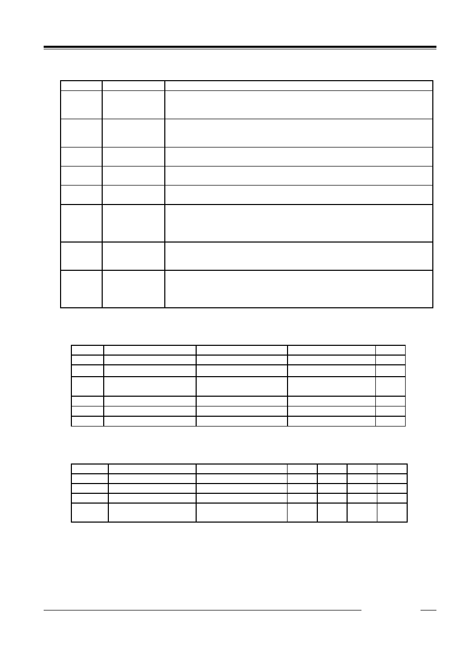
5. PIN DESCRIPTION
Symbol
Item
Description
SCL
Serial
Clock Line
The SCL pin is used to input clock pulses synchronizing the input and output
of data to and from the SDA pin. Allows a maximum input voltage of 5.5
volts regardless of supply voltage.
SDA
Serial
Data Line
The SDA pin is used to input or output data intended for writing or reading in
synchronization with the SCL pin. Up to 5.5v beyond VDD may be input.
This pin functions as an Nch open drain output.
/INTRA
Interrupt
Output A
The /INTRA pin is used to output periodic interrupt signals to the CPU.
Disabled at power-on from 0 volts. Nch. open drain output.
/INTRB
Interrupt
Output B
The /INTRB pin is used to output alarm interrupt (Alarrm_W) signals to the
CPU. Disabled at power-on from 0 volts. Nch. open drain output.
/INTRC
Interrupt
Output C
The /INTRC pin is used to output alarm interrupt (Alarm_D) signals to the
CPU. Disabled at power-on from 0 volts. Nch. open drain output.
32KOUT
32kHz Clock
Output
The 32KOUT pin is used to output 32.768-kHz clock pulses. Enabled at
power-on from 0 volts. Nch. open drain output. The RV5C387A is designed
to disable 32-kHz clock output in response to a command from the host
computer.
OSCIN
OSCOUT
Oscillation
Circuit
Input / Output
The OSCIN and OSCOUT pins are used to connect the 32.768-kHz crystal
oscillator (with all other oscillation circuit components built into the
RV5C387A).
VDD
VSS
Positive Power
Supply Input
Negative Power
Supply Input
The VDD pin is connected to the power supply.
The VSS pin is grounded.
6. ABSOLUTE MAXIMUM RATINGS
(VSS=0V)
Symbol
Item
Pin Name
Description
Unit
VDD
Supply Voltage
-0.3 to +6.5
V
VI
Input Voltage
SCL, SDA
-0.3 to +6.5
V
VO
Output Voltage
32KOUT, SDA, /INTRA,
/INTRB, /INTRC
-0.3 to +6.5
V
PD
Power Dissipation
Topt = 25
∞
C
300
mW
Topt
Operating Temperature
-40 to +85
∞
C
Tstg
Storage Temperature
-55 to +125
∞
C
7. RECOMMENDED OPERATING CONDITIONS
(VSS=0V, Topt=-40 to +85
∞
C)
Symbol
Item
Pin Name
Min,
Typ.
Max.
Unit
VDD
Supply Voltage
2.0
5.5
V
VCLK
Timekeeping Voltage
1.45
5.5
V
fXT
Oscillation Frequency
32.768
kHz
VPUP
Pull-up Voltage
SCL, SDA, /INTRA,
/INTRB, /INTRC
5.5
V
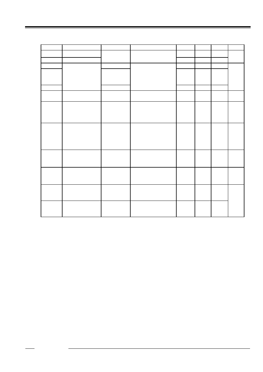
RV5C387A PRELIMINARY
12345
- 4 -
8. DC ELECTRICAL CHARACTERISTICS
(Unless otherwise specified : VSS=0V,VDD=3V,Topt=-40 to +85
∞
C)
Symbol
Item
Pin Name
Conditions
Min.
Typ.
Max.
Unit
VIH
"H" Input Voltage
0.8VDD
5.5
VIL
"L" Input Voltage
SCL,SDA
VDD=2.0 to 5.5V
-0.3
0.2VDD
V
IOL1
32KOUT
0.5
IOL2
/INTRA,
/INTRB,
/INTRC
1.0
IOL3
"L" Output
Current
SDA
VOL=0.4V
4.0
mA
IIL
Input Leakage
Current
SCL
VI=5.5V or VSS
VDD=5.5V
-1
1
µ
A
IOZ
Output Off-state
Current
SDA,
/INTRA,
/INTRB,
/INTRC
VO=5.5V or VSS
VDD=5.5V
-1
1
µ
A
IDD
Time Keeping
Current
VDD
VDD=3V,
SCL=SDA=3V,
Output = OPEN
32KOUT=OFF mode
*1)
0.35
0.8
µ
A
VDETH
Supply Voltage
Monitoring
Voltage "H"
VDD
Topt=-30 to +70
∞
C
1.90
2.10
2.30
V
VDETL
Supply Voltage
Monitoring
Voltage "L"
VDD
Topt=-30 to +70
∞
C
1.45
1.60
1.80
V
CG
Internal
Oscillation
Capacitance 1
OSCIN
12
CD
Internal
Oscillation
Capacitance 2
OSCOUT
12
pF
*1) For Standby Current for outputting 32.768kHz clock pulses from the 32KOUT pin, see, "14.7 Typical
Characteristics".
PRELIMINARY RV5C387A
12345
- 5 -
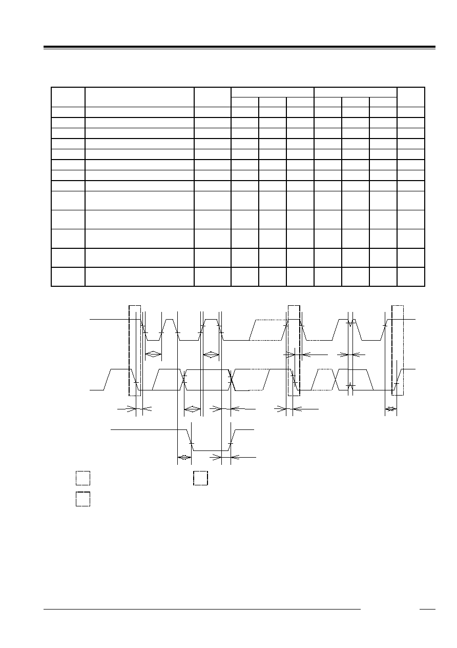
9. AC ELECTRICAL CHARACTERISTICS
Unless otherwise specified : VSS=0V,Topt=-40 to +85
∞
C
Input and Output Conditions : VIH=0.8
◊
VDD,VIL=0.2
◊
VDD,VOH=0.8
◊
VDD,VOL=0.2
◊
VDD,CL=50pF
VDD
2.0V
VDD
2.5V
Symbol
Item
Condi-
tions
Min.
Typ.
Max.
Min.
Typ.
Max.
Unit
f
SCL
SCL Clock Frequency
100
400
KHz
t
LOW
SCL Clock Low Time
4.7
1.3
µ
s
t
HIGH
SCL Clock High Time
4.0
0.6
µ
s
t
HD;STA
Start Condition Hold Time
4.0
0.6
µ
s
t
SU;STO
Stop Condition Set Up Time
4.0
0.6
µ
s
t
SU;STA
Start Condition Set Up Time
4.7
0.6
µ
s
t
SU;DAT
Data Set Up Time
250
200
ns
t
HD;DAT
Data Hold Time
0
0
ns
t
PL;DAT
SDA "L" Stable Time
After Falling of SCL
2.0
0.9
µ
s
t
PZ;DAT
SDA off Stable Time
After Falling of SCL
2.0
0.9
µ
s
t
R
Rising Time of SCL and
SDA (input)
1000
300
ns
t
F
Falling Time of SCL and
SDA (input)
300
300
ns
t
SP
Spike Width that can be
removed with Input Filter
50
50
ns
SDA(OUT)
SCL
S
Sr
P
t
PZ;DAT
t
HIGH
t
SU;DAT
t
HD;STA
t
SP
t
SU;STO
t
LOW
t
SU;STA
SDA(IN)
t
HD;STA
t
PL;DAT
Sr
P
Stop Condition
S
Start Condition
Repeated Start Condition
t
HD;DAT