 | –≠–ª–µ–∫—Ç—Ä–æ–Ω–Ω—ã–π –∫–æ–º–ø–æ–Ω–µ–Ω—Ç: BA10358 | –°–∫–∞—á–∞—Ç—å:  PDF PDF  ZIP ZIP |
1
Standard ICs
Dual ground sense operational
amplifier
BA10358 / BA10358F / BA10358FV / BA10358N
The BA10358, BA10358F, BA10358FV, and BA10358N are monolithic ICs with two independent built-in operational
amplifiers featuring high gain and frequency compensation.
These products offer a particularly wide range of operating voltages, from 3 to 32V (when using a single power
supply). Current dissipation is low and remains constant regardless of the power supply voltage. Available packages
include an 8-pin DIP (BA10358), an 8-pin SOP (BA10358F), an 8-pin SSOP-B (BA10358FV), and an 8-pin SIP
(BA10358N).
∑
Features
1) Can be driven with a single power supply.
2) Extremely low current dissipation.
3) Level is compatible with any kind of logic circuit.
4) Operating voltage range is 3 to 32V for single power
supply, ±1.5 to ±16V for dual power supply.
5) High DC voltage gain.
6) Wide frequency response.
7) Pin assignments is the same as the general-purpose
4558 model.
8) Compatible with model 358 operation amplifiers of
other manufacturers.
∑
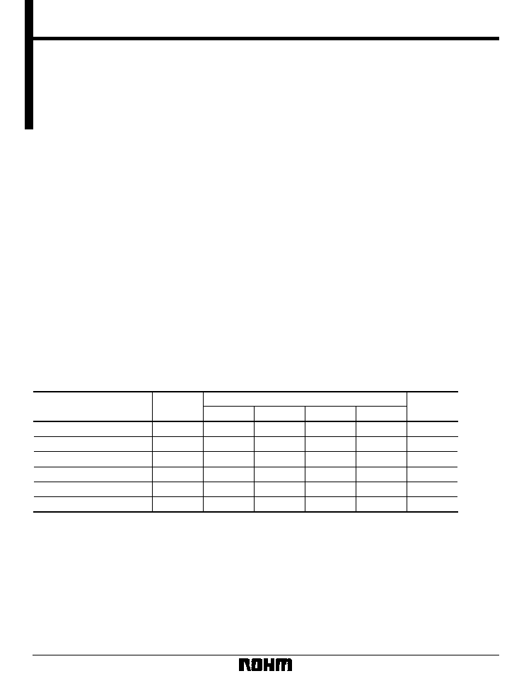
Absolute maximum ratings
Parameter
Symbol
Limits
Unit
BA10358
BA10358F
BA10358N
Power supply voltage
Power dissipation
Differential input voltage
Common-mode input voltage
Operating temperature
Storage temperature
V
CC
V
Pd
800
550
900
mW
V
ID
±
V
CC
V
V
l
≠ 0.3 ~ V
CC
≠ 40 ~ +85
≠ 55 ~ +125
V
Topr
∞
C
Tstg
∞
C
32 (
±
16)
32 (
±
16)
32 (
±
16)
32 (
±
16)
BA10358FV
350
±
V
CC
≠ 0.3 ~ V
CC
≠ 40 ~ +85
≠ 55 ~ +125
±
V
CC
≠ 0.3 ~ V
CC
≠ 40 ~ +85
≠ 55 ~ +125
±
V
CC
≠ 0.3 ~ V
CC
≠ 40 ~ +85
≠ 55 ~ +125
Refer to the Pd characteristic diagram.
The values for the BA10358F are those when it is mounted on a glass epoxy board (50mm
◊
50mm
◊
1.6mm).
The values for the BA10358FV are those when it is mounted on a glass epoxy board (70mm
◊
70mm
◊
1.6mm).
2
Standard ICs
BA10358 / BA10358F / BA10358FV / BA10358N
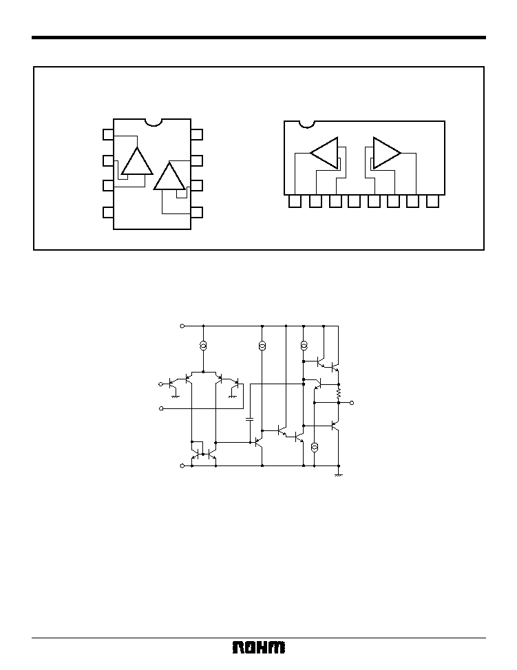
∑
Internal circuit configuration (diagram shows only one channel)
OUT
V
CC
V
EE
≠ IN
+ IN
∑
Block diagram
1ch
2ch
1
8
2
7
3
6
4
5
V
CC
OUT2
≠ 1N2
+ IN2
OUT
≠ 1N1
+ IN1
V
EE
+
≠
+
≠
1
OUT1
2
≠ IN1
3
+ IN1
4
V
EE
5
+ IN2
6
≠ IN2
7
OUT2
8
V
CC
1ch
2ch
+
≠
≠
+
BA10358 / BA10358F / BA10358FV
BA10358N

3
Standard ICs
BA10358 / BA10358F / BA10358FV / BA10358N
∑
Electrical characteristics (unless otherwise noted, Ta = 25∞C, V
CC
= +5 V)
Parameter
Symbol
Min.
Typ.
Max.
Unit
V
IO
--
2
7
mV
R
S
= 50
--
5
50
nA
--
I
B
--
45
250
nA
--
A
V
25
100
--
V
ICM
0
--
V
CC
≠ 1.5
V
--
V
O
0
--
V
CC
≠ 1.5
V
R
L
= 2k
CMRR
65
80
--
dB
--
PSRR
65
100
--
dB
R
S
= 50
I
Q
--
0.7
1.2
mA
CS
--
120
--
dB
f = 1 kHz input conversion
source
10
20
--
mA
sink
10
20
--
mA
I
IO
I
source
I
sink
Conditions
V / mV
R
L
2k
, V
CC
= 15V
R
L
=
, on All Op - Amps
V
IN
+
= 1V, V
IN
≠
= 0V, V
O
= 0V
V
IN
≠
= 1V, V
IN
+
= 0V, V
O
= V
CC
Input offset voltage
Input offset current
Input bias current
High-amplitude voltage gain
Common-mode input voltage
Output voltage
Common-mode rejection ratio
Power supply voltage rejection ratio
Quiescent current
Channel separation
Maximum
output current
∑
Electrical characteristic curves
POWER DISSIPATION: Pd (mW)
AMBIENT TEMPERATURE: Ta (
∞
C)
1200
1000
800
600
400
200
0
0
25
50
75 85 100
125
150
Fig. 1 Power dissipation vs. ambient
temperature
BA10358N
BA10358
BA10358F
BA10358FV
SUPPLY CURRENT: I
Q
(mA)
POWER SUPPLY VOLTAGE: V
+
(V)
3
2
1
0
10
20
30
40
V
CC
A
I
Q
≠
+
Fig. 2 Quiescent current vs. power
supply voltage
OPEN LOOP VOLTAGE GAIN: Av (dB)
FREQUENCY: f (Hz)
140
120
20
100
80
60
40
0
10
100
1k
1
10k
100k
1M 10M
10M
V
0
2
V
CC
V
IN
0.1
µ
Fig. 3 Open loop voltage gain vs.
frequency
+
≠
MAXIMUM OUTPUT VOLTAGE: V
OM
(V)
FREQUENCY: f (Hz)
20
15
10
0
100
1k
10k
100k
1M
100k
Vo
V
IN
2k
≠
+
1k 15V
7V
Fig. 4 Maximum output voltage
vs.frequency
INPUT BIAS CURRENT: I
R
(nA)
AMBIENT TEMPERATURE: Ta (
∞
C)
0
≠ 20
0
20
40
60
80
20
40
60
80
100
Fig. 5 Input bias current vs. ambient
temperature
INPUT BIAS CURRENT: I
a
(nA)
POWER SUPPLY VOLTAGE: V
+
(V)
0
0
10
20
30
40
25
50
75
100
Fig. 6 Input bias current vs. power
supply voltage

4
Standard ICs
BA10358 / BA10358F / BA10358FV / BA10358N
∑
Operation notes
(1) Handling unused circuits
If there are any circuits which are not being used,
we recommend making connections as shown in
Figure 10, with the non-inverted input pin
connected to the potential within the in-phase
input voltage range (V
ICM
).
OUTPUT VOLTAGE
REFERENCED TO V
+
:
V (V)
OUTPUT SOURCE CURRENT (mA)
4
5
3
2
1
0
0.001
0.01
0.1
1.0
10
100
Fig. 7 Voltage difference during power
supply output vs. output source
current
OUTPUT VOLTAGE: V
O
(V)
OUTPUT SINK CURRENT: I
O
(mA)
0.01
0.1
1.0
10
0.001
0.01
0.1
1.0
10
100
1000
Fig. 8 Output voltage vs. output sink
current
R
L
2k
V
CC
= 15V
4
3
2
1
0
0
0
20
40
60
80
1
2
3
TIME (
µ
s)
INPUT VOLTAGE OUTPUT VOLTAGE
V
IN
(V) V
OUT
(V)
Fig. 9 Output response characteristics
V
CC
V
EE
+
≠
Fig. 10 Handling unused circuits
To potential in
V
ICM
5
Standard ICs
BA10358 / BA10358F / BA10358FV / BA10358N
∑
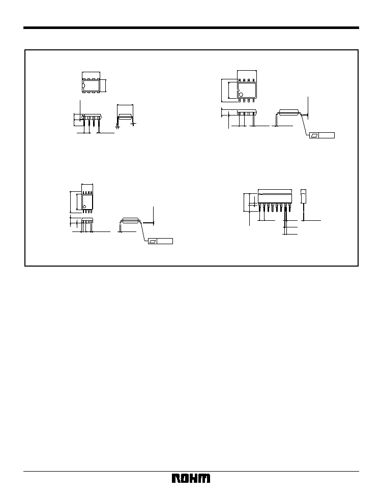
External dimensions (Units: mm)
BA10358
BA10358F
DIP8
SOP8
SIP8
SSOP-B8
BA10358N
BA10358FV
0.5
±
0.1
3.2
±
0.2
3.4
±
0.3
8
5
1
4
9.3
±
0.3
6.5
±
0.3
0.3
±
0.1
0.51Min.
2.54
0
∞
~ 15
∞
7.62
0.4
±
0.1
1.27
0.15
0.3Min.
0.15
±
0.1
0.11
6.2
±
0.3
4.4
±
0.2
5.0
±
0.2
8
5
4
1
1.5
±
0.1
0.1
0.22
±
0.1
0.65
0.3Min.
5
4
8
1
6.4
±
0.3
4.4
±
0.2
3.0
±
0.2
1.15
±
0.1
0.15
±
0.1
0.1
(0.52)
10.5
±
0.5
1
8
2.54
3.5
±
0.5
1.3
0.8
0.6
0.3
±
0.1
2.8
±
0.2
19.3
±
0.2
1.2
5.8
±
0.2