 | –≠–ª–µ–∫—Ç—Ä–æ–Ω–Ω—ã–π –∫–æ–º–ø–æ–Ω–µ–Ω—Ç: BA15218F | –°–∫–∞—á–∞—Ç—å:  PDF PDF  ZIP ZIP |

1
Standaed ICs
Dual high slew rate, low noise
operational amplifier
BA15218 / BA15218F / BA15218N
The BA15218, BA15218F, and BA15218N are monolithic ICs with two built-in low-noise, low-distortion operational
amplifiers featuring internal phase compensation.
Either a dual or single power supply can be driven, and these products can be driven by a digital system 5V single
power supply.
The following packages are available: 8-pin DIP (BA15218), 8-pin SOP (BA15218F), and 8-pin SIP (BA15218N).
1) Low-voltage operation and single power supply drive
enabled.
(Single power supply: 4 to 32V, dual power supply:
±3 to ±16V)
2) Low noise level. (Vn = 1.0
µ
V
rms
typ. : RIAA)
3) High slew rate. (SR = 3V /
µ
s, GBW = 10MHz typ.)
4) Low offset voltage. (V
IO
= 0.5mV typ.)
5) High gain and low distortion. (G
VO
= 110dB, THD =
0.0015%)
6) Pin connections are the same as with standard dual
operational amplifiers, and outstanding characteris-
tics make these products compatible with the 4558
and 4560 models.
∑
Block diagram
≠
+
+
≠
1
2
3
4
8
7
6
5
OUT1
≠ IN1
+ IN1
V
EE
V
CC
OUT2
≠ IN2
+ IN2
1ch
2ch
≠
+
≠
+
1
OUT1
2
≠ IN1
3
+ IN1
4
V
EE
5
+ IN2
6
≠ IN2
7
OUT2
8
V
CC
2ch
1ch
BA15218 / BA15218F
BA15218N
∑
Features
2
Standaed ICs
BA15218 / BA15218F / BA15218N
∑
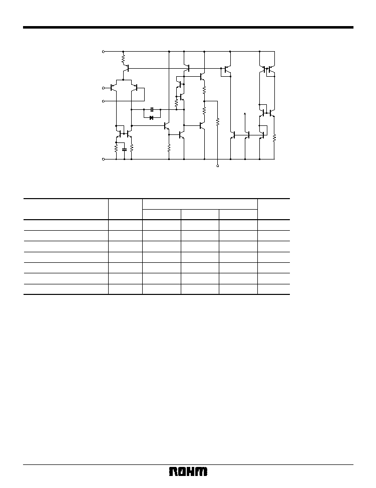
Internal circuit configuration
V
CC
V
EE
Q
3
R
2
R
3
R
4
Q
4
D
1
C
2
Q
6
Q
7
Q
10
Q
9
C
1
R
1
Q
5
Q
8
Q
11
Q
13
R
6
R
7
Q
12
Q
1
≠ IN
+ IN
Q
2
R
5
Q
14
Q
15
Q
16
OTHER
CH
Q
17
R
8
Q
19
Q
18
R
9
OUT
∑
Absolute maximum ratings (Ta = 25∞C)
Parameter
Symbol
Limits
Unit
BA15218
BA15218F
BA15218N
Power supply voltage
Power dissipation
Differential input voltage
Common-mode input voltage
Operating temperature
Storage temperature
V
CC
±
18
±
18
±
18
V
800
550
900
mW
V
ID
±
V
CC
V
V
I
≠ V
CC
~ V
CC
V
Load current
I
OMAX
±
50
±
50
±
50
mA
Topr
≠ 40
~ + 85
≠ 40
~ + 85
≠ 40
~ + 85
∞
C
Tstg
≠ 55
~ + 125
≠ 55
~ + 125
≠ 55
~ + 125
∞
C
Pd
±
V
CC
≠ V
CC
~ V
CC
±
V
CC
≠ V
CC
~ V
CC
Refer to Pd characteristics diagram.
The values for the BA15218F are those when it is mounted on a glass epoxy board (50mm
◊
50mm
◊
1.6mm).
3
Standaed ICs
BA15218 / BA15218F / BA15218N
∑
Electrical characteristics (unless otherwise noted, Ta = 25∞C, V
CC
= +15V, V
EE
= -15V)
Parameter
Symbol
Min.
Typ.
Max.
Unit
Conditions
Input offset voltage
Input offset current
Input bias current
High-amplitude voltage gain
Common-mode input voltage
Maximum output voltage
Maximum output voltage
Common-mode rejection ratio
Power supply voltage rejection ratio
Quiescent current
Slew rate
Channel separation
Voltage gain band width
Input conversion noise voltage
V
IO
--
0.5
5
mV
R
S
10k
I
IO
--
5
200
nA
--
I
B
--
50
500
nA
--
A
V
86
110
--
dB
V
ICM
±
12
±
14
--
V
--
V
OH
±
12
±
14
--
V
R
L
10k
V
OL
±
10
±
13
--
V
R
L
2k
CMRR
70
90
--
dB
R
S
10k
PSRR
76
90
--
dB
R
S
10k
I
Q
--
5
8
mA
S.R.
--
3
--
CS
--
120
--
dB
f = 1kHz input conversion
GBW
--
10
--
MHz
f = 10kHz
V
n
--
1.0
--
µ
V
rms
V /
µ
s
R
L
2k
, V
O
=
±
10V
V
IN
= 0V, R
L
=
A
V
= 1, R
L
= 2k
RIAA, R
S
= 1k
, 10Hz ~ 30kHz
∑
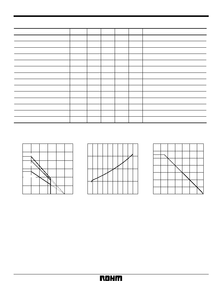
Electrical characteristic curves
POWER DISSIPATION: Pd (mW)
AMBIENT TEMPERATURE: Ta (
∞
C)
1200
1000
800
600
400
200
0
0
25
50
75
100
125
150
BA15218F
BA15218
BA15218N
Fig.1 Power dissipation vs. ambient
temperature
85
QUIESCENT CURRENT: I
Q
(mA)
POWER SUPPLY VOLTAGE: V
±
(V)
6
8
4
2
0
0
±
10
±
20
Fig.2 Quiescent current vs. power
supply voltage
OPEN LOOP VOLTAGE GAIN: A
v
(dB)
FREQUENCY: f (Hz)
140
20
40
60
80
100
120
0
1
10
100
1k
10k
100k
1M
10M
Fig.3 Open loop voltage gain vs.
frequency
4
Standaed ICs
BA15218 / BA15218F / BA15218N
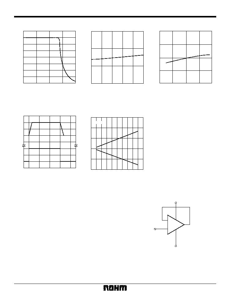
MAXIMUM OUTPUT VOLTAGE: V
OM
(V)
FREQUENCY: f (Hz)
32
4
8
12
16
20
24
28
0
100
1k
10k
100k
1M
Fig.4 Maximum output voltage vs.
frequency
INPUT BIAS CURRENT: I
B
(nA)
AMBIENT TEMPERATURE: Ta (
∞
C)
20
40
60
80
≠ 20
0
20
40
60
80
Fig.5 Input bias current vs.
ambient temperature
INPUT BIAS CURRENT: I
B
(nA)
POWER SUPPLY VOLTAGE: V
+
(V)
10
100
75
50
25
20
30
0
40
Fig.6 Input bias current vs.
power supply voltage
INPUT VOLTAGE OUTPUT VOLTAGE
V
IN
(V) V
OUT
(V)
TIME (
µ
s)
0
≠ 5
5
≠ 5
5
0
20
30
40
10
0
Fig.7 Output response characteristics
MAXIMUM OUTPUT VOLTAGE: V
OM
(V)
POWER SUPPLY VOLTAGE: V
±
(V)
30
≠ 20
≠ 10
0
10
20
0
±
10
±
20
R
L
= 2k
Fig.8 Maximum output voltage vs.
power supply voltage
∑
Operation notes
(1) Unused circuit connections
If there are any circuits which are not being used, we
recommend making connections as shown in Figure 9,
with the non-inverted input pin connected to the poten-
tial within the in-phase input voltage range (V
ICM
).
V
CC
V
EE
+
≠
To potential
in V
ICM
Fig.9 Unused circuit connections
5
Standaed ICs
BA15218 / BA15218F / BA15218N
∑
External dimensions (Units: mm)
DIP8
SOP8
SIP8
BA15218
BA15218F
BA15218N
0.5
±
0.1
3.2
±
0.2
3
.4
±
0.3
8
5
1
4
9.3
±
0.3
6.5
±
0.3
0.3
±
0.1
0.51Min.
2.54
0
∞
~15
∞
7.62
0.4
±
0.1
1.27
0.15
0.3Min.
0.15
±
0.1
0.11
6.2
±
0.3
4.4
±
0.2
5.0
±
0.2
8
5
4
1
1.5
±
0.1
10.5
±
0.5
1
8
2.54
3.5
±
0.5
1.3
0.8
0.6
0.3
±
0.1
2.8
±
0.2
19.3
±
0.2
1.2
5.8
±
0.2