1
Standard ICs
Dual high slew rate operational
amplifier
BA4510F / BA4510FV
The BA4510F and BA4510FV are monolithic ICs that contain two operational amplifiers with high slew rate, featuring
phase compensation. These ICs can be driven with a low-voltage power supply, requiring a power supply range of
± 1 to ± 3.5V for a dual power supply and 2 to 7V for a single power supply. In addition, an unbuffered type is used
which enables ample output even in low voltage ranges, enabling swing at up to nearly the power supply voltage.
∑
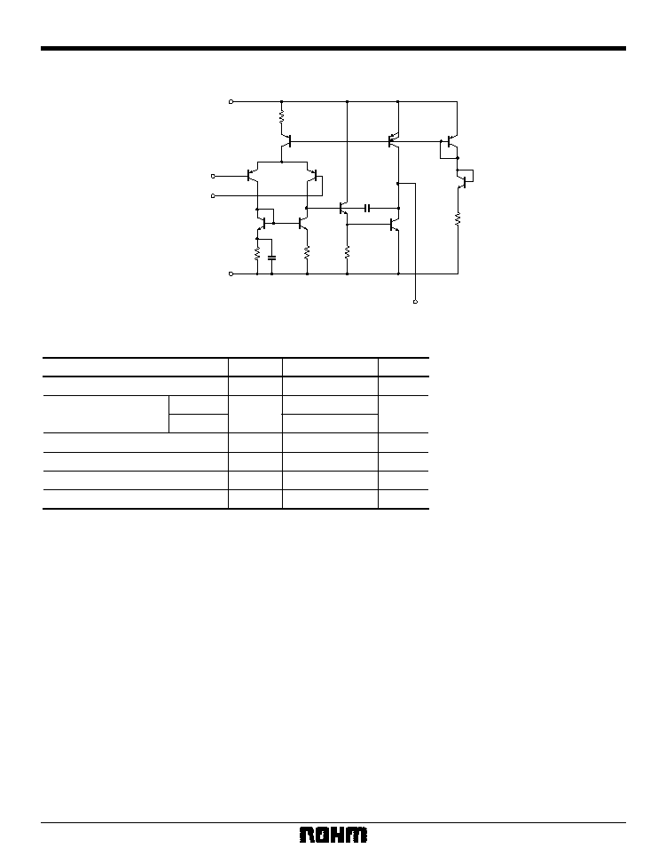
Block diagram
+
+
1
2
3
4
8
7
6
5
OUT1
≠ IN1
+ IN1
V
EE
V
CC
OUT2
≠ IN2
+ IN2
1ch
2ch
≠
≠
∑
Features
1) Low-voltage operation.
2) High slew rate.
3) Wide dynamic output range.
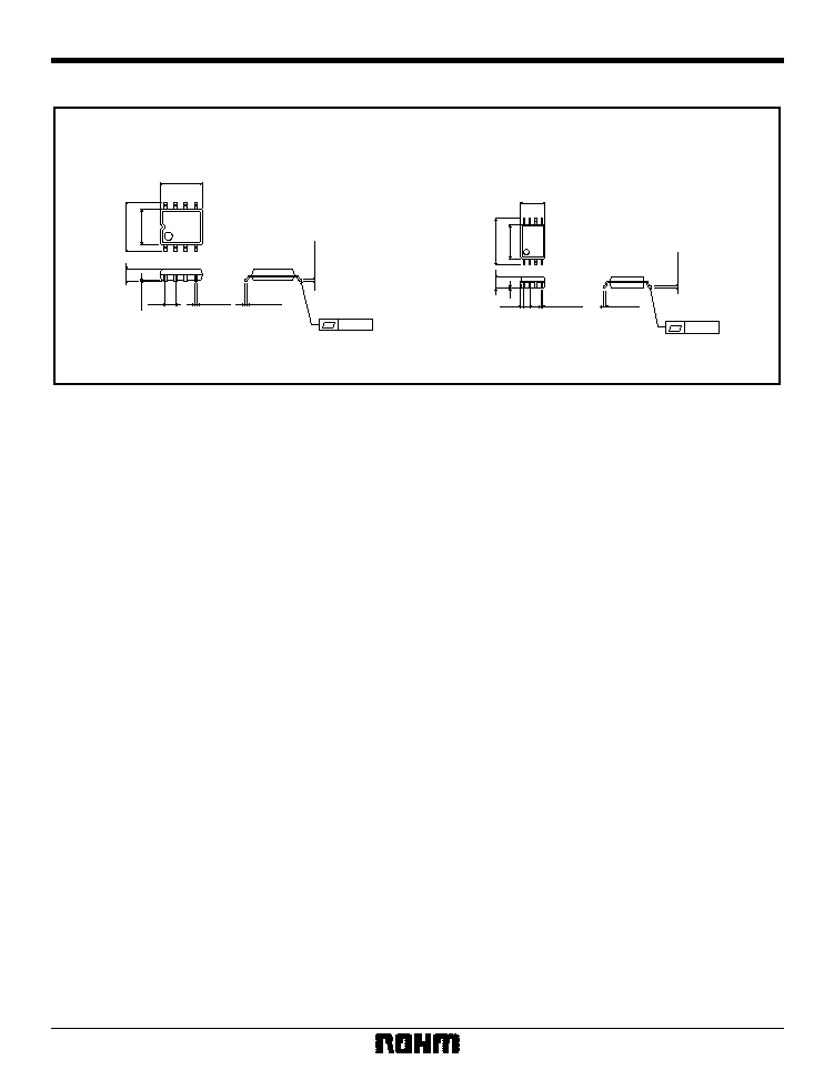
4) Compact 8-pin SSOP-B package. (BA4510FV)
2
Standard ICs
BA4510F / BA4510FV
∑
Internal circuit configuration
V
CC
V
EE
R
2
R
3
A
R
1
Q
7
Q
1
≠ IN
+ IN
Q
2
OUT
R
4
X
3
X
2
Q
8
R
5
Q
9
∑
Absolute maximum ratings (Ta = 25∞C)
Parameter
Symbol
Limits
Unit
Power supply voltage
V
CC
±
5
V
Power dissipation
BA4510F
BA4510FV
550
1
(SOP)
350
2
(SSOP)
mW
Differential input voltage
V
ID
±
V
CC
V
Common-mode input voltage
V
I
0 ~ V
CC
V
Operating temperature
Topr
∞
C
Storage temperature
Tstg
∞
C
Pd
≠ 20 ~ + 75
≠ 40 ~ + 125
1 If used at temperatures higher than 25
∞
C, reduce power by 5.5mW for each 1
∞
C above Ta = 25
∞
C.
This value is the value measured when mounted on a glass epoxy board (50mm
◊
50mm
◊
1.6mm).
2 If used at temperatures higher than 25
∞
C, reduce power by 3.5mW for each 1
∞
C above Ta = 25
∞
C.
This value is the value measured when mounted on a glass epoxy board (70mm
◊
70mm
◊
1.6mm).
The value is 300mW when the IC is used alone.
3
Standard ICs
BA4510F / BA4510FV
∑
Electrical characteristics (unless otherwise noted, Ta = 25∞C, V
CC
= ±2.5V)
Parameter
Symbol
Min.
Typ.
Max.
Unit
Input offset voltage
V
IO
--
1
6
mV
R
S
= 50
Input offset current
I
IO
--
2
200
nA
Input bias current
I
B
--
80
500
nA
High-amplitude voltage gain
A
V
60
90
--
dB
Common-mode input voltage
V
ICM
≠ 1.3
--
V
Common-mode rejection ratio
CMRR
60
80
--
dB
Power supply voltage rejection ratio
PSRR
60
80
--
dB
R
S
= 50
Quiescent current
I
Q
2.5
5.0
7.5
mA
Output voltage
High
V
OH
2.0
2.4
--
V
R
L
= 2k
Low
V
OL
--
≠ 2.4
≠ 2.0
V
R
L
= 2k
Slew rate
S.R.
5
V /
µ
s
--
1.5
--
Conditions
R
L
2k
, V
CC
= 15V
R
L
=
ALL AMPS
1
1 Because the first stage is configured with a PNP transistor, input bias current is from the IC.
∑
Electrical characteristic curve
POWER DISSIPATION: Pd (mW)
AMBIENT TEMPERATURE: Ta (
∞
C)
1200
1000
800
600
400
200
0
0
25
50
75
100
125
150
BA4510F
BA4510FV
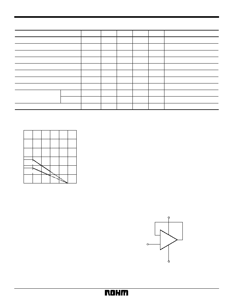
Fig. 1 Power dissipation vs. ambient
temperature
∑
Operation notes
(1) Unused circuit connections
If there are any circuits which are not being used, we
recommend making connections as shown in Figure 2,
with the non-inverted input pin connected to the poten-
tial within the in-phase input voltage range (V
ICM
).
(2) If used with a voltage follower, be careful of oscilla-
tion which may cause problems with the in-line input
voltage range or the capacitance load.
(3) If using at power supply voltage + 5.0 or higher, be
sure the gain is reduced sufficiently to prevent oscilla-
tion.
V
CC
V
EE
To potential
in V
ICM
+
≠
Fig. 2 Unused circuit connections