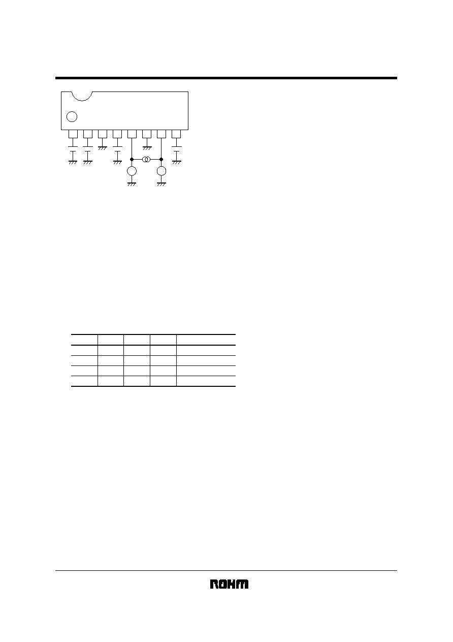
BA6283N / BA6955N
Motor driver ICs
Reversible motor driver
BA6283N / BA6955N
The BA6283N and BA6955N are reversible-motor drivers with a maximum output current of 1.0A. Two logic inputs allow
four output modes: forward, reverse, stop (standby), and brake.
The built-in power save circuit suppresses current consumption in the motor stop mode.
!
!
!
!
Applications
VCRs, audio devices
!
!
!
!
Features
1) Logic and driver sections have separate ground pins; this allows the IC to drive speed-variable, reversible motors by
connecting an electronic governor circuit.
2) Built-in power saving circuit suppresses current consumption in stop (standby) mode.
3) Interfaces with TTL devices.
4) Built-in thermal shutdown circuit.
!
!
!
!
Absolute maximum ratings (Ta = 25
°C)
Parameter
Symbol
Limits
Unit
Applied voltage
V
CC
18
V
Power dissipation
Pd
BA6283N
BA6955N
1150
1
1080
2
mW
Operating temperature
Topr
-
20~
+
75
°
C
Output current
I
OUT
1000
3
mA
Storage temperature
Tstg
-
55~
+
150
°
C
1 Reduced by 9.2mW for each increase in Ta of 1
°
C over 25
°
C.
2 Reduced by 8.64mW for each increase in Ta of 1
°
C over 25
°
C.
3 Should not exceed Pd or ASO values.
!
!
!
!
Recommended operating conditions (Ta = 25
°C)
Parameter
Operating power supply voltage
V
CC
5.5
15
V
-
V
M
5.5
15
V
-
Symbol
Min.
Typ.
Max.
Unit
BA6283N / BA6955N
Motor driver ICs
!
!
!
!
Pin descriptions
BA6283N
Pin No.
Functions
Power supply
Pin name
V
CC
1
2
3
4
5
6
7
9
8
Logic input
F
IN
GND
GND
GND
GND
Motor output
OUT2
Logic input
Motor output
Motor power supply
Output GND, for connecting resistor for output current detection
R
IN
R
NF
V
M
OUT1
BA6955N
Pin No.
Functions
Power supply
Pin name
V
CC
1
2
3
4
5
6
7
8
Logic input
F
IN
GND
GND
Motor output
OUT2
Logic input
Motor output
Motor power supply
Output GND, for connecting resistor for output current detection
R
IN
R
NF
V
M
OUT1
!
!
!
!
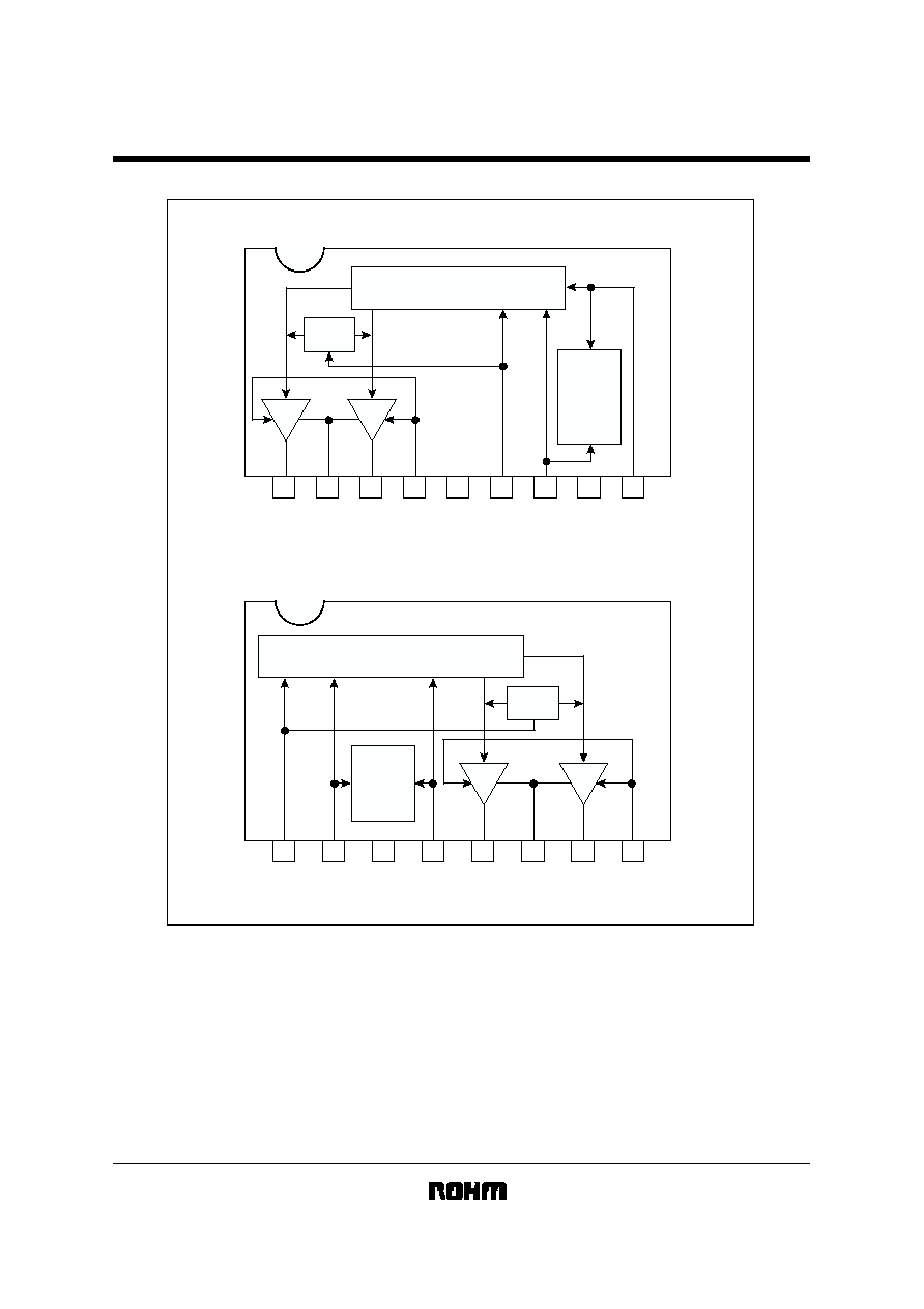
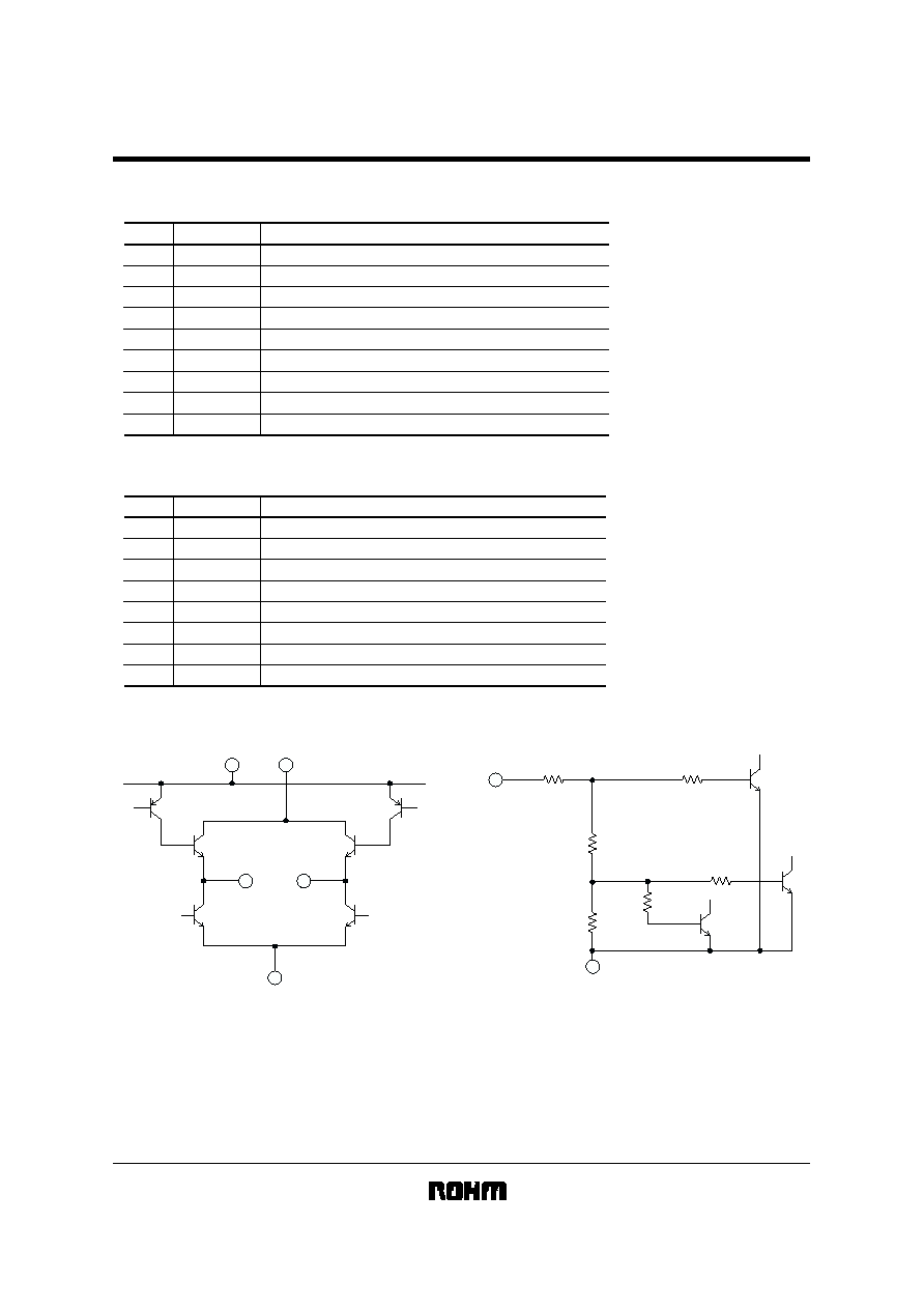
Input / Output circuit
Fig.1
V
CC
V
M
OUT1
R
NF
OUT2
Fig.2
GND
F
IN
R
IN
12k
11k
11k
10k
20k
4.7k
Resistances are typical values
BA6283N / BA6955N
Motor driver ICs
!
!
!
!
Electrical characteristics (unless otherwise noted, Ta=25
°C, V
CC
=9V, and V
M
=9V)
Parameter
Symbol
Min.
I
CC
1
I
CC
2
I
CC
3
V
IH
V
IL
I
IH
V
CE
-
-
-
2.0
-
-
50
Typ.
-
-
-
30
40
90
1.0
Max.
Unit
15
43.5
58
µ
A
-
0.8
V
V
V
mA
mA
130
1.5
µ
A
Conditions
Circuit current1
Circuit current2
Circuit current3
Input high level voltage
Input low level voltage
Input high level current
Output saturation voltage
Not designed for radiation resistance.
Standby mode
-
-
Forward or reverse mode
Brake mode
V
IN
=2.0V
I
O
=200mA
Sum of the high and low side output
transistor voltages
!
!
!
!
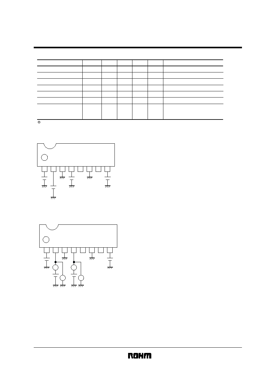
Measuring circuits
V
CC
I
CC
V
IR
V
IF
V
M
Fig.3
Refer to the Input/Output truth table about the output mode.
Circuit current : I
CC
A
V
A
V
V
CC
I
IH
I
IH
V
IR
V
IF
V
M
Fig.4
Input high level voltage, Input low level voltage
Refer to the Input/Output truth table about the output mode.
: V
IF
, V
IR
Input high level current
: I
IH
at V
IF
=2V, I
IH
at V
IR
=2V
BA6283N / BA6955N
Motor driver ICs
V
V
V
CC
V
IR
V
OF
V
OR
V
IF
V
M
Fig.5
V
CE
: Sum of the high and low side output transistor voltage.
I
O
flows from High to Low Level output pins.
!
!
!
!
Circuit operations
(1) Input section (F
IN
, R
IN
)
Control signals are input from these pins. Input circuit can be controlled with TTL or over voltage input.
Operation in each mode is show below.
Output current flows from OUT1 to OUT2 (forward mode) when F
IN
is High and R
IN
is Low, and from OUT2 to OUT1
(reverse mode) when R
IN
is Low and R
IN
is High. Putting F
IN
and R
IN
both High result in the brake mode. In this mode,
the high-side output transistor is turned off to shut down the motor driving current and the low-side output transistor is
turned on to absorb the counter-electromotive force of the motor. When F
IN
and R
IN
are both Low, both OUT1 and
OUT2 are left open and the motor stops. In this mode the power save circuit turn to active, and whole the IC circuit off
cause the circuit current to minimize.
Input / output truth table
F
IN
H
L
H
L
R
IN
L
H
H
L
OUT1
H
L
L
OPEN
OUT2
L
H
L
OPEN
Mode
Forward
Reverse
Brake
Standby
(2) Output section (OUT1, OUT2)
Two logic inputs control the motor by changing the status of the bridge-configured transistors.
(3) Power supply section (V
CC
, V
M
)
V
CC
is a logic Power supply terminal, and V
M
is a Motor Power supply terminal.
(4) Thermal shut down (TSD)
When the IC internal temperature rises by the accident motor locked, the thermal shut down circuit is activated and all
the outputs turn off with regardless of input mode. Then, the temperature fulls and the thermal shut down circuit is
disactirated, the output returns with regard of the input mode.
This circuit is activated when the IC junction temperature rises above 175
°C (Typ.) and disabled when it is 150°C
(Typ.).
(5) Power save circuit
When F
IN
and R
IN
are both Low, all the IC circuit turns off and it decrease the IC consumption current.