700
Motor driver ICs
2-phase half-wave motor driver
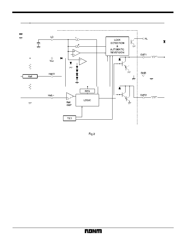
BA6407AF
The BA6407AF is a motor driver dedicated to 12V fan motors. Built-in output transistors reduce the number of external
components required. The IC has a lock signal output pin.
F
Applications
Fan motors
F
Features
1) Lock detection and rotational speed sensing mecha-
nisms are built in.
2) Compact SOP 8-pin package reduces the number of
external components required.
3) Automatic restart when the motor lock is undone.
F
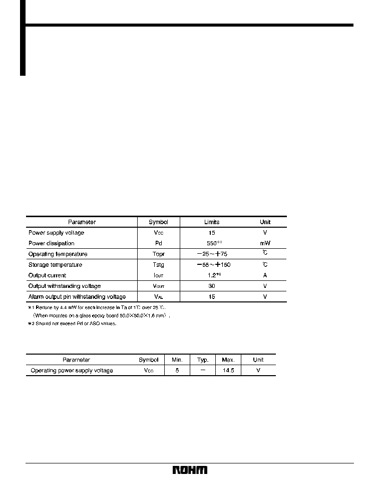
Absolute maximum ratings (Ta = 25
_
C)
F
Recommended operating conditions (Ta = 25
_
C)
702
Motor driver ICs
BA6407AF
F
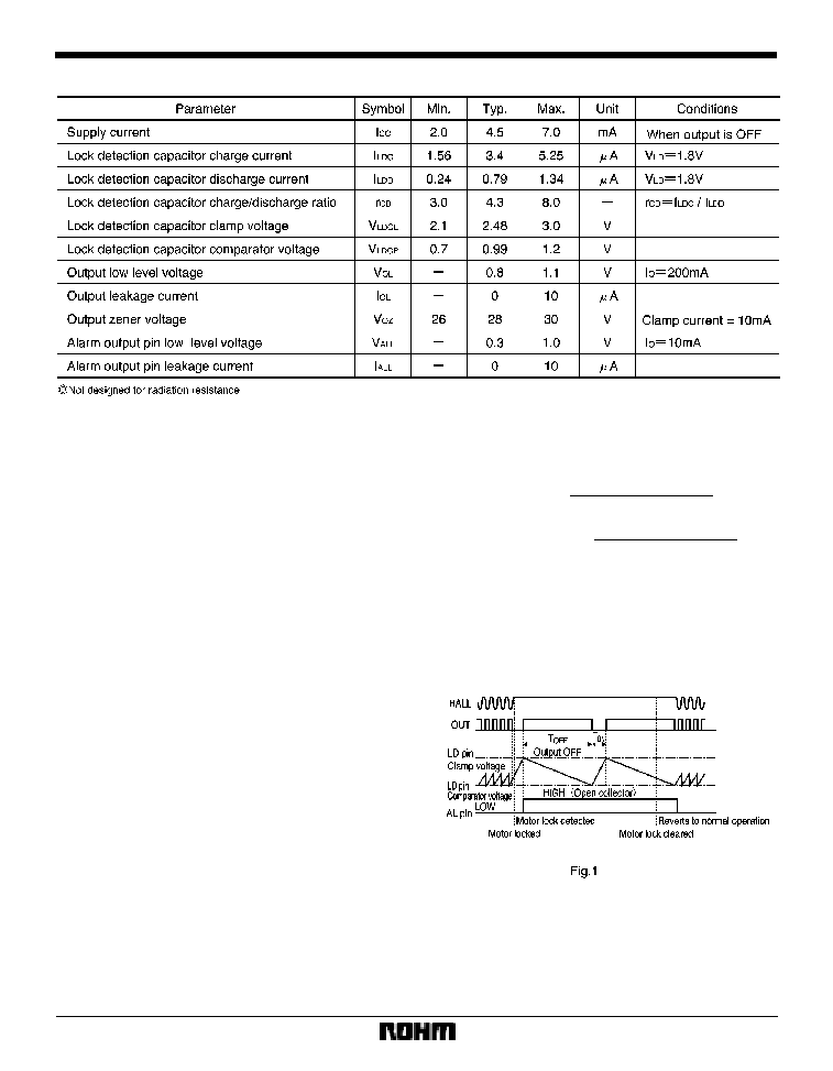
Electrical characteristics (unless otherwise noted, Ta = 25
_
C and V
CC
= 12V)
F
Lock detection
The automatic restart circuit detects a motor lock condi-
tion and automatically turns off the output current. When
the lock condition is cleared, the IC automatically restarts
and allow the motor to run.
In the BA6407AF, automatic restart is performed as fol-
lows.
A motor lock condition is detected when the Hall signal
stops switching.
The output is ON when the LD pin is being charged, and
OFF when the pin is being discharged.
S
The AL pin is ON during normal operation, and OFF
when the motor is locked.
S
The AL pin is an open collector output.
Output ON time (T
ON
) and OFF time (T
OFF
) determined by
the LD capacitor
where
C is the capacitance of the LD-pin external capacitor,
V
LDCL
is the LD-pin clamp voltage (2.48V),
V
LDCP
is the LD-pin comparator voltage (0.99V),
I
LDC
is the LD-pin charge current (3.4
�
A),
I
LDC
is the LD-pin discharge current (0.79
�
A).
I
LDC
T
ON
(Charge time)=
C
S
(V
LDCL
*
V
LDCP
)
I
LDD
T
OFF
(Discharge time)=
C
S
(V
LDCL
*
V
LDCP
)
(Typical value)

704
Motor driver ICs
BA6407AF
F
Operation notes
(1)
Thermal shutdown circuit
The IC has a built-in thermal shutdown circuit. There is
a temperature difference of 25
_
C (typical) between the
temperatures at which the circuit is activated and deacti-
vated.
(2)
Power dissipation
Power consumed in the IC can be calculated from the fol-
lowing equation :
P
C
=P
C1
)
P
C2
)
P
C3
P
C1
is power consumed by the supply current.
P
C1
=V
CC
I
CC
P
C2
is the output current consumption.
P
C2
=V
OL
I
O
V
OL
is the LOW level voltage of output pins 1 and 2.
P
C3
is power consumed by the AL pin.
P
C3
=V
ALL
I
AL
where V
ALL
is the AL-pin LOW level voltage and I
AL
is the
AL-pin sink current. Make sure that your application does
not exceed the allowable power dissipation of the IC.
(3)
Hall amplifier input voltage
The Hall current is given by:
where R
H
is the hall device impedance.
The R
1
and R
2
resistances must be set so as to maintain
the Hall amplifier input bias voltage within the range of 1V
to (V
CC
*
2V) including the signal amplitude. It is recom-
mended that the same value be used for both resistors
so that the Hall device output signal is centered around
V
CC
/ 2.
The Hall device may be affected by power supply noise
due to the PCB conductor pattern. If you have this prob-
lem, insert a capacitor C
1
as shown in Fig. 5.
If the conductor lines from the Hall device output termi-
nals to the Hall inputs of the IC are particularly long, noise
can be picked up and fed into the inputs. If you have this
problem, insert a capacitor C
2
as shown in Fig. 5. Note
that the Hall inputs have no hysteresis in this IC.
Fig.3
R
1
)
R
2
)
R
H
V
CC