
666
Motor driver ICs
3-phase motor driver
BA6870S
The BA6870S is a 3-phase, full-wave, pseudo-linear motor driver suited for VCR capstan motors. The IC has a torque
ripple cancellation circuit to reduce wow and flutter, and an output transistor saturation prevention circuit that provides
superb motor control over a wide range of current. The built-in motor power series regulator allows applications with low
power consumption.
F
Applications
3-phase VCR capstan motors
F
Features
1) 3-phase, full-wave, pseudo-linear driver system.
2) High performance torque ripple cancellation circuit.
3) Reversal braking by detecting the motor direction.
4) Saturation prevention circuit for high- and low-side
output transistors.
5) Motor power supply series regulators.
6) Built-in circuit for output-to-GND short-circuit detec-
tion.
F
Absolute maximum ratings (Ta = 25
_
C)
F
Recommended operating conditions (Ta = 25
_
C)

667
Motor driver ICs
BA6870S
F
Block diagram
668
Motor driver ICs
BA6870S
F
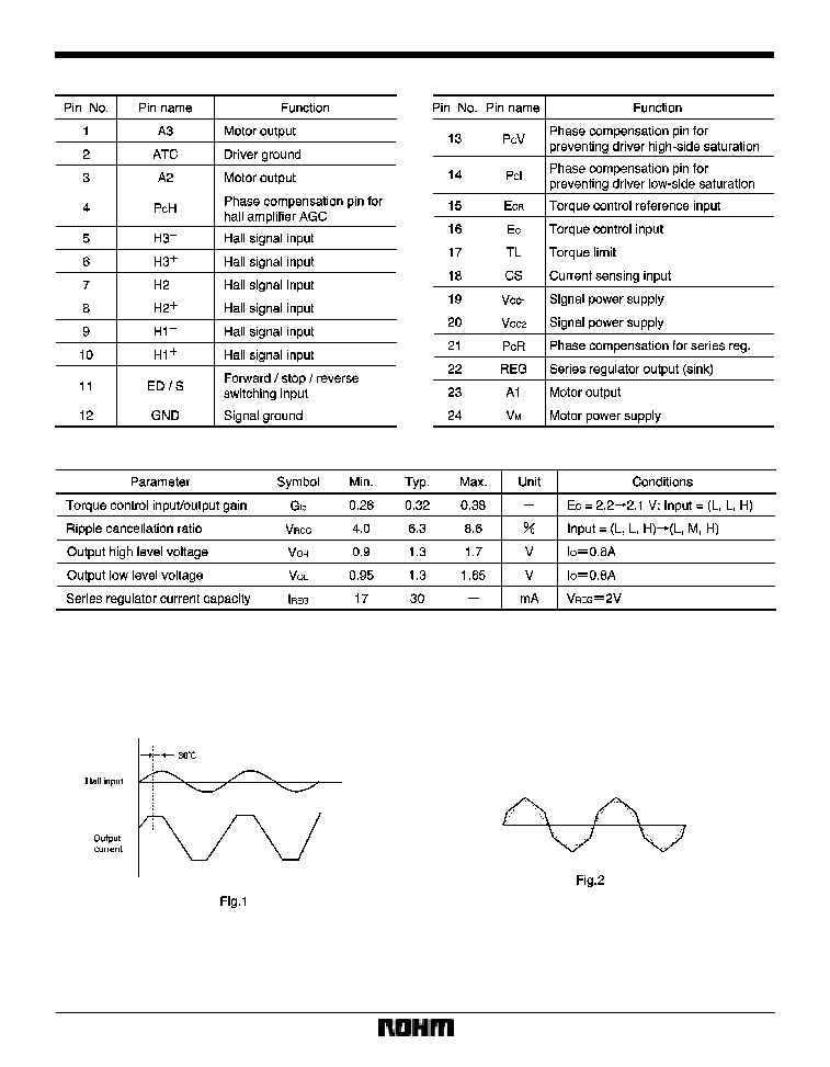
Pin descriptions
F
Electrical characteristics (unless otherwise noted, Ta = 25
_
C, V
CC
1 = 5V, V
M
= V
CC
2 = 12V)
F
Circuit operation
(1)
Pseudo-linear output and torque ripple cancellation
The IC generates a trapezoidal (pseudo-linear) output
current, whose waveform phase is 30 degrees ahead of
that of the Hall input voltage (Fig. 1).
The trapezoidal waveform of output current would create
intermittence in the magnetic field generated by the
3-phase motor, and would result in an irregular rotation
of the motor. To prevent this, the output waveform is ob-
tained by superimposing a triangular wave on the trape-
zoidal wave (Fig. 2). This process is called torque ripple
cancellation.

669
Motor driver ICs
BA6870S
(2)
Torque control and reversal brake
The output current can be controlled by adjusting the
voltage applied to the torque control pins (pins 15 and
16).
These pins are the inputs to a differential amplifier. A ref-
erence voltage between 2.3
X
3.0V (2.5V recommended)
is applied to pin 15.
A brake is applied to the motor as described in the follow-
ing. When the motor is running, pin 16 is given a negative
potential with respect to the reference potential. If the
pin-16 potential becomes positive, the IC detects the rise
of pin-16 potential above the reference potential and acti-
vates the motor direction detecting circuit.
The motor direction detecting circuit sends a signal to the
motor direction setting circuit to reverse the motor direc-
tion. This causes a braking torque that depends on the
pin-16 potential, so that the motor quickly reduces its
speed. At the same time, the positive pin-16 potential is
shifted to the reference potential, so that the motor stops
smoothly.
(3)
Output current sensing and torque limitation
Pin 2 is the ground pin for the output stage. To sense the
output current, a resistor (0.5
recommended) is con-
nected between pin 2 and the ground. The output current
is sensed by applying the voltage developed across this
resistor to pin 18 as a feedback.
The output current can be limited by adjusting the voltage
applied to pin 17. The current is limited when pin 17
reaches the same potential as pin 18. The output current
(I
Max.
) under this condition is given by:
Where R
2P
is the value of the resistor connected between
pin 2 and the ground, V
17P
is the voltage applied to pin 17,
and (TL
*
CS
ofs
) is the offset between the TL and CS pins.
(4)
Motor direction control (pin 11)
The motor mode is:
Forward when the pin 11 voltage is less than 0.9V,
Stop when the voltage is between 1.3
X
3.0V,
Reverse when the voltage is above 3.5V.
In the stop mode, high- and low-side output transistors
are turned off, resulting in a high impedance state.
(5)
Output transistor saturation prevention circuit
This circuit monitors the output voltage and maintain the
operation of the output transistors below their saturation
levels. Operating the transistors in the linear characteris-
tic range provides good control over a wide range of cur-
rent and good torque characteristics even during over-
loading.
R
2P
I
MAx.
=
V
17P
*
(TL
*
CS
ofs
)

670
Motor driver ICs
BA6870S
(6)
Series regulator
The BA6870S has a series regulator output pin. The IC
outputs a sink current according to the HIGH level output
voltage detected.
As shown in Fig. 7 the regulator circuit reduces the power
consumed by the IC by reducing the collector-to-emitter
(C-E) voltage of the driver transistors.
Nearly all the power dissipated by the IC is dissipated be-
tween the collectors and emitters of the output transis-
tors. More power is consumed as the C-E voltage in-
creases and as the output current increases.
The output transistor C-E voltage is equal to the differ-
ence between the supply voltage and the voltage applied
to the motor. Because the voltage across the motor de-
creases with decreasing drive current, the C-E voltage
must increase if the supply voltage is fixed.
Therefore, to improve the efficiency of the driver and to
prevent the power rating of the IC being exceeded, the
supply voltage must be varied in response to changes in
the output current. The supply voltage is decreased at
low current and increased at high current so that no ex-
cessive voltage is applied between the output transistor
collectors and emitters.
(7)
Output-to-ground short-circuit detection
The motor output pins of the IC may be short-circuited to
the ground by some fault conditions. A short-circuited
output can destroy the output transistors because of ex-
cessive current, excessive voltage, or both. Even when
a short-circuit condition does not completely destroy the
device, it can still cause extreme overheating. To prevent
this, the BA6870S contains a short-circuit detection cir-
cuit that turns off the motor drive current if the output-to-
ground potential becomes abnormally low.
F
Operation notes
The BA6870S has two thermal shutdown circuits (TSD1
and TSD2) to protect the IC. The typical shutdown tem-
peratures are 175
_
C for TSD1 and 215
_
C for TSD 2.
When the TSD1 is activated at an elevated chip tempera-
ture, the output pins (pins 1, 3, and 23) are set to the open
state. TSD1 is functional against excessive power dis-
sipation, output short-circuiting, and other irregularities in
the output current, but does not work against overheating
caused by high internal currents due to externally caused
IC damage or pin-to-pin short-circuiting.
When TSD2 is activated at a higher chip temperature, the
high- and low-side output transistors are turned on, and
the internal resistance between the motor power supply
pin (pin 24) and the output ground pin (pin 2) drops to less
than 3
. The motor power supply current (I
M
) is then giv-
en by
Where
I
M
is the motor supply current
V
M
is the motor supply voltage,
R
M
is the motor power supply output resistance,
R
2P
is the pin-2 resistance.
In your application, make sure to connect between the
motor power supply and pin 24 a circuit breaker that op-
erates at currents less than I
M
.
R
M
+R
2P
+3 (
)
I
M
=
V
M
(V)