 | –≠–ª–µ–∫—Ç—Ä–æ–Ω–Ω—ã–π –∫–æ–º–ø–æ–Ω–µ–Ω—Ç: BA7046F | –°–∫–∞—á–∞—Ç—å:  PDF PDF  ZIP ZIP |

1
Multimedia ICs
SYNC separator IC with AFC
BA7046 / BA7046F
The BA7046 and BA7046F separate the synchronization signals from a video signal and output the horizontal and
vertical synchronization signals (H
D
and V
D
), and the composite synchronization signal (Sync-out).
The H
D
and V
D
pulse phase difference is guaranteed.
∑
Applications
TVs and VCRs
∑
Features
1) Built-in AFC circuit.
2) H
D
and V
D
phase difference guaranteed.
3) Low power dissipation. (approx. 21mW)
4) Low external parts count.
5) 8-pin DIP / SOP package.
6) Horizontal free-run frequency does not require
adjustment.
∑
Absolute maximum ratings (Ta = 25∞C)
BA7046 (DIP)
BA7046F (SOP)
∑
Recommended operating conditions (Ta = 25∞C)
Parameter
Symbol
Unit
V
CC Max.
8.0
V
500
mV
Topr
∞
C
Tstg
∞
C
Pd
Limits
≠ 20 ~ + 75
≠ 55 ~ + 125
Power supply voltage
Power dissipation
Operating temperature
Storage temperature
Reduced by 5mW for each increase in Ta of 1
∞
C over 25
∞
C.
Parameter
Symbol
Unit
8.0
V
350
mW
Topr
∞
C
Tstg
∞
C
Pd
V
CC Max.
Limits
≠ 20 ~ + 75
≠ 55 ~ + 125
Power supply voltage
Power dissipation
Operating temperature
Storage temperature
When mounted on a 50mm
◊
50mm PCB board, reduced by 3.5mW for each increase in Ta of 1
∞
C
over 25
∞
C.
Parameter
Symbol
Min.
Typ.
Max.
Unit
V
CC
4.5
--
5.5
V
Operating power supply voltage

2
Multimedia ICs
BA7046 / BA7046F
∑
Input / output circuits
V
CC
1pin
1k
12k
100
µ
A
Fig. 1
200
V
CC
10k
4pin
Fig. 4
V
CC
100
6pin
10
µ
A
Fig. 5
8pin
V
CC
3k
3k
3k
3k
3k
3k
1k
Fig. 6
5k
V
CC
2pin
200
Fig. 2
3pin
200
Fig. 3
∑
Block diagrams
∑
Pin descriptions
1
2
3
4
8
7
6
5
H. OSC
V. SEPA
PHASE
COMP
SYNC
SEPA
1
2
3
4
5
6
7
8
Pin No.
Horizontal oscillator resistor
H
D
output
SYNC output (open collector)
V
D
output
GND
Video input
Power supply
Phase comparator output
Function

3
Multimedia ICs
BA7046 / BA7046F
∑
Electrical characteristics (unless otherwise noted Ta = 25∞C and V
CC
= 5.0V)
Parameter
Symbol Min.
Typ.
Max.
Unit
Conditions
I
Q
2.0
4.1
6.2
mA
--
0.08
0.15
--
0.1
0.3
V
4.7
4.9
--
V
13.9
15.7
17.5
kHz
±
2.1
±
2.9
--
kHz
T
HPH
≠ 1.0
0
+ 1.0
µ
s
pin2
pin≠ 6
T
HVD
17.0
23.5
30.0
µ
s
pin4
pin≠ 2
T
HD
4.6
5.1
5.6
µ
s
pin2
T
VD
190
230
270
µ
s
pin4
V
syn-Min.
V
P-L
V
P-H
f
H-O
V
P-P
f
CAP
pins 2, 4
Not designed for radiation resistance.
Quiescent current
Minimum synchronization separation level
Pulse voltage, LOW
Pulse voltage, HIGH
(Horizontal) free-running frequency
Capture range
Lock-in phase difference
H
D
, V
D
phase difference
H
D
pulse width
V
D
pulse width
pin 3 open
pin 6 terminated with 75
resistor
pins 2, 4
No input signal, I
1
= open
∑
Measurement circuit
8
7
6
5
1
2
3
4
I
I
100p
130k
V
T
V
T
V
T
1
µ
1
µ
75
Video In
+
+
+
A
47
µ
0.022
µ
39k
V
CC
2200p
470k
10k
V
CC
Fig. 7
∑
Circuit operation
(1) Synchronization separation circuit
Detects the charging current to a externally-connected
capacitor, and performs synchronization separation.
(2) Horizontal oscillation circuit
When a video signal is input, it is synchronized with
Hsync by the PLL. The horizontal free-running frequency
is determined by external resistor R1.
(3) Vertical synchronization separation circuit
When a video signal is input, synchronization signal
separation is done over the vertical synchronization
pulse interval.
f
H-O
= [kHz]
2.05E6
R
1
4
Multimedia ICs
BA7046 / BA7046F
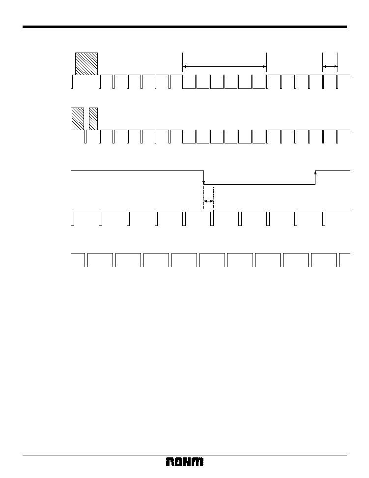
∑
V
IN
, H
D
and V
D
timing charts
1 / 2H
(OUT)
V
D
Fig. 8
NTSC signal
Odd field (IN)
NTSC signal
Even field (IN)
H
D
Odd field (OUT)
H
D
Even field (OUT)
(1) The rise and fall positions for V
D
are basically the same for both odd and even fields.
(2) H
D
shifts by 1 / 2H during the odd and even field interval.
(3) Only the odd field is given for the specification.
Vertical synchronization pulse interval
H
D
, V
D
phase difference

(1) Connect pin 1 to GND via a 120k
(approx.) resistor. Leave pins 2, 4 and 8 open.
(2) SYNC output polarity (pin 3) is positive.
(3) The delay time for rising edge of the SYNC output (pin 3) with respect to the falling edge of Sync for the Vsig
input signal (pin 6) is 850ns (reference value).
(4) The delay time for falling edge of the SYNC output (pin 3) with respect to the rising edge of Sync for the Vsig
input signal (pin 6) is 450ns (reference value).
∑
Attached components
Resistor R
1
should have a tolerance of ± 2%, and a temperature coefficient of 100ppm or lower.
5
Multimedia ICs
BA7046 / BA7046F
∑
Application example
8
8
7
6
5
R
2
470k
H. OSC
V. SEPA
PHASE
COMP
SYNC
SEPA
C
2
C
7
C
1
C
5
C
6
R
3
R
4
0.022
µ
47
µ
1
µ
1
µ
+
C
3
+
+
2200p
1000p
470k
330
10k
R
3
470k
R
2
Vsig
C
4
100p
R
1
130k
H
D
SYNC
V
D
10k
V
CC
= 5V
R
5
10k
1
2
3
4
V
CC
= 5V
C
3-1
0.47
µ
C
3-2
0.47
µ
C
2
2200p
V
CC
Fig.9
By configuring the circuit enclosed in the dotted line to that in the
diagram on the right, you can decrease the lock-in time and increase the
capture range.
8
7
6
5
H. OSC
V. SEPA
PHASE
COMP
SYNC
SEPA
C
7
C
1
C
5
C
6
R
4
V
CC
= 5V
V
CC
= 5V
0.022
µ
47
µ
1
µ
+
+
1000p
470k
330
Vsig
R
1
120k
H
D
SYNC
V
D
10k
R
5
1
2
3
4
Fig. 10
∑ When SYNC SEPA output only is used. H
D
and V
D
unused.
6
Multimedia ICs
BA7046 / BA7046F
∑
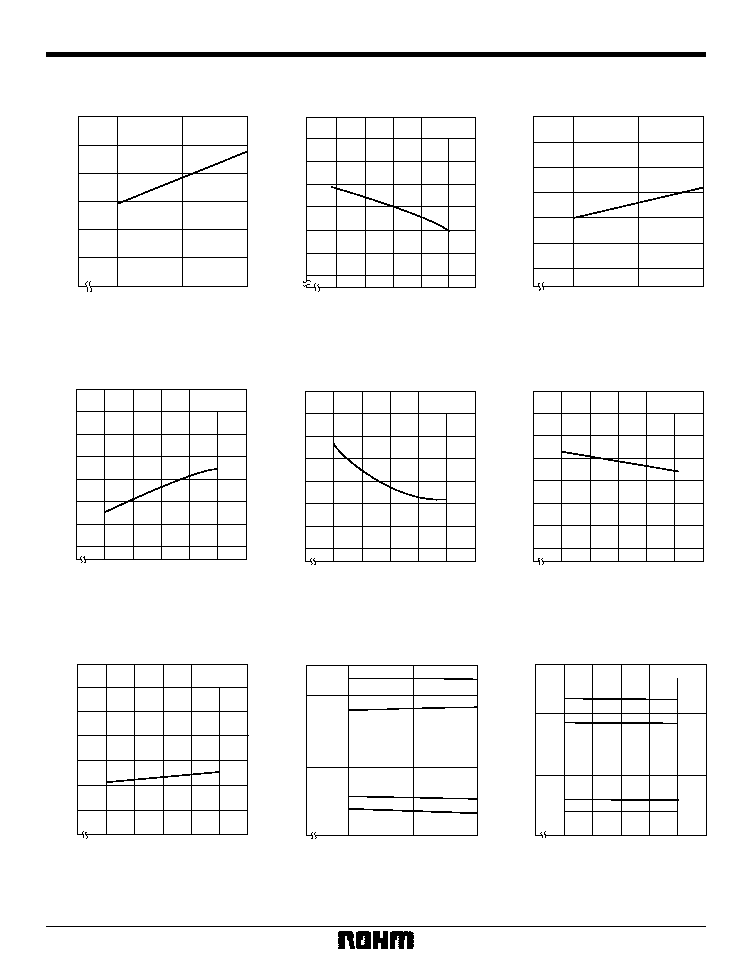
Electrical characteristic curves
H
D
∑ V
D
PULSE TIMING (
µ
s)
≠ 25
0
25
50
75
100
40
30
20
10
0
50
60
70
NTSC
V
CC
= 5.0V
TEMPERATURE (
∞
C)
Fig. 17 H
D
, V
D
phase difference vs.
temperature
FREQUENCY : f
(csp. lock)
(kHz)
POWER SUPPLY VOLTAGE (V)
20
15
10
4.5
5.0
5.5
+ lock
+ cap
≠ lock
≠ cap
Fig. 18 Capture range / lock range vs.
power supply voltage
FREQUENCY : f
(csp.lock)
(kHz)
TEMPERATURE (
∞
C)
≠ 25
0
25
50
75
100
V
CC
= 5.0V
+ lock
+ cap
≠ lock
≠ cap
20
15
10
Fig. 19 Capture range charging / lock
range vs. temperature
HORIZONTAL FREQUENCY : f (kHz)
TEMPERATURE (
∞
C)
15.2
V
CC
= 5.0V
15.4
15.6
15.8
16.0
16.2
16.4
16.6
≠ 25
0
25
50
75
100
Fig. 14 Horizontal free-running
frequency vs. temperature
H
D
PULSE WIDTH : H
D
(
µ
s)
TEMPERATURE (
∞
C)
NTSC
V
CC
= 5.0V
4.4
4.6
4.8
5.0
5.2
5.4
5.6
5.8
≠ 25
0
25
50
75
100
Fig. 15 H
D
pulse width vs.
temperature
V
D
PULSE WIDTH : V
D
(
µ
s)
TEMPERATURE (
∞
C)
NTSC
V
CC
= 5.0V
≠ 25
0
25
50
75
100
180
190
200
210
220
230
240
250
Fig. 16 V
D
pulse width vs.
temperature
CURRENT : I
CC
(mA)
POWER SUPPLY VOLTAGE (V)
6
5
4
3
2
1
0
4.0
5.0
6.0
Fig. 11 Quiescent current vs.
power supply voltage
CURRENT : I
CC
(mA)
TEMPERATURE (
∞
C)
6.0
5.5
4.5
4.0
5.0
3.0
2.5
3.5
≠ 25
0
25
50
75
100
V
CC
= 5.0V
Fig. 12 Quiescent current vs.
temperature
HORIZONTAL FREQUENCY : f (kHz)
POWER SUPPLY VOLTAGE (V)
16.4
16.2
16.0
15.8
15.6
15.4
15.2
4.5
5.0
5.5
Fig. 13 Horizontal free-running frequency
vs. power supply voltage
7
Multimedia ICs
BA7046 / BA7046F
∑
Operation notes
∑ Make the ground line as thick as possible.
∑ Keep power supply noise to a minimum.
∑
External dimensions (Units: mm)
SIGNAL - LOCK IN TIME (ms)
FREQUENCY (kHz)
13
14
15
16
17
18
19
20
300
200
100
0
V
CC
= 5.0V
f
LOCK
= 15.734kHz
Fig. 20 Time from no signal
to pull in
POWER LOCK IN TIME (ms)
FREQUENCY (kHz)
13
14
15
16
17
18
20
700
600
500
400
300
200
100
0
V
CC
= 5.0V
f
LOCK
= 15.734kHz
19
Fig. 21 Time from power
on to pull in
BA7046
BA7046F
DIP8
SOP8
0.5
±
0.1
3.2
±
0.2
3.4
±
0.3
8
5
1
4
9.3
±
0.3
6.5
±
0.3
0.3
±
0.1
0.51Min.
2.54
0
∞
~ 15
∞
7.62
0.4
±
0.1
1.27
0.15
0.3Min.
0.15
±
0.1
0.11
6.2
±
0.3
4.4
±
0.2
5.0
±
0.2
8
5
4
1
1.5
±
0.1