 | ÐлекÑÑоннÑй компоненÑ: BA7232 | СкаÑаÑÑ:  PDF PDF  ZIP ZIP |
Äîêóìåíòàöèÿ è îïèñàíèÿ www.docs.chipfind.ru
1
Multimedia ICs
Color TV Signal Encoder
BA7232FS
The BA7232FS converts analog RGB signals into color TV signals in the NTSC and PAL formats. From inputs of
analog RGB signals, a composite synch signal, burst pulses and a color carrier, this IC generates a color TV signal,
and can be adapted for either NTSC or PAL standards, which are selected externally. When set to PAL, the
BA7232FS changes chroma phase according to the burst flag pulses.
The chroma signals and luminosity signals can be combined into a color TV signal or output separately, making this
IC suitable for S pins. Also, this IC comes with an output pin for the analog RGB signal. Each output has a built-in
75
driver.
·
Applications
TV peripherals
·
Features
1) Can be adapted for NTSC and PAL formats.
2) Internal flip-flop for PAL phase switching.
3) Separate Y / C output pins.
4) Analog RGB signal output pins.
5) Internal 75
driver. (outputs color TV signals, lumi-
nosity signals, chroma signals and analog RGB sig-
nals)
6) Adaptable for color subcarrier pulse input.
·
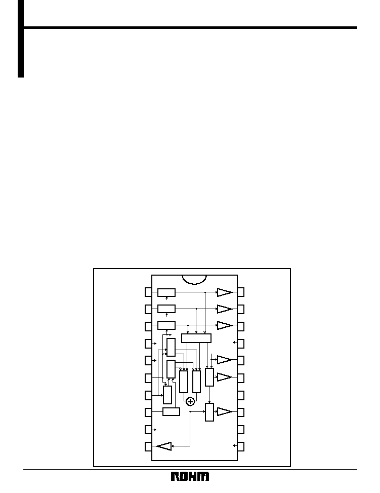
Block diagram
1
BIN
2
GIN
3
RIN
4
V
CC
1
5
SYNCIN
6
BFPIN
7
NT / PAL
8
SCIN
9
GND1
10
COUT
20
BOUT
19
GOUT
18
ROUT
17
V
CC
2
16
SYNCOUT
15
YOUT
14
N.C.
13
VOUT
12
N.C.
11
GND2
GND
GND
FILTER
F · F
Y / C MIX
SYNC
MIX
PHASE
GEN.
BURST
GEN.
SYNC
V
CC
V
CC
B - Y MOD.
R - Y MOD.
BFP
BFP
BFP
MATRIX
SYNC
75
75
75
75
75
75
CLAMP
CLAMP
CLAMP
2
Multimedia ICs
BA7232FS
·
Pin descriptions
Pin name
1
BIN
Analog B signal input
2
GIN
Analog G signal input
3
RIN
Analog R signal input
4
5
SYNCIN
6
BFPIN
7
NT / PAL
8
SCIN
Color subcarrier input
9
GND1
Ground for all drivers other than the 75
driver
10
COUT
Chroma signal output. Internal 75
driver.
11
GND2
Ground for the 75
driver
12
N.C.
This pin is not connected inside the IC.
13
VOUT
Color TV signal output. Internal 75
driver.
14
N.C.
This pin is not connected inside the IC.
15
YOUT
Luminance signal output. Internal 75
driver.
16
SYNCOUT
Composite synchronization signal output
17
18
ROUT
Analog R signal output. Internal 75
driver
19
GOUT
Analog G signal output. Internal 75
driver.
20
BOUT
Analog B signal output. Internal 75
driver.
Pin No.
Function
V
CC
2
Power supply pin for all drivers other than the 75
driver
Burst flag pulse input (negative logic)
Composite synchronization signal input (negative logic)
Power supply pin for all drivers other than the 75
driver
Selecting the type of color TV signal output
(high = NTSC, low = PAL)
V
CC
1
·
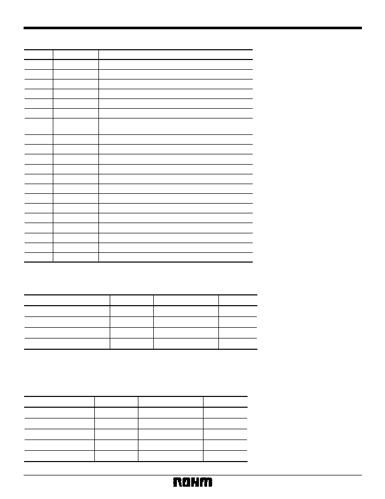
Absolute maximum ratings (Ta = 25°C)
·
Recommended operating conditions (Ta = 25°C)
Parameter
Symbol
Limits
Unit
Power supply voltage
V
CC
7
V
Power dissipation
Pd
mW
Operating temperature
Topr
°
C
Storage temperature
Tstg
°
C
750
Reduced by 7.5mW for each increase in Ta of 1
°
C over 25
°
C.
When mounted on a 70
×
70
×
1.6mm glass epoxy board.
20 ~ + 70
55 ~ + 125
Parameter
Symbol
Limits
Unit
Power supply voltage
V
CC
4.5 ~ 5.5
V
RIN input level
RI
0 ~ 0.7
V
P-P
GIN input level
GI
0 ~ 0.7
V
P-P
BIN input level
BI
0 ~ 0.7
V
P-P
SCIN input level
SC
0.45 ~ 0.6
V
P-P
3
Multimedia ICs
BA7232FS
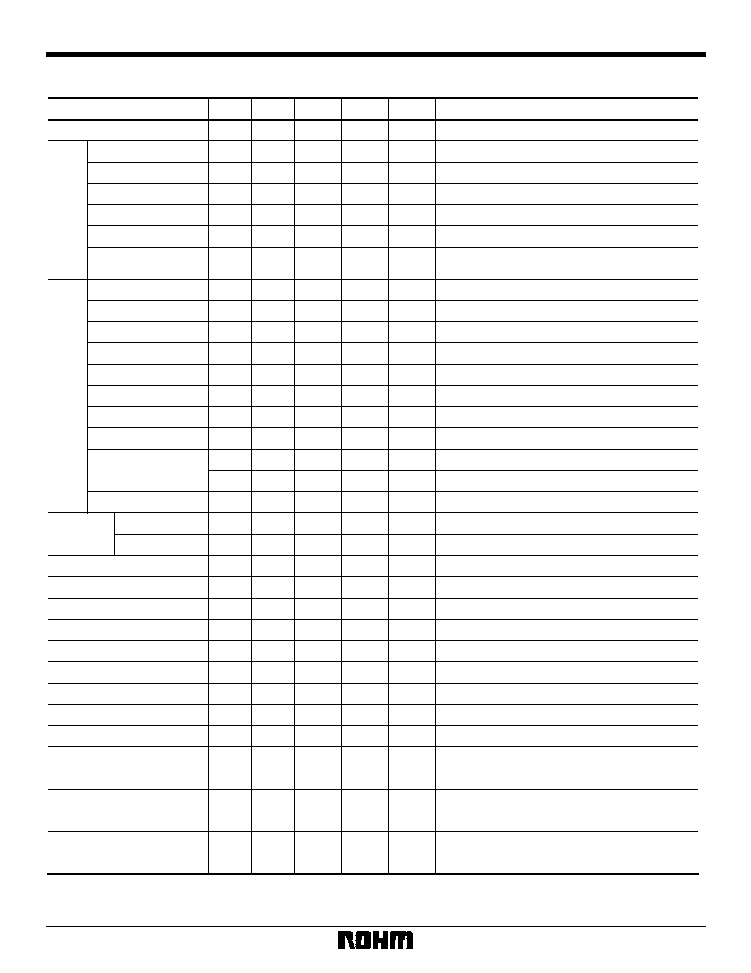
·
Electrical characteristics (unless otherwise noted, Ta = 25°C, V
CC
= 5V, XTAL = 3.58MHz)
V
IL
--
--
0.8
V
V
IH
2.2
--
--
V
Input impedance
Z
I
8
13.5
--
k
Parameter
Symbol
Min.
Typ.
Max.
Unit
Conditions
Current dissipation
I
CC
33.0
48.0
63.0
mA
YOUT
VOUT
Luminance level
L
0.63
0.70
0.77
V
P-P
RI
=
GI
=
BI
= 0.7V
P-P
Luminance level R
L(R)
0.19
0.21
0.23
V
P-P
Luminance level G
L(G)
0.37
0.41
0.45
V
P-P
Luminance level B
L(B)
0.07
0.08
0.09
V
P-P
Synchronization level
S
0.27
0.30
0.33
V
P-P
R
S/L
0.38
0.43
0.48
R
YO
=
S
/
L
COUT
VOUT
R / burst level ratio
R
R/BU
2.84
3.16
3.48
G / burst level ratio
R
G/BU
2.65
2.95
3.25
B / burst level ratio
R
B/BU
2.01
2.24
2.47
R phase
R
94
104
114
deg
G phase
G
231
241
251
deg
B phase
B
337
347
357
deg
Burst level
BU
0.26
0.29
0.32
V
P-P
Carrier leak
CL
--
--
--
--
--
--
--
--
--
--
--
--
--
--
--
--
--
--
--
--
35
mV
P-P
PAL burst phase
BU
+
125
135
145
deg
BU
215
225
235
deg
PAL burst level ratio
R
BU
0.9
1.0
1.1
SYNCOUT
2.00
2.50
5.00
V
0
--
--
--
0.40
V
RO
0.63
0.70
0.77
V
P-P
RI
= 0.7V
P-P
GO
0.63
0.70
0.77
V
P-P
GI
= 0.7V
P-P
BO
0.63
0.70
0.77
V
P-P
BI
= 0.7V
P-P
V
YO
1.60
2.00
2.40
V
V
CO
2.20
2.60
3.00
V
V
VO
1.75
2.15
V
V
RO
1.25
1.65
2.05
V
V
GO
1.25
1.65
2.05
V
V
BO
1.25
1.65
2.05
V
Synchronization /
luminance level ratio
Input voltage "L" level
Input voltage "H" level
SYNC, BFP, NT / PAL
SYNC, BFP, NT / PAL
SYNC, BFP, NT / PAL
1.35
YOUT DC voltage
COUT DC voltage
VOUT DC voltage
ROUT DC voltage
GOUT DC voltage
BOUT DC voltage
Output level (HIGH)
Output level (LOW)
ROUT
GOUT
BOUT
output level
output level
output level
RI
= 0.7V
P-P
1
GI
= 0.7V
P-P
1
BI
= 0.7V
P-P
1
RI
= 0.7V
P-P
1
GI
= 0.7V
P-P
1
BI
= 0.7V
P-P
1
SW1 = 2
1
SW1 = 2
1
SW1 = 2
1
1 Guaranteed performance.
2 Measured 3.5
µ
s after burst with a 3.58 MHz BPF.
3 Measured with a 3.58 MHz BPF.
Not designed for radiation resistance.
1
1
1
3
2
4
Multimedia ICs
BA7232FS
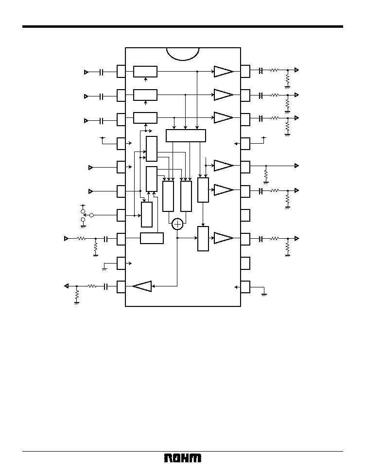
·
Measurement circuit
1
2
3
4
5
6
7
8
9
10
20
19
18
17
16
15
14
13
12
11
GND
GND
FILTER
F · F
Y / C
MIX
SYNC
MIX
PHASE
GEN.
BURST
GEN.
SYNC
V
CC
V
CC
B - Y MOD.
R - Y MOD.
BFP
BFP
BFP
MATRIX
SYNC
CLAMP
CLAMP
CLAMP
0.47
µ
0.1
µ
75
75
COUT
measurement point
560
4.7k
Color subcarrier
V
CC
Burst flag pulse
(BFP)
Composite synch
V
CC
0.1
µ
0.1
µ
0.1
µ
RIN input
GIN input
BIN input
75
75
220
µ
+
BOUT
measurement point
75
75
220
µ
+
GOUT
measurement point
75
75
220
µ
+
ROUT
measurement point
75
75
2K
220
µ
+
YOUT
measurement point
75
75
220
µ
+
VOUT
measurement point
V
CC
SYNCOUT
measurement point
SW1
1
2
75
75
75
75
75
75
5
Multimedia ICs
BA7232FS
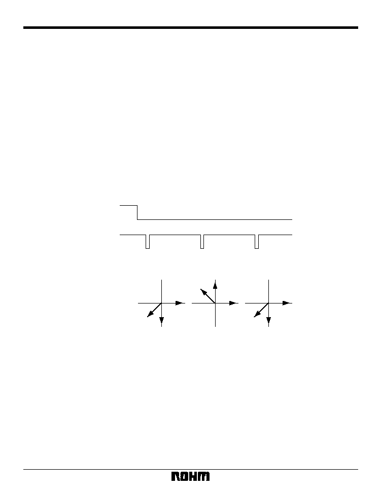
NT / PAL
BFP
Chroma phases
burst
B - Y
R - Y
burst
burst
B - Y
B - Y
R - Y
R - Y
·
Circuit operation
(1) SYNCIN is for composite synch input. During low
input, the synchronization signal is output to YOUT,
VOUT and SYNCOUT.
(2) BFP is for burst flag pulse input. During low input,
the burst signal is output to pins CO and VO. When the
IC is set to PAL, it is this signal that directs the phase
inversion of the chroma signals. This signal also con-
trols the timing of the pedestal clamps of RIN, GIN and
BIN. During low input, the pedestal levels of RIN, GIN
and BIN are kept constant by charging an attached
capacitor.
(3) NT / PAL is the NTSC / PAL selector pin, and con-
nects to V
CC
when set to NTSC and to GND when set
to PAL.
(4) SCIN is for color subcarrier input. Set input to a
pulse wave or sine wave (3.579545MHz for NTSC and
4.433619MHz for PAL).
(5) COUT and YOUT are for output of chroma signals
and luminosity signals, respectively. Because the chro-
ma signal and luminosity signals can be output sepa-
rately, the IC can be adapted for S pins. Each has a
75
driver.
(6) VOUT is for color TV signal output, and has an
internal 75
driver.
(7) ROUT, GOUT and BOUT are for analog RGB sig-
nal output, and have an internal 75
driver.
The relationship between chroma phase and burst phase during PAL processing is as follows.