
1
Multimedia ICs
Dual Voltage-controlled Amplifier
BA7655A / BA7655AF
The BA7655A and BA7655AF are dual voltage-controlled amplifier ICs designed for use in camcorders and VCRs.
By varying the control voltage the amplifier gain can varied from -6dB to +6dB. When the control pin voltage drops
below 1V the amplifier enters Power Save Mode which mutes the output and reduces the current drawn by the IC.
∑
Applications
Video cassette recorders and camcorders
∑
Features
1) Wide bandwidth.
2) Wide dynamic range.
3) Low power cousumption.
4) Output muting possible.
5) Low voltage gain temperature drift.
∑
Block diagram
VCA2
VCA1
GND
OUT1
CTL1
IN1
IN2
CTL2
OUT2
5
6
7
8
1
2
3
4
V
CC

2
Multimedia ICs
BA7655A / BA7655AF
∑
Pin descriptions
Pin name
1
IN1
Input 1
2
CTL1
Control 1
3
OUT1
Output 1
4
GND
GND
5
OUT2
Output 2
6
CTL2
Control 2
7
IN2
Input 2
8
V
CC
Power supply
Pin No.
Function
∑
Input circuits
2, 6
1, 7
3, 5
V
CC
V
CC
40k
40k
V
CC
(Typ.)
(Typ.)
3.0V (Typ.)
1m (Typ.)
2.5V
(Typ.)
∑
Absolute maximum ratings
Parameter
Symbol
Unit
Power supply voltage
V
CCMax.
8.0
V
Power dissipation
Pd
500 (BA7655A : DIP8)
1
350 (BA7655AF : SOP8)
2
mW
Operating temperature
Topr
∞
C
Storage temperature
Tstg
∞
C
≠ 20 ~ + 80
≠ 55 ~ + 125
1 Reduced by 5.0mW for each increase in Ta of 1
∞
C over 25
∞
C.
2 Reduce by 3.5mW for each increase in Ta of 1
∞
C over 25
∞
C, when mounted on a 50mm
◊
50mm.
Limits
∑
Recommended operating conditions (Ta = 25∞C)
Parameter
Symbol
Limits
Unit
Power supply voltage
V
CC
4.5 ~ 5.5
V

3
Multimedia ICs
BA7655A / BA7655AF
∑
Electrical characteristics (unless otherwise noted , Ta = 25∞C , V
CC
= 5.0V)
Not designed for radiation resistance.
Items marked with an asterisk are rerference values.
Parameter
Symbol
Min.
Typ.
Max.
Unit
Voltage
Conditions
Supply current
One channel
ICC1
--
4.6
7.0
mA
3.0
Set control voltage to 1V or less,
when only one channel is used.
Both channels
ICC2
--
7.8
12.0
Maximum output voltage
VMax.
2.5
2.8
--
V
P-P
5.0
Frequency characteristics
Gf
≠ 1.0
0.0
dB
3.0
Minimum voltage gain
GVMin. ≠ 8.0
≠ 6.0
≠ 4.0
dB
2.0
f = 1MHz
Maximum voltage gain
GVMax.
4.0
6.0
8.0
dB
5.0
f = 1MHz
Secondary harmonic distortion
2HD
--
≠ 40
--
dB
3.0
Audio distortion
AD
--
1.0
--
%
3.0
Muting output voltage
VMUTE
--
--
100
mV
1.0
Set control voltage to 1 V or less
V S / N
--
≠ 60
--
dB
3.0
A S / N
--
≠ 60
--
dB
3.0
Audio
S / N
Video
S / N
1.0
f = 1kHz, THD = 1%
f = 13MHz / 1MHz, V
IN
= 0.5V
P-P
f = 5.0M, V
IN
= 1V
P-P
f = 1kHz, V
IN
= 1V
P-P
∑
Circuit operation
0 0.5 1 1.5 2 2.5 3 3.5 4 4.5 5
POWER SAVE MODE
8
6
4
2
0
≠ 2
≠ 4
≠ 6
≠ 8
≠ 10
≠ 12
≠ 14
Control voltage (V)
GAIN (dB)
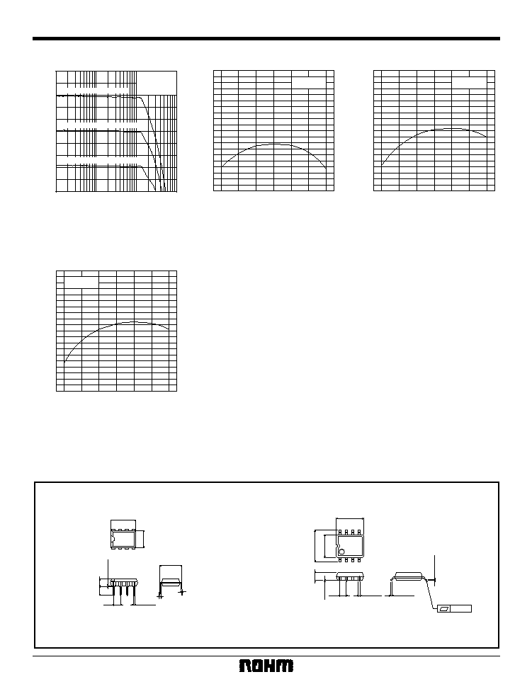
Fig. 1 Voltage gain vs.
control voltage characteristics
The gain of a VCA (voltage-controlled amplifier) can be
varied by an external control voltage. By varying the
control voltage from 2V to 5V (in the case of a 5V
power supply), the gain of the amplifiers in this IC can
be varied over the range -6dB to +6dB (see Figs. 1
and 2 below).
When only one of the two amplifiers is being used, by
setting the voltage on the CTL pin of the unused ampli-
fier to 1V or less, it can be put into Power Save Mode.
In Power Save Mode, the circuit current for the IC is
cut by 40%, and the output is muted.
VCA
IN
OUT
Control voltage
Fig. 2
CTL Voltage
Status
2V ~ 5V
Variable gain
1V or less
Power save
4
Multimedia ICs
BA7655A / BA7655AF
∑
Electrical characteristic curves
1M
10M
100M
10.0
8.0
6.0
4.0
2.0
0.0
100K
≠ 2.0
≠ 4.0
≠ 6.0
≠ 10.0
≠ 8.0
CONTROL VOLTAGE = 5V
CONTROL VOLTAGE = 3V
CONTROL VOLTAGE = 2V
VOLTAGE GAIN : V
G
(dB)
V
CC
= 5V
V
IN
= 0.5V
P-P
FREQUENCY :
f (Hz)
Fig. 3 Voltage gain vs.
frequency
7
6.5
6
5.5
5
0
25
50
75
100
≠ 25
≠ 50
Max. VOLTAGE GAIN (dB)
AMBIENT TEMPERATURE : Ta (
∞
C)
V
CC
= 5V
Fig. 4 Maximum voltage gain vs.
ambient temperature
1
0.5
0
0
25
50
75
100
≠ 0.5
≠ 1
≠ 50
≠ 25
Typ. VOLTAGE GAIN (dB)
AMBIENT TEMPERATURE : Ta (
∞
C)
V
CC
= 5V
Fig. 5 Voltage gain vs.
temperature
0
25
50
75
100
≠ 5
≠ 5.5
≠ 6
≠ 6.5
≠ 7
≠ 50
≠ 25
Min. VOLTAGE GAIN (dB)
AMBIENT TEMPERATURE : Ta (
∞
C)
V
CC
= 5V
Fig. 6 Minimum voltage gain vs.
temperature
∑
External dimensions (Units: mm)
BA7655A
BA7655AF
DIP8
SOP8
0.5
±
0.1
3.2
±
0.2
3.4
±
0.3
8
5
1
4
9.3
±
0.3
6.5
±
0.3
0.3
±
0.1
0.51Min.
2.54
0
∞
~ 15
∞
7.62
0.4
±
0.1
1.27
0.15
0.3Min.
0.15
±
0.1
0.11
6.2
±
0.3
4.4
±
0.2
5.0
±
0.2
8
5
4
1
1.5
±
0.1