 | –≠–ª–µ–∫—Ç—Ä–æ–Ω–Ω—ã–π –∫–æ–º–ø–æ–Ω–µ–Ω—Ç: BA7665FS | –°–∫–∞—á–∞—Ç—å:  PDF PDF  ZIP ZIP |
1
Multimedia ICs
3-channel 75
driver with Y / C MIX
BA7665FS
The BA7665FS has three 75
driver circuits with 6dB amplifiers, and includes a Y / C MIX circuit. The IC can pro-
vide a 75
drive with a composite Y signal, C signal, or a Y / C MIX signal. Dual-circuit drive capacity for each load
is provided, and a sag compensation function is provided to allow use of smaller coupling capacitors.
The composite Y signal input is a sync-tip clamp input, and the chroma input is a biased input.
The three channels can be simultaneously muted, or the chroma signal only (in the case of C / Y output, only Y is
output), and output short circuit protection and power save circuits are also provided.
∑
Applications
Digital AV equipment, DVD and DVC players
∑
Features
1) Y / C MIX circuit.
2) Low power consumption (typ. 130mW).
3) Output mute circuit.
4) Power save circuit.
5) Output protection circuit.
6) Sag compensation circuit allows small output cou-
pling capacitors.
7) Two-circuit drive possible for loads.
8) Compact SSOP-A 16-pin package.
∑
Absolute maximum ratings (Ta = 25∞C)
Parameter
Symbol
Limits
Unit
Power supply voltage
Power dissipation
Operating temperature
Storage temperature
V
CC
Pd
Topr
Tstg
8
650
≠ 25 ~ + 75
≠ 55 ~ + 125
V
mW
∞
C
∞
C
Reduced by 6.5mW for each increase in Ta of 1
∞
C over 25
∞
C.
∑
Recommended operating conditions (Ta = 25∞C)
Parameter
Symbol
Unit
Max.
Typ.
Min.
Power supply voltage
V
CC
4.5
5.5
5.0
V
Not designed for radiation resistance.
2
Multimedia ICs
BA7665FS
∑
Electrical characteristics (unless otherwise noted, Ta = 25∞C, V
CC
= 5V)
Parameter
Symbol
Min.
Typ.
Max.
Unit
Conditions
Circuit current
Maximum output level
Frequency characteristics
Inter channel crosstalk
Mute attenuation
Mute switch high level
Mute switch low level
Input impedance
I
CC
V
om
G
f
C
T
M
T
V
THH
V
THL
Z
IN
13.0
2.6
≠ 1.0
--
--
2.5
0
16
26.0
3.0
0.0
≠ 60
≠ 60
--
--
20
39.0
--
1.0
--
--
V
CC
1.0
24
mA
V
P-P
dB
dB
dB
V
V
k
No signal
f = 1kHz, THD = 1 %
f = 7MHz / 1MHz, 1V
P-P
f = 4.43MHz, 1V
P-P
f = 4.43MHz, 1V
P-P
Chroma input pin (pin 7)
∑
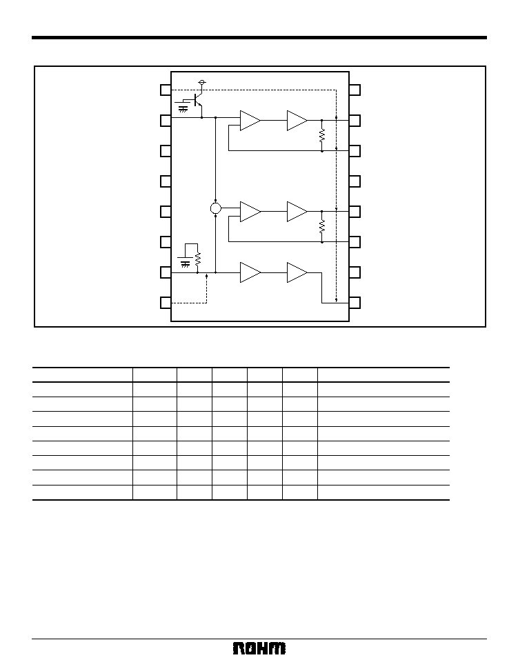
Block diagram
+
6dB
Mute
75
6dB
75
6dB
75
20k
1
2
3
4
5
6
7
8
MUTEA
INA
GND
GND
GND
N.C.
INB
MUTEB
16
15
14
13
12
11
10
9
V
CC
1
OUTA1
OUTA2
V
CC
2
MIXOUT1
MIXOUT2
N.C.
OUTB
Chroma Mute
3
Multimedia ICs
BA7665FS
∑
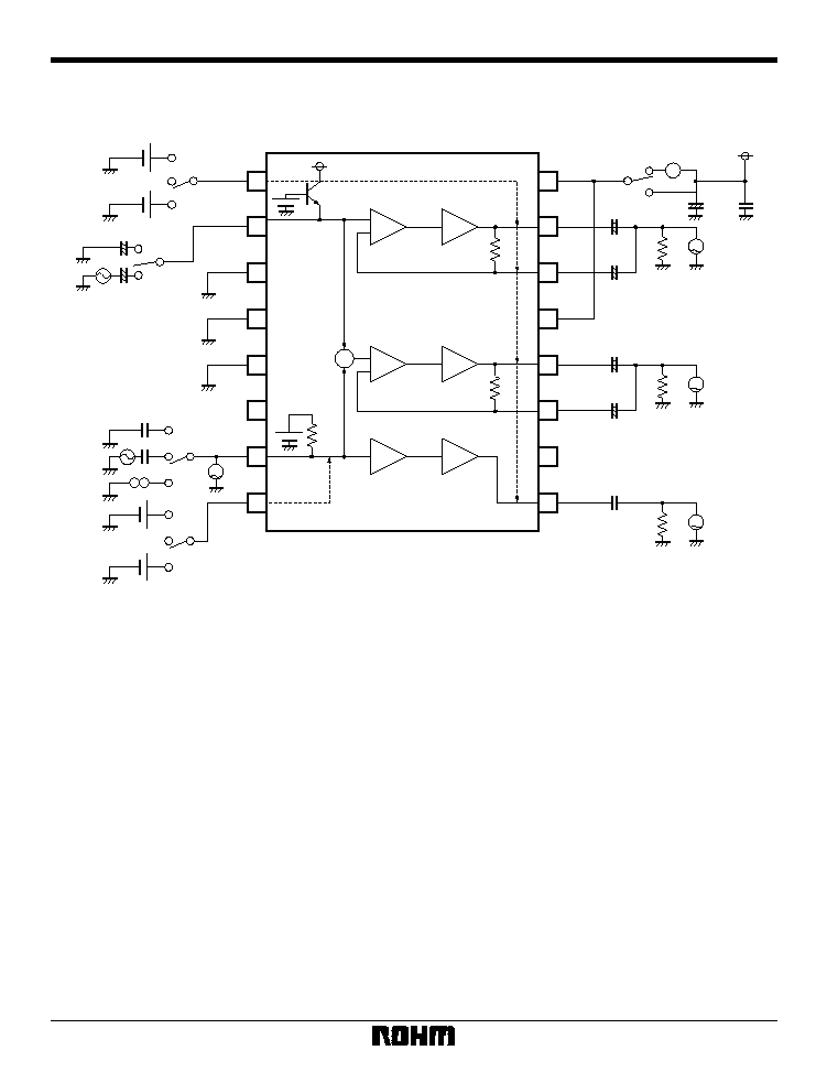
Measurement circuit
+
6dB
Mute
75
6dB
75
6dB
75
N.C.
N.C.
20k
+
+
+
100
µ
F
22
µ
F
0.1
µ
F
47
µ
F
1
3.3V
1.2V
2
3
4
5
6
7
8
16
15
14
13
12
11
10
9
Chroma Mute
A
V
+
+
100
µ
F
22
µ
F
V
0.1
µ
F
V
SW16
1
2
75
75
75
1
1
2
2
3
SW1
SW2
+
1
µ
F
+
1
µ
F
1
2
3
1
2
3
0.1
µ
F
0.1
µ
F
3.3V
1.2V
SW7
SW8
V
Fig.1

4
Multimedia ICs
BA7665FS
∑
Measurement conditions
Parameter
Symbol
Measurement
method
Switch conditions
Circuit current
Maximum
output level
Frequency
characteristics
Crosstalk
Mute attenuation
Chroma mute attenuation
Input impedance
Voltage gain
Inter-channel
voltage gain differential
I
CC
V
OM1
V
OM2
V
OM3
G
F1
G
F2
G
F3
G
T1
G
T2
M
T1
M
T2
M
T3
M
TC1
M
TC2
Z
IN
G
V1
G
V2
G
V3
G
VC
OUTA
MIXOUT
OUTB
OUTA
MIXOUT
OUTB
OUTB
OUTA
OUTA
OUTB
OUTA
MIXOUT
OUTB
MIXOUT
OUTB
OUTA
MIXOUT
OUTB
Note 1
Note 2
Note 3
Note 4
Note 5
Note 5
Note 6
Note 7
Note 8
SW
1
2
3
3
3
3
3
3
3
3
1
1
1
3
3
3
3
3
3
--
SW
2
1
2
2
1
2
2
1
1
2
2
2
1
1
1
1
2
2
1
--
SW
7
1
1
1
2
1
1
2
2
1
1
1
2
2
2
3
1
1
2
--
SW
8
2
3
3
3
3
3
3
3
3
3
3
3
1
1
3
3
3
3
--
SW
16
1
2
2
2
2
2
2
2
2
2
2
2
2
2
2
2
2
2
--
The mute switch level was substituted by using H = 2.4V and L = 1.1V for the above measurements.
--
--
Measurement method
Note 1: Measure the quiescent current.
Note 2: Connect a distortion meter to the output, and input a f = 1kHz sine wave.
Adjust the output level until the output distortion is 1%. The output voltage at this time is the maximum output level V
OM
[V
P-P
].
Note 3: Input 1V
P-P
, 7MHz and 1MHz sine waves, and measure the corresponding outputs V
O7
and V
O1
. The frequency characteristic is given by
G
F
= 20
Log (V
O7
/ V
O1
) [dB].
Note 4: Input a 1V
P-P
, 4.43MHz sine wave, and measure the output Vo [V
P-P
] The interchannel crosstalk is given by C
T
= 20
Log (V
O
/ V
IN
) [dB].
Note 5: Input a 1V
P-P
, 4.43MHz sine wave, and measure the output Vo [V
P-P
] The mute attenuation is given by
M
T
= 20
Log (V
O
/ V
IN
) [dB].
Note 6: Measure the input pin voltage V
IN
50 when a current of DC50
µ
A is flowing into the input pin. Measure the input pin open-circuit voltage.
The input impedance is given by
Z
IN
= | V
IN50
≠ V
IN0
| / 50
10
3
[k
].
Note 7: Input a 1V
P-P
, 4.43MHz sine wave, and measure the output V
O
[V
P-P
] The voltage gain is given by
Gv = 20
log (V
O
/ V
IN
) [dB].
Note 8:
G
VC
= | G
V1
≠ G
V2
| [dB]
5
Multimedia ICs
BA7665FS
Parameter
Symbol
Min.
Typ.
Max.
Unit
Conditions
Voltage gain
Interchannel voltage gain
G
v
G
v
5.5
≠ 0.5
6.0
0.0
6.5
0.5
dB
dB
f = 4.43MHz, 1V
P-P
f = 100kHz, 1V
P-P
∑
Guaranteed design values (unless otherwise noted, Ta = 25∞C, V
CC
= 5V)
∑
Mute SW mode settings
3ch MUTE
∑ MUTEA (1pin)
H
NORMAL
L
CHROMA MUTE
∑ MUTEB (8pin)
H
NORMAL
L
∑
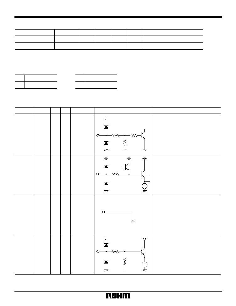
Pin descriptions and equivalent I / O circuits
Pin. No
Pin name
IN
OUT Standard potential
Equivalent I / O circuit
Pin description
1
MUTEA
MUTEB
K
--
--
K
--
2.0V
K
--
2.0V
--
--
0V
1
8
2
7
3
4
5
INA
INB
GND
Mute control pin
When MUTE A (pin 1) goes high, all
three channels are muted at the same
time. When MUTE B (pin 8) goes
high, OUTB and the MIXOUT chroma
signals are muted.
Signal input pin
This is the input pin for the composite
Y signal (sync-tip clamp input).
Ground pin
Signal input pin
Bias-type input pin for the chroma
signal. The input impedance is 20k
.
15k
8k
20k
GND