
Dimension
(Units:mm)
Description
Applications
Features
Variable output, negative voltage IC
BD6111FV
99W028A
Maximum applied power supply voltage
Power dissipation
Operating temperature range
Storage temperature
V
BAT
Pd
Topr
Tstg
V
IN
V
∞C
∞C
Unit
V
mW
300
-20
+70
-55
+125
Symbol
Limits
-0.3
+6.0
-0.3
+6.0
Parameter
Maximum applied input voltage
~
~
~
~
Absolute Maximum Ratings (Ta=25
∞C
)
*
December, 1999
The BD6111FV is a charge-pump, negative supply IC
containing a regulator. The charge pump block inverts
a positive power supply voltage that is inputted to
VBAT pin into a negative voltage and outputs it from
the NEGOUT pin. The regulator block stabilizes this
negative voltage with low-noise and outputs it from
OUT pin. Output voltage values of this regulator can
be controlled by voltage value inputted to VIN pin and
determined by OUT=-1.6 VIN .
1) Highly efficient, built-in inverting charge pump
2) Built-in variable, negative voltage linear regulator.
3) Built-in stand-by switch circuit (pull down resistor 1M
)
4) Compact SSOP-B8 package
SSOP-B8
Compact information computer terminal, such as PDC, PHS and PDA.
Battery driving apparatus requiring negative voltage.
*Derating:3.0mW/∞C for operation above Ta=25∞C.
Power supply voltage
Circuit current
Stand-by current
<Regulator block>
Output voltage
Output ripple voltage
Maximum output current
Load stability
Input stability
VIN pin inflow current
<Charge pump block>
I
Q
1
I
Q
2
Vo
V
RR
Io
MAX
V
OL
V
OI
I
IN
mA
µA
V
dBV
mA
mV
mV
µA
V
BAT
V
2.5
5.5
3
5
-1.9
-60
40
40
2
0.6
-2.0
-70
2
5
0
-2.1
20
No-load, V
IN
=1.25V
No-load, V
IN
=0V, STBY=0V
V
IN
=1.25V, I
OUT
=10mA
V
IN
=1.25V, I
OUT
=10mA
V
IN
=1.25V, V
OUT
Vo+0.1V
V
IN
=1.25V, Io=0~10mA
V
IN
=1.25V
(Unless otherwise noted: Ta=25∞C, V
BAT
=3.6V, STBY=3.6V)
Recommended Operating Conditions (Ta=25
∞C
)
Electrical characteristics
Conditions
Parameter
Symbol
Unit
Min.
Typ.
Max.
Parameter
Symbol
Unit
Min.
Typ.
Max.
Oscillation frequency
Voltage conversion efficiency
Stand-by pin pull down resistor
Stand-by pin
Control voltage
Operation
fosc
V
CE
R
STBY
V
IH
V
IL
kHz
%
M
V
V
1.6
0.3
120
97
1.0
0.6
2.0
-0.3
No-load, NEGOUT monitor
Non-operation
-
-
-
-
-
-
-
-
-
-
-
-
-
-
-
-
-
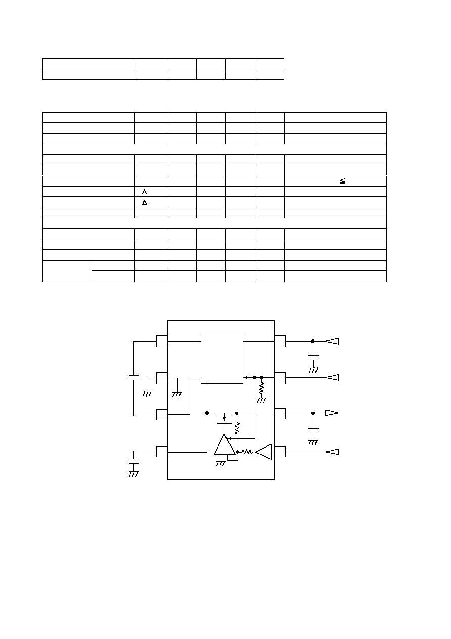
Application circuit
C1
1
µ
C+
GND
C-
NEGOUT
C2
1
µ
1
CHARGE
PUMP
2
3
4
STBY
OUT
8
V
BAT
V
IN
C4
1
µ
7
+
6
+
C3
1
µ
5
1M
1.6M
1M
BD6111FV
-