 | ÐлекÑÑоннÑй компоненÑ: BP5222X | СкаÑаÑÑ:  PDF PDF  ZIP ZIP |
Äîêóìåíòàöèÿ è îïèñàíèÿ www.docs.chipfind.ru
BP5220 / BP5221 / BP5222 /
BP5220X / BP5221X / BP5222X
The BP5220, BP5221, BP5222, BP5220X, BP5221X, and BP5222X are DC / DC converters that use a pulse
width modulation (PWM) system. They contain control circuits, switching devices, rectifiers, and coils, and operate
by only connecting an I / O smoothing capacitor. With a high efficiency of power conversion, the modules are
available in stand-alone 9-pin SIP packages with no heat sink required. They can be applied to various purposes
by fine-adjusting the output voltage and switching on and off. With a wide range of input voltage, the modules are
best suited for obtaining a stable local power supply from a main power supply with a large voltage variation.
Applications
Power supplies for copiers, personal computers, facsimiles, AV equipment, measuring instruments, vending
machines, security device, registers, industrial equipment, and maintenance tools
Features
1) Wide range of input voltage.
5) Small number of external components required.
2) High power conversion efficiency.
6) Heat sink unnecessary.
3) Built-in output ON / OFF switch.
7) Compact package.
4) Applicable to various purposes by
BP5220 / BP5221 / BP5222 : SIP9
fine-adjusting the output voltage.
BP5220X / BP5221X / BP5222X : SIP9
(L-shaped lead type)
List of the series
DC / DC converter
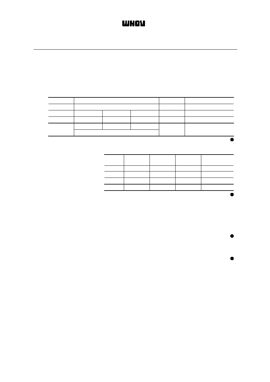
Absolute maximum ratings (Ta=25
°
C)
BP5220 / BP5220X BP5221 / BP5221X BP5222 / BP5222X
Input voltage
8~38
8~38
15~38
V
Output voltage
5
5
12
V
Output current
1
0.5
0.5
A
Power conversion
effciency
85
(V
IN
=15V)
(V
IN
=15V)
(V
IN
=20V)
84
90
%
Unit
Parameter
Symbol
Limits
Unit
BP5220 / BP5220X
BP5221 / BP5221X
BP5222 / BP5222X
Input voltage
V
IN
8~38
8~38
15~38
V
Output current
I
O
1
0.5
0.5
A
°
C
Operating temperature range
Topr
-
20~
+
70
Storage temperature range
Tstg
-
25~
+
80
°
C
1/8
BP5220 / BP5221 / BP5222 /
BP5220X / BP5221X / BP5222X
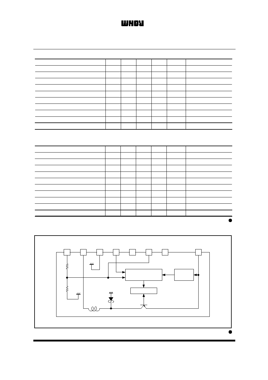
Electrical characteristics BP5220 / BP5220X
(Unless otherwise noted: V
IN
=15V, I
O
=0.5A, SW=1, Ta=25
°
C)
Block diagram
DRIVE CIRCUIT
CONTROL CIRCUIT
POWER
SUPPLY
CIRCUIT
V
IN
9
7
6
5
4
3
2
1
ADJ
CTL
GND
V
OUT
FB
BP5220 / BP5221 / BP5222
N. C.
N. C.
N. C.
Parameter
Symbol
Unit
Conditions
Min.
Typ.
Max.
Input voltage
V
IN
8
-
38
V
Output voltage
V
O
4.75
5
5.25
V
Output current
I
O
-
-
1
A
Line regulation
V
O1
-
35
80
mV
V
IN
=8V~38V
Load regulation
V
O2
-
20
80
mV
I
O
=0.1A~1A
Output ripple voltage
-
30
70
mV
PP
Power conversion efficiency
75
85
-
%
I
O
=1A
Switching frequency
f
SW
-
190
-
kHz
CTL pin ON resistance
R
ON
-
-
4.7
k
V
O
>
4.75V
CTL pin OFF resistance
R
OFF
200
-
-
k
V
O
<
0.1V, SW=2 select
r
V
IN
<
30V
1
2
2 Pulse noise not included.
BP5221 / BP5221X
(Unless otherwise noted: V
IN
=15V, I
O
=0.25A, SW=1, Ta=25
°
C)
Parameter
Symbol
Unit
Conditions
Min.
Typ.
Max.
Input voltage
V
IN
8
-
38
V
Output voltage
V
O
4.75
5
5.25
V
Output current
I
O
-
-
0.5
A
Line regulation
V
O1
-
35
80
mV
V
IN
=8V~38V
Load regulation
V
O2
-
20
80
mV
I
O
=0.05A~0.5A
Output ripple voltage
-
30
70
mV
PP
Power conversion efficiency
70
84
-
%
I
O
=0.5A
Switching frequency
f
SW
-
190
-
kHz
CTL pin ON resistance
R
ON
-
-
4.7
k
V
O
>
4.75V
CTL pin OFF resistance
R
OFF
200
-
-
k
V
O
<
0.1V, SW=2 select
r
1
2
2 Pulse noise not included.
1 Derating required according to the input voltage and ambient temperature.
1 Derating required according to the input voltage and ambient temperature.
2/8
BP5220 / BP5221 / BP5222 /
BP5220X / BP5221X / BP5222X
Measurement circuit
BP5222 / BP5222X
(Unless otherwise noted ; V
IN
=20V, IO=0.25A, SW=1, Ta=25
°
C)
Parameter
Symbol
Unit
Conditions
Min.
Typ.
Max.
Input voltage
V
IN
15
-
38
V
Output voltage
V
O
11.2
12
12.8
V
Output current
I
O
-
-
0.5
A
Line regulation
V
O1
-
22
80
mV
V
IN
=15V~38V
Load regulation
V
O2
-
45
80
mV
I
O
=0.05A~0.5A
Output ripple voltage
-
35
70
Power conversion efficiency
75
90
-
%
I
O
=0.5A
Switching frequency
f
SW
-
190
-
kHz
CTL pin ON resistance
R
ON
-
-
4.7
k
V
O
>
11.2V
CTL pin OFF resistance
R
OFF
200
-
-
k
V
O
<
0.1V, SW=2 select
mV
PP
2 Pulse noise not included.
r
1 Derating required according to the input voltage and ambient temperature.
1
2
2
+
+
9
7
6
5
4
3
2
1
Input
A
V
V
A
f
SW
1
2
0.47
µ
F
Outrput
4.7k
200k
T
Output ripple voltage
BP5220X / BP5221X / BP5222X
BP5220 / BP5221 / BP5222
100
µ
F / 50V
470
µ
F / 50V
Note that output ripple voltage depends on the type and characteristics of the output capacitor.
Switching frequency=1/T
100
µ
F/50V, 470
µ
F/50V ; PL series / NICHIKON(Low-impedance type)
f ; Frequency counter
Fig.1
3/8
BP5220 / BP5221 / BP5222 /
BP5220X / BP5221X / BP5222X
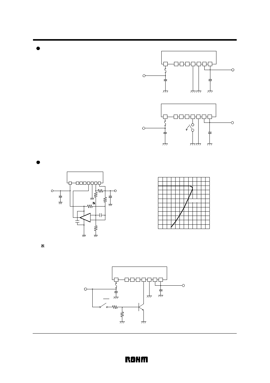
Circuit operation
(1) The basic application examples are shown in Fig.2.
The externally installed parts are only the input and
output smoothing capacitors.
(2) Switching on and off the output voltage is allowed.
The output can be switched off by making pin 4 to
be open (high impedance). (See Fig.3)
(3) Fine adjustment of the output voltage is allowed.
The fine adjustment of output voltage can be
performed from pin 6 via the resistor by connecting
the output terminal (pin 2) or GND.(See application
example3)
Application example
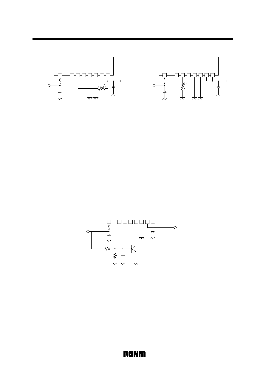
Application example 1 : DC / DC converter with a protection circuit
Application example 2 : Output ON / OFF control
9
7
6
5
4
3
2
1
100
µ
F
470
µ
F
V
IN
V
O
BP5220X / BP5221X / BP5222X
BP5220 / BP5221 / BP5222
+
+
Fig.2
9
7
6
5
4
3
2
1
100
µ
F
470
µ
F
V
IN
SW
V
O
BP5220X / BP5221X / BP5222X
BP5220 / BP5221 / BP5222
OUTPUT
OFF
+
+
Fig.3
470
µ
F
120pF
33k
0.1
µ
F
100
µ
F
1k
0.22
820
COMP.
2.2M
+
-
BA10393
V
IN
24V
V
O
5V
9
7
6
5
4
3
2
1
BP5220X / BP5221X / BP5222X
BP5220 / BP5221 / BP5222
+
+
Fig.4
V
IN
=24V
0.2
0.4
0.6
0.8
1.0
1.2
6
5
4
3
2
1
0
OUTPUT CURRENT (A)
OUTPUT VOLTAGE (V)
Fig.5
9
7
6
5
4
3
2
1
100
µ
F
V
IN
V
O
470
µ
F
100k
100k
2SC1740
BP5220X / BP5221X / BP5222X
BP5220 / BP5221 / BP5222
ON / OFF
+
+
Fig.6
A resistor to secure the rise of output at power on. The resistance to be selected depends on the input voltage.
This is a standard application. Because the control current fluctuates with variations in circuits and components,
set the control current by adding a sufficient margin to the normal current level.
4/8
Be sure to use
fuse for safety
Be sure to use
fuse for safety
Be sure to use
fuse for safety
BP5220 / BP5221 / BP5222 /
BP5220X / BP5221X / BP5222X
Application example 3 : Output voltage fine adjustment
(1) When reducing the output voltage
VR value setting equations(The output voltage after adjustment is denoted Vo.)
(1) When reducing the output voltage
BP5220 / BP5221, BP5220X / BP5221X
R=(V
O
-
1.281) / (0.0278
-
0.00556V
O
) (k
)
BP5222, BP5222X
R=(Vo
-
1.281) / (0.1196
-
0.01Vo) (k
)
(2) When increasing the output voltage
BP5220 / BP5221, BP5220X / BP5221X
R=11160 / (48.4Vo
-
242) (k
)
BP5222, BP5222X
R=1200 / (9.368Vo
-
112) (k
)
To make full use of the ability of the the module products, we recommended the output voltage be
adjusted within
±
20% of the output voltage rating. When the output voltage is increased by 20%, for
instance, the minimum input voltage is also increased by 20%.
(Example : When the output voltage is changed from 5V to 6V in the BP5220, the minimum input voltage
is changed from 8V to 9.6V)
(2) When increasing the output voltage
100
µ
F
V
IN
9
7
6
5
4
3
2
1
470
µ
F
VR
BP5220X / BP5221X / BP5222X
BP5220 / BP5221 / BP5222
V
O
+
+
Fig.7
100
µ
F
V
IN
9
7
6
5
4
3
2
1
470
µ
F
VR
V
O
BP5220X / BP5221X / BP5222X
BP5220 / BP5221 / BP5222
+
+
Fig.8
9
7
6
5
4
3
2
1
100
µ
F
V
O
470
µ
F
100k
C1
10
µ
F
V
IN
24V
470k
BP5220X / BP5221X / BP5222X
BP5220 / BP5221 / BP5222
2SC1740R
+
+
+
Fig.9
Application example 4 : Slow start
The slow start circuit mitigates the pulse load on the internal switching transistor when input voltage is applied,
and rises the output voltage gradually by starting the switching operation slowly.
This application is useful for preventing the malfunction of an external protection circuit due to a rush current,
and can serve as a countermeasure against the operation outside the safe operation range.
C1 is a slow-start capacitor for mitigating the over rush current that flows into the modules when the switch is
turned on.
5/8
Be sure to use
fuse for safety
Be sure to use
fuse for safety
Be sure to use
fuse for safety