DTA144VUA / DTA144VKA / DTA144VSA
Transistors
Digital transistor (built-in resistors)
DTA144VUA / DTA144VKA / DTA144VSA
!
!
!
!Features
1) Built-in bias resistors enable the configuration of an
inverter circuit without connecting external input
resistors.
2) The bias resistors consist of thin-film resistors with
complete isolation to allow positive biasing of the input,
and parasitic effects are almost completely eliminated.
3) Only the on / off conditions need to be set for
operation, making device design easy.
4) Higher mounting densities can be achieved.
!
!
!
!Equivalent circuit
OUT
GND(
+
)
IN
OUT
IN
GND(
+
)
R
1
R
2
!
!
!
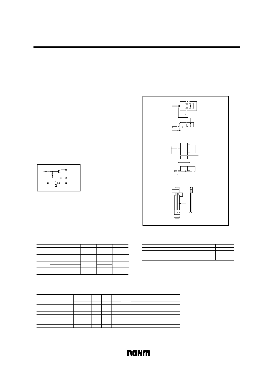
!External dimensions
(Units : mm)
(3) Collector(Drain)
(1) Emitter(Source)
ROHM : UMT3
EIAJ : SC-70
ROHM : SMT3
EIAJ : SC-59
ROHM : SPT
EIAJ : SC-72
DTA144VUA
DTA144VKA
DTA144VSA
(2) Base(Gate)
Each lead has same dimensions
1.25
2.1
0.3
0.15
0to0.1
0.1to0.4
( 3
)
0.9
0.7
0.2
0.65
( 2
)
2.0
1.3
( 1
)
0.65
(2) Base(Gate)
(3) Collector(Drain)
(1) Emitter(Source)
Each lead has same dimensions
0.8
0.15
0to0.1
0.3to0.6
1.1
( 2
)
( 1
)
2.8
1.6
0.4
( 3
)
2.9
1.9
0.95
0.95
0.45
2.5
(1) (2) (3)
(3) Base
(1) Emitter
(2) Collector
( 15Min.
)
5
3
3Min.
Taping specifications
0.45
0.5
4
2
!
!
!
!Absolute maximum ratings
(Ta = 25
�C)
Parameter
Symbol
V
CC
V
I
I
O
I
C(Max.)
Pd
Tj
Tstg
Limits
-
50
-
40~
+
15
-
30
-
10
200
300
DTA144VUA / DTA144VKA
DTA144VSA
150
-
55~
+
150
Unit
V
V
mA
mW
�
C
�
C
Supply voltage
Input voltage
Output current
Power
dissipation
Junction temperature
Storage temperature
!
!
!
!Packaging, marking and packaging specifications
Type
DTA144VUA
UMT3
156
T106
3000
DTA144VKA
SMT3
E56
T146
3000
DTA144VSA
SPT
-
TP
5000
Package
Marking
Packaging code
Basic ordering unit (pieces)
!
!
!
!Electrical characteristics
(Ta = 25
�C)
Parameter
Symbol
Min.
Typ.
Max.
Unit
Conditions
V
I(off)
V
O(on)
I
I
I
O(off)
G
I
f
T
R
1
-
-
-
-
33
-
32.9
-
-
0.1
-
-
-
250
47
-
1
-
0.3
-
0.16
-
0.5
-
-
61.1
V
V
mA
�
A
-
MHz
k
V
CC
=
-
5V , I
O
=
-
100
�
A
V
I(on)
-
6
-
-
V
O
=
-
0.3V , I
O
=
-
2mA
I
O
=
-
10mA , I
I
=
-
0.5mA
V
I
=
-
5V
V
CC
=
-
50V , V
I
=0V
I
O
=
-
5mA , V
O
=
-
5V
V
CE
=
-
10V , I
E
=5mA , f=100MHz
-
R
2
/R
1
0.17
0.21
0.26
-
-
Input voltage
Output voltage
Input current
Output current
DC current gain
Transition frequency
Input resistance
Transition frequency of the device.
Resistance ratio