 | –≠–ª–µ–∫—Ç—Ä–æ–Ω–Ω—ã–π –∫–æ–º–ø–æ–Ω–µ–Ω—Ç: SDU20N03L | –°–∫–∞—á–∞—Ç—å:  PDF PDF  ZIP ZIP |
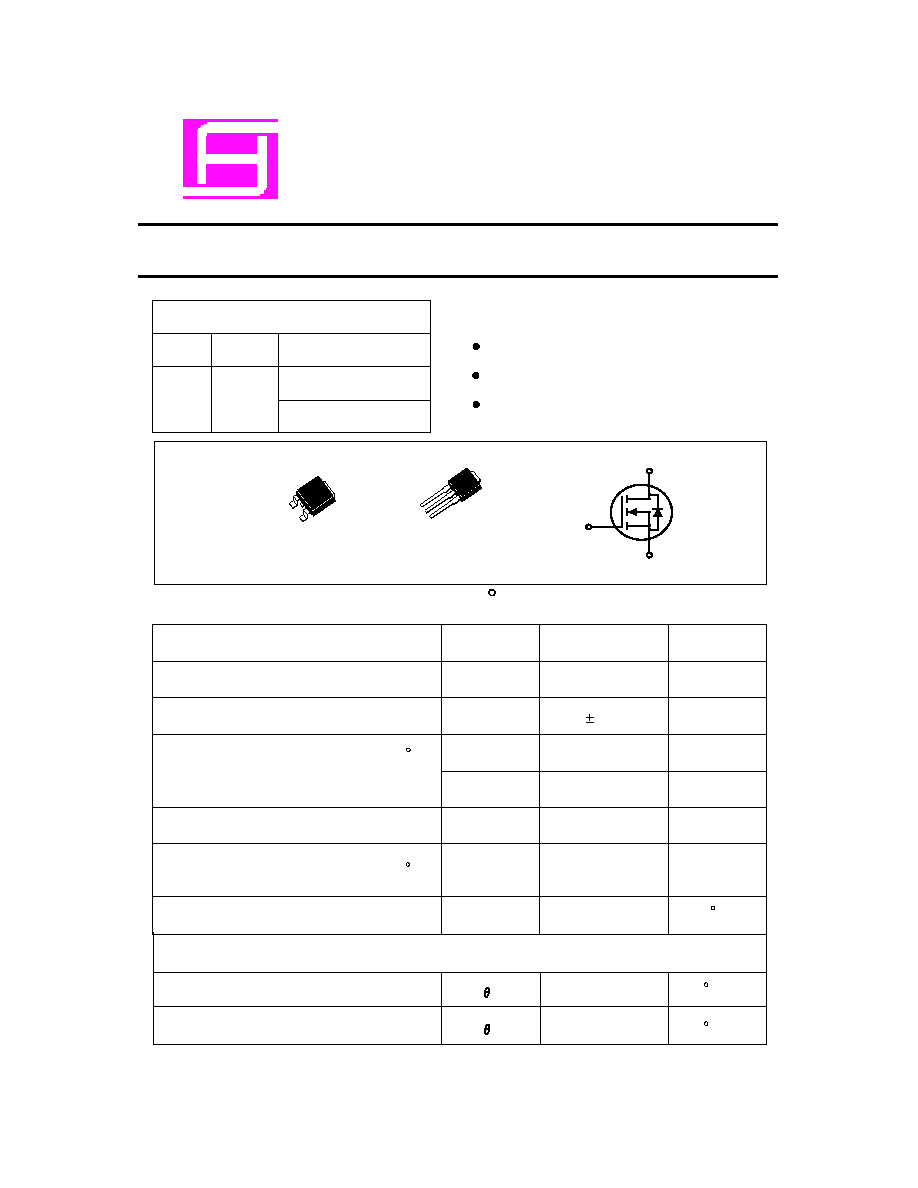
N-Channel Logic Level Enhancement Mode Field Effect Transistor
TO-252 and TO-251 Package.
ABSOLUTE MAXIMUM RATINGS (T
C
=25 C unless otherwise noted)
SamHop Microelectronics Corp.
July 2004 ver1.2
1
PRODUCT SUMMARY
V
DSS
I
D
R
DS(ON) ( m
W
)
30V
35A
15 @ V
GS
= 10V
32 @ V
GS
= 4.5V
FEATURES
Super high dense cell design for low R
DS(ON
).
Rugged and reliable.
S
G
D
SDU SERIES
TO-252AA(D-PAK)
SDD SERIES
TO-251(l-PAK)
G
G
S
S
D
D
SDU/D20N03L
THERMAL CHARACTERISTICS
Thermal Resistance, Junction-to-Case
Thermal Resistance, Junction-to-Ambient
R
JC
3
50
R
JA
/W
C
/W
C
30
Parameter
Symbol
Limit
Unit
Drain-Source Voltage
V
DS
V
Gate-Source Voltage
20
V
GS
V
-Pulsed
35
I
D
A
87
I
DM
A
Drain-Source Diode Forward Current
20
I
S
A
Maximum Power Dissipation
P
D
W
Operating and Storage Temperature Range
T
J
, T
STG
-55 to 175
C
@Tc=25 C
50
Drain Current-Continuous @TJ=125 C
a
Max
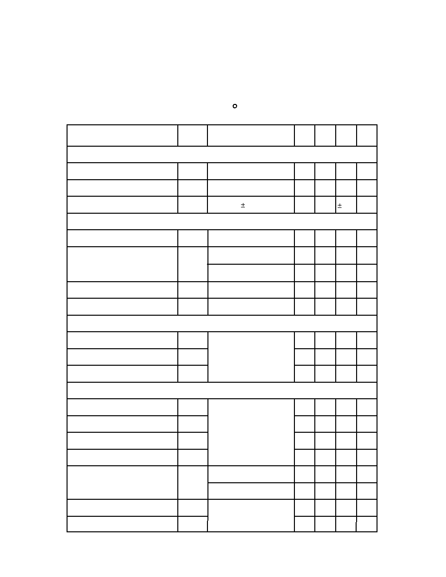
S DU/D20N03L
E LE CTR ICAL CHAR ACTE R IS TICS (T
C
=25 C unless otherwise noted)
Parameter
Symbol
Condition
Min Typ Max Unit
OFF CHAR ACTER ISTICS
Drain-Source Breakdown Voltage
BV
DSS
V
GS
= 0V, I
D
= 250uA
30
V
Zero Gate Voltage Drain Current
I
DSS
V
DS
= 24V, V
GS
= 0V
10
uA
Gate-Body Leakage
I
GSS
V
GS
= 20V, V
DS
= 0V
nA
ON CHAR ACTER ISTICS
a
Gate Threshold Voltage
V
GS(th)
V
DS
= V
GS
, I
D
= 250uA
1
1.5
13.5
23
3
V
Drain-Source On-State R esistance
R
DS(ON)
V
GS
= 10V, I
D
=10A
V
GS
= 4.5V, I
D
= 8A
15
32
On-State Drain Current
I
D(ON)
V
DS
= 10V, V
GS
= 10V
55
25
A
S
Forward Transconductance
FS
g
V
DS
= 10V, I
D
= 20A
DYNAMIC CHAR ACTER ISTICS
b
Input Capacitance
C
ISS
C
R SS
C
OSS
Output Capacitance
R everse Transfer Capacitance
V
DD
=15V, V
GS
= 0V
f = 1.0MH
Z
930
400
120
30
20
34
10
26.5
4.8
5.4
P
F
P
F
P
F
SWITCHING CHAR ACTER ISTICS
b
Turn-On Delay Time
R ise Time
Turn-Off Delay Time
t
D(ON)
t
r
t
D(OFF)
t
f
Fall time
V
DD
= 15V
I
D
=1A
V
GS
= 10V
V
GEN
= 6
ns
ns
ns
ns
Total Gate Charge
Gate-Source Charge
Gate-Drain Charge
Q
g
Q
gs
Q
gd
V
DS
= 15V, I
D
= 20A
V
GS
=10V
nC
nC
nC
2
100
m ohm
m ohm
ohm
nC
V
DS
= 15V,I
D
= 20A,V
GS
=10V
V
DS
= 15V,I
D
= 20A,V
GS
=4.5V
13.5
Parameter
S ymbol
Condition
Min Typ Max Unit
E LE CTR ICAL CHAR ACTE R IS TICS (T
C
=25 C unless otherwise noted)
DR AIN-S OUR CE DIODE CHAR ACTE R IS TICS
Diode Forward Voltage
V
S D
V
GS
= 0V, Is = 20A
1.3
V
a
Notes
b.Guaranteed by design, not subject to production testing.
a.Pulse Test:Pulse Width 300us, Duty Cycle 2%.
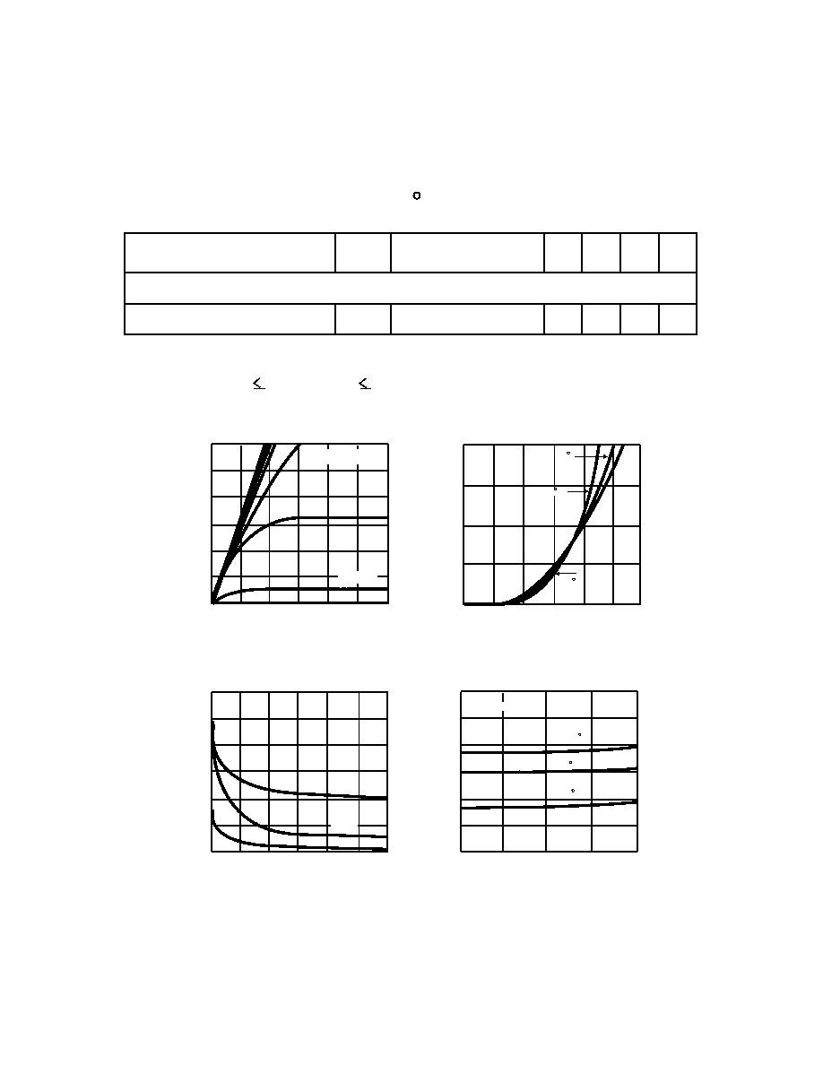
F igure 1. Output C haracteristics
F igure 2. Transfer C haracteristics
F igure 4. On-R esistance Variation with
Drain C urrent and Temperature
F igure 3. C apacitance
V
DS
, Drain-to S ource Voltage (V )
V
G S
, G ate-to-S ource Voltage (V )
V
DS
, Drain-to-S ource Voltage (V )
I
D
, Drain C urrent(A)
C
,
C
a
p
a
c
i
t
a
n
c
e
(
p
F
)
D
r
a
i
n
-
S
o
u
r
c
e
,
O
n
-
R
e
s
i
s
t
a
n
c
e
I
D
,
D
r
a
i
n
C
u
r
r
e
n
t
(
A
)
I
D
,
D
r
a
i
n
C
u
r
r
e
n
t
(
A
)
3
R
D
S
(
O
N
)
,
N
o
r
m
a
l
i
z
e
d
S DU/D20N03L
0 5 10 15 20 25 30
2400
2000
1600
1200
800
400
0
60
50
40
30
20
10
0
0
1
2
3
4
5
6
-55 C
25 C
40
30
20
10
0
0
1
2
3
4
5
6
T j=125 C
1.3
1.2
1.1
1.0
0.9
0.8
0.7
25 C
T j=125 C
-55 C
0
10
20
30
40
V
G S
=10V
V
G S
=10,9,8,7,6,5,4V
V
G S
=3V
C iss
C oss
C rss
S DU/D20N03L
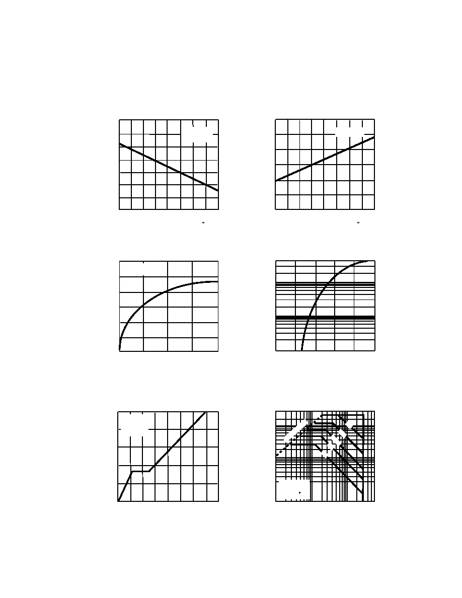
F igure 5. G ate T hres hold V ariation
with T emperature
F igure 6. B reakdown V oltage V ariation
with T emperature
V
t
h
,
N
o
r
m
a
l
i
z
e
d
G
a
t
e
-
S
o
u
r
c
e
T
h
r
e
s
h
o
l
d
V
o
l
t
a
g
e
g
F
S
,
T
r
a
n
s
c
o
n
d
u
c
t
a
n
c
e
(
S
)
V
G
S
,
G
a
t
e
t
o
S
o
u
r
c
e
V
o
l
t
a
g
e
(
V
)
B
V
D
S
S
,
N
o
r
m
a
l
i
z
e
d
D
r
a
i
n
-
S
o
u
r
c
e
B
r
e
a
k
d
o
w
n
V
o
l
t
a
g
e
I
s
,
S
o
u
r
c
e
-
d
r
a
i
n
c
u
r
r
e
n
t
(
A
)
F igure 7. T rans conductance V ariation
with Drain C urrent
I
DS
, Drain-S ource C urrent (A)
F igure 9. G ate C harge
Qg, T otal G ate C harge (nC )
F igure 10. Maximum S afe
O perating Area
V
DS
, Drain-S ource V oltage (V )
F igure 8. B ody Diode F orward V oltage
V ariation with S ource C urrent
V
S D
, B ody Diode F orward V oltage (V )
T j, J unction T emperature ( C )
T j, J unction T emperature ( C )
I
D
,
D
r
a
i
n
C
u
r
r
e
n
t
(
A
)
4
6
40
10
0.1
1.0
0.4
0.6
0.8
1.0
1.2
1.4
1.15
1.10
1.05
1.00
0.95
0.90
0.85
0.80
-50 -25
0
25
50
75 100 125 150
V
DS
=V
G S
I
D
=250uA
-50 -25
0
25
50
75 100 125 150
1.15
1.10
1.05
1.00
0.95
0.90
0.85
I
D
=250uA
40
30
20
10
50
60
0
0
5
10
15
20
V
DS
=10V
10
8
6
4
2
0
0
4
8
12 16 20
24
28 32
V
DS
=15V
I
D
=20A
100
10
1
0.1
0.1
1
10
30
60
V
G S
=10V
S ingle P ulse
Tc=25 C
R
DS
(O
N)
Li
mi
t
DC
1s
100
ms
10m
s
1m
s
50
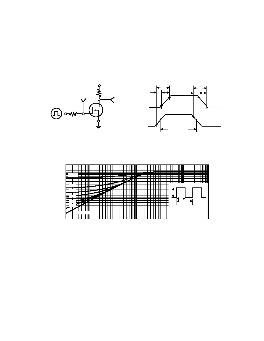
F igure 11. S witching T est C ircuit
F igure 12. S witching Waveforms
t
V
V
t
t
d(on)
OUT
IN
on
r
10%
t
d(off)
90%
10%
10%
50%
50%
90%
t
off
t
f
90%
PULS E WIDTH
T
r
a
n
s
i
e
n
t
T
h
e
r
m
a
l
I
m
p
e
d
a
n
c
e
S quare Wave P ulse Duration (sec)
F igure 13. Normalized T hermal T ransient Impedance C urve
r
(
t
)
,
N
o
r
m
a
l
i
z
e
d
E
f
f
e
c
t
i
v
e
5
6
S DU/D20N03L
INVE R TE D
2
1
0.1
0.01
10
-5
10
-4
10
-3
10
-2
10
-1
1
10
D=0.5
0.2
0.1
0.05
0.02
0.01
P
DM
t
1
t
2
1. R
J A
(t)=r (t) * R
J A
2. R
J A
=S ee Datasheet
3. T
J M-
T
A
= P
DM
* R
J A
(t)
4. Duty C ycle, D=t
1
/t
2
S ING LE P ULS E
V
DD
R
D
V
V
R
S
V
G
G S
IN
G E N
OUT
L
6
S DU/D20N03L
5
35
9
3
95
05
7
41
7
85
30
3
84
0.94
3
3
4
5
9
3
9
1
6.00
0
36
4
9.70
1
82
398
1.425
1.625
56
0.064
0.650
0.850
6
33
L2
0.600
0.024
REF.
REF.
2.29
BSC
0.090
BSC
7
S DU/D20N03L
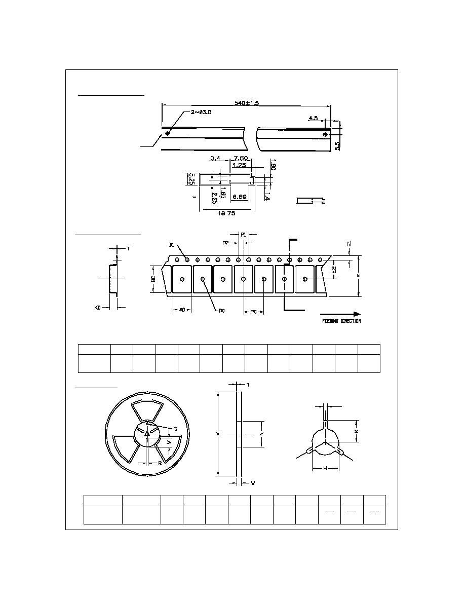
TO251 Tube/TO-252
TO-252 Carrier Tape
TO-252 Reel
Tape and Reel Data
UNIT:
PACKAGE
TO-252
(16 )
A0
B0
K0
D0
D1
E
E1
E2
P0
P1
P2
T
6.80
±
0.1
10.3
±
0.1
2.50
±
0.1
2
1.5
+ 0.1
- 0
16.0
0.3±
1.75
0.1±
7.5
±
0.15
8.0
±
0.1
4.0
±
0.1
2.0
±
0.15
0.3
±
0.05
UNIT:
TAPE SIZE
16
REEL SIZE
330
M
N
W
T
H
K
S
G
R
V
330
± 0.5
97
±
1.0
17.0
+ 1.5
- 0
2.2
13.0
+ 0.5
- 0.2
10.6
2.0
±
0.5
S
8
S DU/D20N03L
" A"
TO-251 Tube