
184pin Unbuffered DDR SDRAM MODULE
M368L6423BT1
Rev. 1.1 May. 2002
512MB DDR SDRAM MODULE
Unbuffered 184pin DIMM
(64Mx64(32Mx64*2 bank) based on 32Mx8 DDR SDRAM)
64-bit Non-ECC/Parity
Revision 1.1
May. 2002
184pin Unbuffered DDR SDRAM MODULE
M368L6423BT1
Rev. 1.1 May. 2002
Revision History
Revision 0 (Aug 1998)
1. First release for internal usage
Revision 0.1 (Aug. 1999)
1. Modified binning policy
From To
-Z (133Mhz) -Z (133Mhz/266Mbps@CL=2)
-8 (125Mhz) -Y (133Mhz/266Mbps@CL=2.5)
-0 (100Mhz) -0 (100Mhz/200Mbps@CL=2)
2.Modified the following AC spec values
*1
: Changed description method for the same functionality. This means no difference from the previous version.
3.Changed the following AC parameter symbol From tDQCK To tAC
Output data access time from CK/CK
Revision 0.2 (Sept. 1999)
1. Changed the odering information.
1-1. Exclude KM mark.
From To
KMM368... M368.....
1-2. PCB Revison
From To
- Blank: 1st generation - 0: 1st gernation
- A : 2nd generation - 1: 2nd generation
- B : 2nd generation - 2: 3nd generation
Example:KMM368L6423AT M368L6423AT0
1-3. Modified binning policy
From To
- 0 (100Mhz/200Mbps@CL=2) - A0 (100Mhz/200Mbps@CL=2)
- Z (133Mhz/266Mbps@CL=2) - A2 (133Mhz/266Mbps@CL=2)
- Y (133Mhz/266Mbps@CL=2.5) - B0 (133Mhz/266Mbps@CL=2.5)
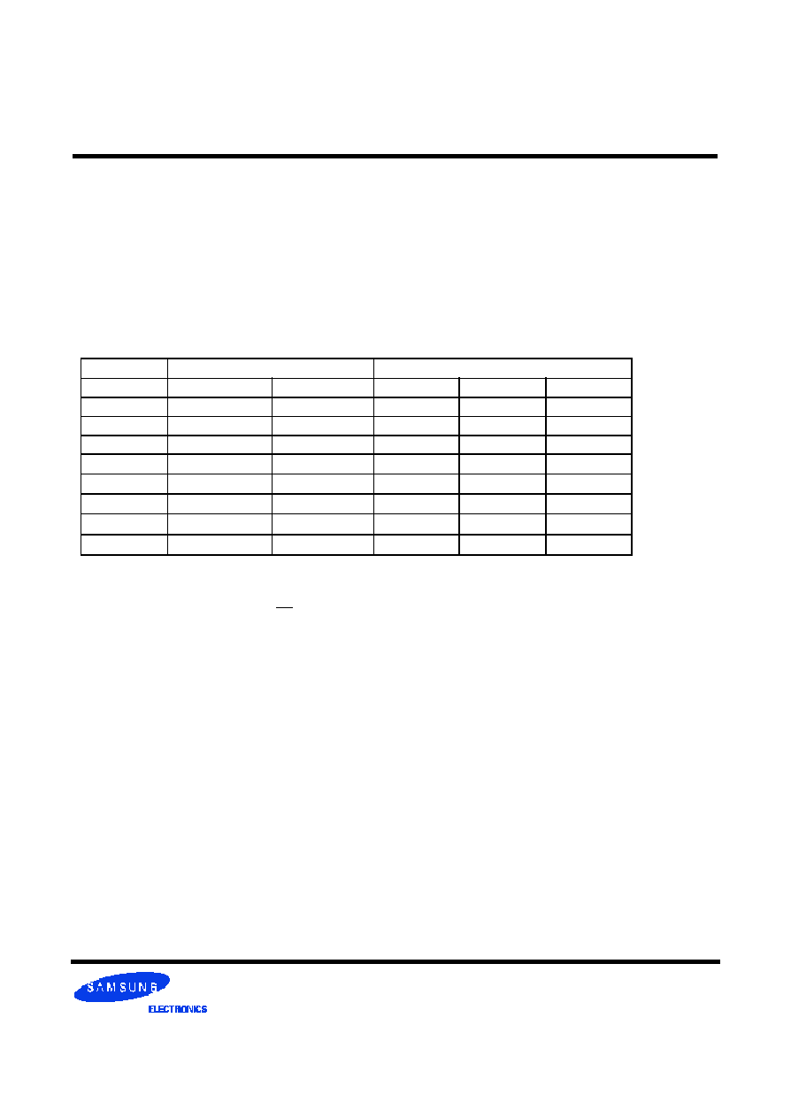
From.
To.
-Z
-0
-Z
-Y
-0
tAC
+/- 0.75ns
+/- 1ns
+/- 0.75ns
+/- 0.75ns
+/- 0.8ns
tDQSCK
+/- 0.75ns
+/- 1ns
+/- 0.75ns
+/- 0.75ns
+/- 0.8ns
tDQSQ
+/- 0.5ns
+/- 0.75ns
+/- 0.5ns
+/- 0.5ns
+/- 0.6ns
tDS/tDH
0.5 ns
0.75 ns
0.5 ns
0.5 ns
0.6 ns
tCDLR
*1
2.5tCK-tDQSS
2.5tCK-tDQSS
1tCK
1tCK
1tCK
tPRE
*1
1tCK +/- 0.75ns
1tCK +/- 1ns
0.9/1.1 tCK
0.9/1.1 tCK
0.9/1.1 tCK
tRPST
*1
tCK/2 +/- 0.75ns
tCK/2 +/- 1ns
0.4/0.6 tCK
0.4/0.6 tCK
0.4/0.6 tCK
tHZQ
*1
tCK/2 +/- 0.75ns
tCK/2 +/- 1ns
+/- 0.75ns
+/- 0.75ns
+/-0.8ns

184pin Unbuffered DDR SDRAM MODULE
M368L6423BT1
Rev. 1.1 May. 2002
Revision 0.3 (December. 1999)
1. Changed from 3.3V to 2.5V in VDDSPD power.
Revision 0.4 (April. 2000)
< Page 3 >
1. Changed from 1450mil to 1250mil in PCB height.
2. Changed pin 90 from WP to NC in pin configuration table.
3. Changed in pin configuration table as followings.
pin 16 : CK0 -> CK1
pin 17 : CK0 -> /CK1
pin 137 : CK1 -> CK0
pin 138 : CK1 -> /CK0
4. Removed WP in pin description.
< Page 4>
5. Changed Clock wiring as followings.
CK0 / CK0 6SDRAMs -> 4SDRAMs
CK1 / CK1 4SDRAMs -> 6SDRAMs
6. Changed bypassing to reflect common Vdd/Vddq plane.
7. Added A13, BA1.
8. Removed WP from serial PD.
< Page 5>
9.
Changed Power & DC operating condition.
< Page 6 >
10. Added Overshoot/Undershoot spec
. Vih(max) = 4.2V, the overshoot voltage duration is
3ns at VDD.
. Vil(min) =- 1.5V, the overshoot voltage duration is
3ns at VSS.
< Page 6,7 >
11.Changed AC operating conditions as follows.
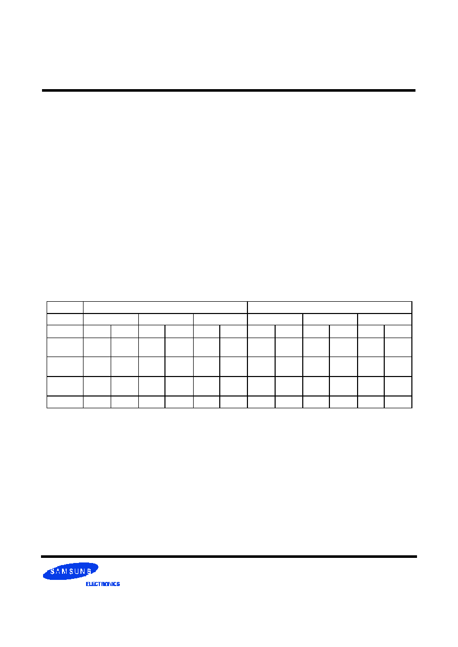
Parameter
Symbol
From
To
Min
Max
Min
Max
I/O Reference voltage
V
REF
1.15
1.35
0.49*VDDQ
0.51*VDDQ
Input logic high voltage
V
IH
(DC)
V
REF
+0.18
V
DDQ
+0.3
V
REF
+0.15
V
DDQ
+0.3
Input logic low voltage
V
IL
(DC)
-0.3
V
REF
-0.18
-0.3
V
REF
-0.15
Input leakage current
I
I
-5
5
-2
2
Output High Current (V
OUT
= 1.95V)
I
O H
-15.2
-16.8
Output Low Current (V
OUT
= 0.35V)
I
OL
15.2
16.8
Parameter/Condition
Symbol
From
To
Min
Max
Min
Max
Input High (Logic 1) Voltage, DQ, DQS and DM signals VIH(AC)
VREF + 0.35
VREF + 0.31
Input Low (Logic 0) Voltage, DQ, DQS and DM signals. VIL(AC)
VREF - 0.35
VREF - 0.31
Input Differential Voltage, CK and CK inputs
VID(AC)
0.7
VDDQ+0.6
0.62
VDDQ+0.6

184pin Unbuffered DDR SDRAM MODULE
M368L6423BT1
Rev. 1.1 May. 2002
< Page 7 >
12. Changed Input/Output capacitance as follows.
< page 8, 9>
13. Changed AC parameters as follows.
14. Added AC parameters as follows
< Page 12>
15.Changed from 1450mil to 1250mil in Package dimension.
Revision 0.5 (April. 2000)
1. Changed from A-die to B-die.
Revision 0.6 (June. 2000)
1. Changed PCB version from T0 to T1.
Parameter
Symbol
From
To
Min
Max
Min
Max
Input capacitance(A
0
~ A
12
, BA
0
~ BA
1
,RAS,CAS, W E )
C
IN1
-
90
65
81
Input capacitance(CKE
0,
CKE
1
)
C
IN2
-
62
42
50
Input capacitance(
CS
0
,CS
1
)
C
IN3
-
55
42
50
Input capacitance(
CLK
0
, CLK
1,
CLK
2
)
C
IN4
-
38
27
34
Data & DQS input/output capacitance(DQ
0
~DQ
63
)
C
OUT
-
16
10
13
Input capacitance(DM
0
~DM
8
)
C
IN5
-
16
10
13
Parameter
from
to
Comments
tDQSQ
+/- 0.5(PC266), +/- 0.6(PC200)
+0.5(PC266), +0.6(PC200)
tDV
+/- 0.35tCK
-
Removed
Parameter
Symbol
-A2(PC266@CL=2)
-B0(PC266@CL=2.5)
-A0(PC200@CL=2)
Min
Max
Min
Max
Min
Max
Output DQS valid window
tQH
tHPmin
-0.75ns
-
tHPmin
-0.75ns
-
tHPmin
-1.0ns
-
Clock half period
tHP
tCLmin
or
tCHmin
-
tCLmin
or
tCHmin
-
tCLmin
or
tCHmin
-
QFC setup to first DQS edge on reads
tQCS
0.9
1.1
0.9
1.1
0.9
1.1
QFC hold after last DQS edge on reads
tDQCH
0.4
0.6
0.4
0.6
0.4
0.6
Write command to QFC delay on write
tQCSW
4.0
4.0
4.0
Write burst end to QFC delay on write
tQCHW
1.25ns
0.5tCK
1.25ns
0.5tCK
1.25ns
0.5tCK
Write burst end to QFC delay on write
interrupted by Precharge
tQCHWI
1.25ns
1.5tCK
1.25ns
1.5tCK
1.25ns
1.5tCK
184pin Unbuffered DDR SDRAM MODULE
M368L6423BT1
Rev. 1.1 May. 2002
Revision 0.7 (October. 2000)
1.Added DC target spec values.
2.Deleted tDAL in AC parameter X.
Revision 0.8 (November. 2000)
1.Changed component placement on module PCB in package dimesions.
Revision 0.9 (June. 2001)
1. Changed module current speificaton
2. Changed typo size on module PCB in package dimesions. (from 2.6mm to 3mm).
3. Changed AC parameter table.
Revision 1.0 (Dec. 2001)
- Add derating values for the specifications if the single-ended clock skew rate is less than 1.0V/ns in page 47.
- Revised "Absolute maximum rating" table in page 38.
. Changed "Voltage on VDDQ supply relative to VSS" value from -0.5~3.6V to -1~3.6V
. Changed "power dissipation" value from 1.0W to 1.5W.
- Revised AC parameter table
- Deleted typical current in IDD spec. table
- Included address and control input setup/hold time(tIS/tIH) at slow slew rate in DDR200/266 AC specification
- Deleted Exit self refresh to write command(tXSW) in DDR200/266 AC specification
- Rename tXSA(exit self refresh to bank active command) to tXSNR(exit self refresh to non read command) at DDR200/266
- Rename tXSR(exit self refresh to read command) to tXSRD at DDR200/266
- Rename tWPREH(DQS in hold time) to tWPRE at DDR200/266
- Rename tREF(Refresh interval time) to tREFI at DDR200/266
- Changed tWR value from 2tCK to 15ns.
--Rename tCDLR(Write data out to Read command) t0 tWTR
- Added tDAL(tWR+tRP)
Revision 1.1 (May. 2002)
1. Change pin location of A13 from pin 103 to pin 167
From
To
DDR266A
DDR266B
DDR200
DDR266A
DDR266B
DDR200
Min.
Max.
Min.
Max.
Min.
Max.
Min.
Max.
Min.
Max.
Min.
Max.
tHZ
tACmin
-400ps
tACmax
-400ps
tACmin
-400ps
tACmax
-400ps
tACmin
-400ps
tACmax
-400ps
-0.75
+0.75
-0.75
+0.75
-0.8
+0.8
tLZ
tACmin
-400ps
tACmax
-400ps
tACmin
-400ps
tACmax
-400ps
tACmin
-400ps
tACmax
-400ps
-0.75
+0.75
-0.75
+0.75
-0.8
+0.8
tWPST
(tCK)
0.25
0.25
0.25
0.4
0.6
0.4
0.6
0.4
0.6
tPDEX
10ns
10ns
10ns
7.5ns
7.5ns
10ns