DUAL LOW NOISE EQ AMP
S1A0211X01
1
INTRODUCTION
The S1A0211X01 is a monolithic integrated circuit consisting of
a 2-channel pre-amplifier in an 8-pin plastic single in-line pack-
age.
FEATURES
∑
Recommended operating supply voltage range:
V
CC
= 5V to 14V
∑
Low noise (V
NI
= 1.0
µ
V: Typ)
∑
High channel separation
∑
Minimum number of external parts required
ORDERING INFORMATION
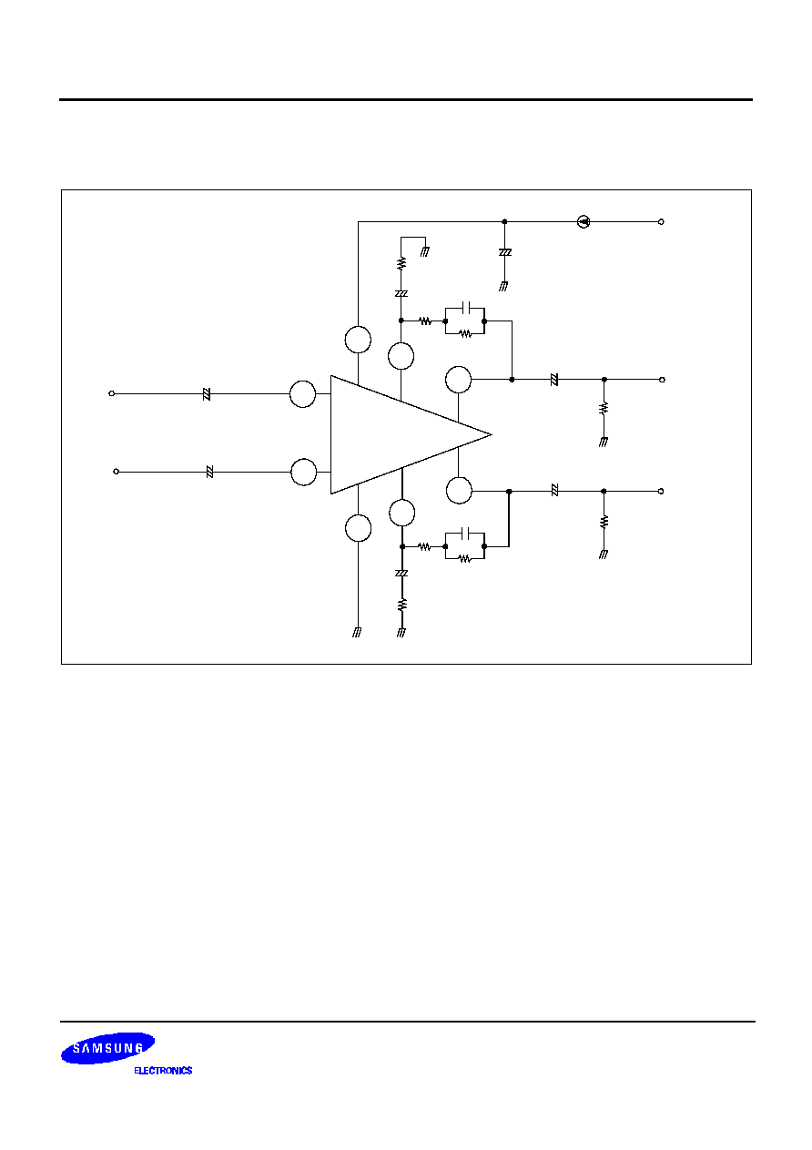
BLOCK DIAGRAM
Device
package
Operating Temperature
S1A0211X01-I0U0
8
-
SlP
-
20
∞
C -- +70
∞
C
8
-
SlP
+
+
1
2
3
4
5
6
7
8
AMP1
AMP2
INPUT1
NF1 OUTPUT1
V
CC
OUTPUT2 NF2
INPUT2
GND

S1A0211X01
DUAL LOW NOISE EQ AMP
2
ABSOLUTE MAXIMUM RATINGS (Ta = 25
∞
C)
ELECTRICAL CHARACTERISTICS
(Ta=25
∞
C, V
CC
= 9V, R
L
= 10k
, R
G
= 600
, f = 1kHz, NAB, unless otherwise specified)
Characteristic
Symbol
Value
Unit
Supply Voltage
V
CC
18
V
Power Dissipation
P
D
200
mW
Operating Temperature
T
OPR
-
20 ≠ + 70
∞
C
Storage Temperature
T
STG
-
40 ≠ + 125
∞
C
Characteristic
Symbol
Test Conditions
Min.
Typ.
Max.
Unit
Quiescent Circuit Current
I
CCQ
V
I
= 0
-
4.0
6.0
mA
Open Loop Voltage Gain
G
VO
-
65
80
-
dB
Closed Loop Voltage Gain
G
VC
V
O
= 0.5V
30
35
37
dB
Output Voltage
V
O
THD = 1%
1.1
1.3
-
V
Total Harmonic Distortion
THD
V
O
= 0.5V
-
0.1
0.3
%
Input Resistance
R
I
-
70
100
-
k
Equivalent Input Noise Voltage
V
NI
R
G
= 2.2k
BW (
-
3dB) = 15Hz
-
30kHz
-
1.0
2.0
µ
V
Cross Talk
CT
R
G
= 2.2k
50
65
-
dB

S1A0211X01
DUAL LOW NOISE EQ AMP
4
APPLICATION INFORMATION
External Components
C
2
(C
9
): Input coupling capacitor
These components are concerned with the output noise and operation starting time. Its capacitance is ade-
quate for 10
µ
F.
As C2 (C9) below 4.7
µ
F extends the operation starting time, a capacitance of over 4.8
µ
F is recommended.
C
3
(C
8
): Negative feedback capacitor
These components decide the low cut-off frequency, which is determined as follows:
A large C
3
(C
8
) makes the operation starting time of an amplifier late. Its capacitance is adequate for 47 F.
C
4
, R
3
, R
2
(C
7
, R
4
, R
5
): Equalizer network
These components decide the frequency response of an equalizer amplifier. The time constant of standard
NAB characteristic is as follows:
C
11
Filter capacitor of the power line
This should be located as close to the supply voltage pin (Pin 4) as possible. The recommended value is 47
µ
F.
C
1
(C
10
): Protection capacitor
These components protect against wave damage of strong electric fields. They also protect against engine
noise damage and block oscillation during high amplifying operations.
C
5
(C
6
): Output coupling capacitor
The recommended value is 10
µ
F.
Tape Speed
Time Constant
9.5 cm/sec
4.75 cm/sec
C
4
(R
2
+ R
3
)
3,180
µ
sec
1,590
µ
sec
C
4
, R
2
90
µ
sec
120
µ
sec
C
3
(C
8
) =
where, f
L
: low cut-off frequency.
1
2
f
L
∑
R
2
(R
7
)