 | –≠–ª–µ–∫—Ç—Ä–æ–Ω–Ω—ã–π –∫–æ–º–ø–æ–Ω–µ–Ω—Ç: S1L9223B | –°–∫–∞—á–∞—Ç—å:  PDF PDF  ZIP ZIP |

RF AMP & SERVO SIGNAL PROCESSOR
S1L9223B01
1
INTORDUCTION
The S1L9223B01 is a 1-chip BICMOS integrated circuit to perform the
function of RF amp and servo signal processor for compact disc
player applications.
It consist of blocks for RF signal processing, focus, tracking,
sled and spindle servo. Also this IC has adjustment free function
and embedded OP-AMP for audio post filter.
FEATURES
∑
RF amplifier & RF equalizer
∑
Focus error amplifier & servo control
∑
Tracking error amplifier & servo control
∑
Mirror & defect detector circuit
∑
Focus OK detector circuit
∑
APC (Auto Laser Power Control) circuit for constant laser power
∑
FE bias & focus servo offset adjustment free
∑
EF balance & tracking error gain adjustment free
∑
Embedded audio post filter
∑
The circuit for Interruption countermeasure
∑
Double speed play available
∑
Operating voltage range: S1L9223B01: 5V
ORDERING INFORMATION
RELATED PRODUCT
∑
S5L9286F01 Data Processor
∑
S5L9284D Data Processor
∑
KA9258D/KA9259D Motor Driver
Device
Package
Temperature Range
S1L9223B01-Q0R0
80-QFP-1420C
-
20 to +70
∞
C
80
-
QFP
-
1420C
S1L9223B01
RF AMP & SERVO SIGNAL PROCESSOR
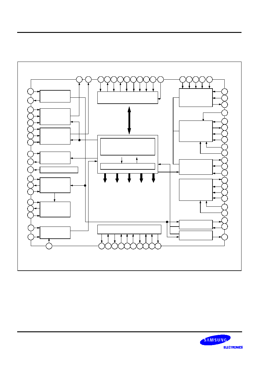
2
BLOCK DIAGRAM
73
74
65
66
63
67
68
79
69
70
71
78
76
75
32
33
77
2
4
RF Amp
59
Focus Error Amp
FE-BIAS Adjustment
Tracking Error Amp
E/F Balance & Gain
Control
APC Amp
LDON
Center Voltage Amp.
RF Level AGC
Equalizer
EFM
Comparator
Defect Detection
Circuit
54
22
30
29
31
38
37
36
35
51
52
58
26
28
27
MICOM Data
Interface Logic
60
47
48
57
49
50
53
55
62
61
43
44
42
46
45
23
24
25
6
39
1
40
5
15
16
13
14
19
17
12
11
9
10
Focus Phase
Compensation
& Offset cancel circuit
Tracking Phase
Compensation Block
& Jump Pulse GEN.
Sled Servo Amplifier
& Sled Kick GEN.
Spindle Servo LPF
( Double Speed )
Mirror Detection
Circuit
FOK Detection
Circuit
MICOM TO SERVO CONTROL
AUTO SEQUENCER
ADJUSTMENT-FREE CONTROL
Built-in Post Filter Amp ( L&R )
FS1~
FS4
TM1~
TM6
BAL1~
BAL5
PS1~
PS4
GA1~
GA5
RF-
RFO
PD1
PD2
F
E
EI
PD
LD
VR
EQO
IRF
ASY
EFM
RFI
DCB
DCC1
GC
1
O
GC
1
I
CH1
O
CH1I
MU
T
E
I
RRC
CH2
O
CH2I
GC
2
I
GC
2
O
FDFCT
FE-
FEO
TDFCT
TE-
TEO
TE2
LPFT
SLO
SL-
SL+
SPDLO
SPDL-
SMDP
SMON
SMEF
FSET
MIRROR
MCP
FOK
TG2
TGU
FE
1
TE
1
ML
T
TZ
C
FE
2
FL
B
FG
D
FS
3
3
&
WD
C
H
TRCNT
LO
CK
IS
T
A
T
R
ESET
MD
A
T
A
MC
K
AT
S
C
FRS
H
DCC2
FEBIAS
EQC

RF AMP & SERVO SIGNAL PROCESSOR
S1L9223B01
3
PIN CONFIGURATION
1
2
3
4
5
6
7
8
9
10 11 12 13 14 15 16 17 18 19 20 21 22 23 24
25
26
27
28
29
30
31
32
33
34
35
36
37
38
39
40
64 63 62 61 60 59 58 57 56 55 54 53 52 51 50 49 48 47 46 45 44 43 42 41
80
79
78
77
76
75
74
73
72
71
70
69
68
67
66
65
S1L9223B01
MC
P
DCB
FR
S
H
DCC2
DCC1
F
SET
VDDA
VCCP
GC2I
GC2O
CH2
I
CH2
O
CH1
O
CH1
I
GC1O
GC1I
RRC
VS
SP
MU
T
E
I
I
SET
VRE
G
WDCK
SM
DP
SM
O
N
SMEF
FLB
FS3
FGD
LOCK
TRCNT
ISTAT
ASY
EFM
VSSA
MCK
MDATA
MLT
RESET
MIRROR
FOK
DVEE
FEBI
AS
TG
2
TG
U
FD
F
C
T
FE
1
FE
2
TD
F
C
T
DVDD
LP
F
T
TE
1
TE
2
TZ
C
AT
S
C
TE
O
TE
-
FE
O
FE
-
SPDL
O
SPDL
-
SL
-
SL
O
SL
+
SST
O
P
GND
EI
EQC
RFI
EQO
IRF
RFO
RF-
VCC
VR
LD
PD
E
F
PD2
PD1

S1L9223B01
RF AMP & SERVO SIGNAL PROCESSOR
4
PIN DESCRIPTION
Pin No.
Symbol
Description
1
MCP
Capacitor connection pin for mirror hold
2
DCB
Capacitor connection pin for defect Bottom hold
3
FRSH
Capacitor connection pin for time constant to generate focus search waveform
4
DCC2
The input pin through capacitor of defect bottom hold output
5
DCC1
The output pin of defect bottom hold
6
FSET
The peak frequency setting pin for focus, tracking servo and cut off frequency of CLV
LPF
7
VDDA
Analog VCC for servo part
8
VCCP
VCC for post filter
9
GC2I
Amplifier negative input pin for gain and low pass filtering of DAC output CH2
10
GC2O
Amplifier output pin for gain and low pass filtering of DAC output CH2
11
CH2I
The input pin for post filter channel2
12
CH2O
The output pin for post filter channel2
13
CH1O
The output pin for post filter channel1
14
CH1I
The input pin for post filter channel1
15
GC1O
Amplifier output pin for gain and low pass filtering of DAC output CH1
16
GC1I
Amplifier negative input pin for gain and low pass filtering of DAC output CH1
17
RRC
The pin for noise reduction of post filter bias
18
VSSP
VSS for post filter
19
MUTEI
The input pin for post filter muting control
20
ISET
The input pin for current setting of focus search, track jump and sled kick voltage
21
VREG
The output pin of regulator
22
WDCK
The clock input pin for auto sequence
23
SMDP
The input pin of CLV control output pin SMDP of DSP
24
SMON
The input pin for spindle servo ON through SMON of DSP
25
SMEF
The input pin of provide for an external LPF time constant
26
FLB
Capacitor connection pin to perform rising low bandwidth of focus loop
27
FS3
The pin for high frequency gain change of focus loop with internal FS3 switch
28
FGD
Reducing high frequency gain with capacitor between FS3 pin
29
LOCK
Sled runaway prevention pin
30
TRCNT
Track count output pin
31
ISTAT
Internal status output pin

RF AMP & SERVO SIGNAL PROCESSOR
S1L9223B01
5
PIN DESCRIPTION
(Continued)
Pin No.
Symbol
Description
32
ASY
The input pin for asymmetry control
33
EFM
EFM comparator output pin
34
VSSA
Analog VSS for servo part
35
MCK
MICOM clock input pin
36
MDATA
MICOM data input pin
37
MLT
MICOM data latch input pin
38
RESET
Reset input pin
39
MIRROR
The mirror output for test
40
FOK
The output pin of focus OK comparator
41
SSTOP
The pin for detection whether pick_up position is innermost or not
42
SL+
The noninverting input pin of sled servo amplifier
43
SLO
The output pin of sled servo amplifier
44
SL-
The inverting input pin of sled servo amplifier
45
SPDL-
The noninverting input pin of spindle servo amplifier
46
SPDLO
The output pin of spindle servo amplifier
47
FE-
The inverting input pin of focus servo amplifier
48
FEO
The output pin of focus servo amplifier
49
TE-
The inverting input pin of tracking servo amplifier
50
TEO
The output pin of tracking servo amplifier
51
ATSC
The input pin for Anti-shock detection
52
TZC
The comaparator input pin for tracking zero crossing detection
53
TE2
Tracking servo input pin
54
TE1
Tracking error amplifier output pin
55
LPFT
The input pin of tracking error low pass filtering signal
56
DVDD
The power supply pin for logic circuit
57
TDFCT
The capacitor connection pin for tracking defect compensation
58
FE2
Focus servo input pin
59
FE1
Focus error amplifier output pin
60
FDFCT
The capacitor connection pin for focus defect compensation
61
TGU
The capacitor connection pin for high frequency tracking gain switch
62
TG2
The pin for high frequency gain change of tracking servo loop with internal TG2 switch