 | ÐлекÑÑоннÑй компоненÑ: S5D2650 | СкаÑаÑÑ:  PDF PDF  ZIP ZIP |
Äîêóìåíòàöèÿ è îïèñàíèÿ www.docs.chipfind.ru
ELECTRONICS
MULTIMEDIA VIDEO
S5D2650 Data Sheet
PAGE 1 OF 95
7/18/03
MULTISTANDARD VIDEO DECODER/SCALER
The S5D2650 converts analog NTSC, PAL or SECAM
video in composite, S-video, or component format to
digitized component video. Output data can be selected for
CCIR 601 or square pixel sample rates in either YCbCr or
RGB formats. The digital video can be scaled down in both
the horizontal and vertical directions. The S5D2650 also
decodes Intercast, Teletext, Closed Caption, and SMPTE
data with a built-in bit data slicer. Digitized CVBS data can
be output directly during VBI for external processing.
FEATURES
· Accepts NTSC-M/N/4.43, PAL-M/N/B/G/H/I/D/K/L and
SECAM formats with auto detection
· 6 analog inputs: 2 S-video, 4 composite, or 2 3-wire
YPbPr component video
· YPbPr Progressive input support(720x480p)
· 3-line luma and chroma comb filters including
adaptive luma comb for NTSC
· Programmable luma bandwidth, contrast,
brightness, and edge enhancement
· Programmable chroma bandwidth, hue, and
saturation
· High quality horizontal and vertical down scaler
· Intercast, Teletext and Closed Caption decoding with
built-in bit slicer
· Direct output of digitized CVBS during VBI for
Intercast application
· Analog square pixel or CCIR 601 sample rates
· Output in 4:4:4, 4:2:2, or 4:1:1 YCbCr component, or
24-bit or 16-bit RGB formats with dithering
· YCbCr 4:2:2 output can be 8 or 16 bits wide with
embedded timing reference code support for 8-bit
mode
· Simultaneous scaled and non-scaled digital output
ports outputs for 8-bit mode.
· Direct access to scaler via bi-directional digital port.
· Programmable Gamma correction table
· Programmable timing signals
· Industry standard IIC interface
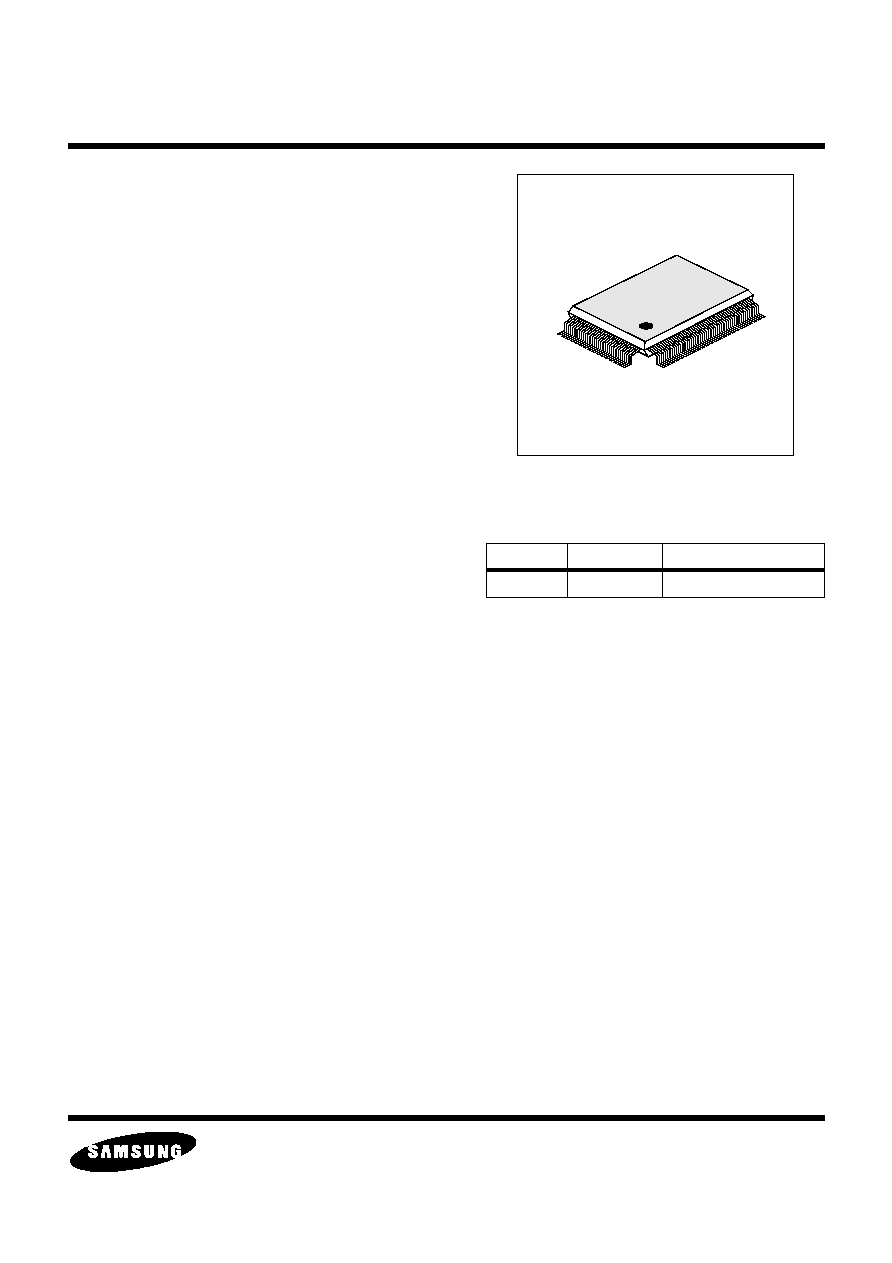
100 PQFP
ORDERING INFORMATION
Device
Package
Temperature Range
S5D2650
100 PQFP
0°~+70°C
APPLICATIONS
· Multimedia
· Digital Video
· Video Capture/Editing
· LCD-TV
· Surveillance system
RELATED PRODUCTS
· KS0123 MULTISTANDARD VIDEO ENCODER
· KS0125 MULTISTANDARD VIDEO ENCODER
· KS0127B VIDEO DECODER
ELECTRONICS
S5D2650 Data Sheet
MULTIMEDIA VIDEO
PAGE 2 OF 95
7/18/03
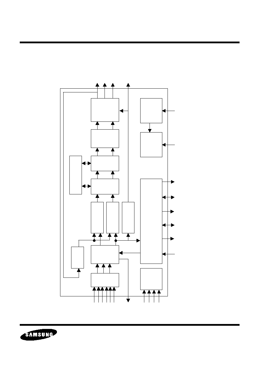
BLOCK DIAGRAM
c{S
c{R
cedS
cedR
cetR cetS
gzx}Y
zOvcn
JTVPWYXojK
ufcv
cgzS
uenm
cgzR
{}Y\R
e}Y\R
eeg
p
eef
c
emT
juS juT jcx gjcx xu xcx gcxc rkf qff
rqtvc rqtvd
em
hknv
q
orT
qgp tuvd
k owz
e cie UOcfeI
kTe j
k
e
r
Jf
jN
ucvK
nwoc
r
Jp
dtvN
eK
xdk
f JeeQvvzK
Tf
e h
u JjQx f uK
{Qe
n
d
e u eP
H
i
q
h JeektXWXN V\V\VQV\T\T
V\S\S tidK
eektXWX
k
f
nOn
e
iPJfvqQrnnK
cieQe
v
iP
f
kQq
gN f e
vguv owz
uecpgp vguv}T\R
ELECTRONICS
S5D2650 Data Sheet
MULTIMEDIA VIDEO
PAGE 3 OF 95
7/18/03
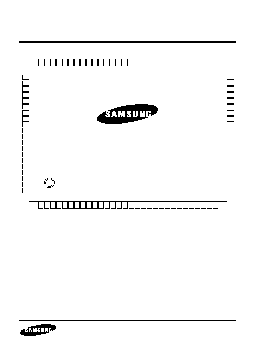
PIN ASSIGNMENT - 100 PQFP
% $# #
% $# #
% $# #
% $# #
& '"$ &'& '
& '"$ &'& '
& '"$ &'& '
& '"$ &'& '
#
# # # # #
# # #
# #
# # # #
#
#
#
#
#
#
##
##
##
##
##
#
#
#
#
#
##
##
##
##
#
#
#
#
#
#
#
#
#
###
# # # #
## ## ## ## ## # # # # #
## ## ## ## ## # # # # # ##
%%$
%%$
%%$
$ #
$$$
$ #
%%$
$$%#
$$$
$$%#
%%$
$$$#
$$$
$$$#
%%%
%%%
$% %#
$$%
%
%%%
%%#
%%#
#
#
#
#
$
$$#
$$#
%%#
%%#
$
$
$#
$#
$#
$#
$#
$
%$$
&
%%#
%%#
#
%%%#
%%%%$
$$#
%%#
#
#
%%#
%%#
$$#
$$#
$#
$#
%$$%
$$$$%
$$
%$
%#
%%#
%%#
%%#
%%#
%%%#
%%%#
#
#
%#
$
%%%%$
%
%$$
$#
$$#
%%#
$
%$
#
%
%%#
%%#
$$#
$$#
%%%
$$#
%$%
%$
%%#
$
$
$
%%#
%%#
ELECTRONICS
S5D2650 Data Sheet
MULTIMEDIA VIDEO
PAGE 4 OF 95
7/18/03
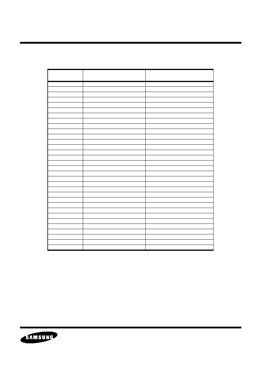
PIN DESCRIPTI O N
Pin Name
Pin #
Type
Description
ANALOG PINS, Reference CLOCK and RESET
AY0
84
I
1 of 4 CVBS or 1of 2 S-video Y inputs or 1of 2 component Y inputs.
AY1
86
I
1 of 4 CVBS or 1of 2 S-video Y inputs or 1of 2 component Y inputs.
ACR0
88
I
1 of 4 CVBS input or 1 of 2 component Pr input
ACR1
90
I
1 of 4 CVBS input or 1 of 2 component Pr input
ACB0
92
I
1 of 2 S-video C inputs or 1 of 2 component Pb input
ACB1
94
I
1 of 2 S-video C inputs or 1 of 2 component Pb input
COMP2
97
O
Internal 1.3 V reference (requires an external 0.1
µ
F capacitor
connected to VSS).
FILT
99
O
Loop filter output for PLL
XTALI
7
I
Crystal or TTL clock input.(24.576MHz or 26.8MHz)
XTALO
8
O
Crystal output.
RSTB
10
I
Chip reset. Active low signal.(5V tolerant Input Pin)
INPUT, OUTPUT and Bi-Directional Pins (All output pins can be selectively tri-stated)
Y0 - Y7, C0 - C7 45-48,53-56,33-
39,44
O
Y[7:0] : Y outputs for CCIR601 or Green out for 24 Bit RGB mode.
C[7:0] : Cb/Cr outputs for CCIR601 or Blue out for 24 Bit RGB mode.
EXV0 - EXV7
16,27,28,61-63,
68,71
I/O
Expanded digital video I/O port. Red data out for 24 Bit RGB mode
or 8 Bit input of CCIR 656 input mode.
HS1
26
I/O
Programmable horizontal sync signal. When the EXV port is
configured as an input, this pin can be programmed as an input.
(default : Output)
HS2
76
O
Programmable horizontal sync signal. (Same as HS1)
VS
23
I/O
Programmable vertical sync signal. When the EXV port is configured
as an input, this pin can be programmed as an input.
(default : Output)
HAV
25
O
Programmable horizontal active video signal.
VAV
3
O
Programmable vertical active video signal.
EHAV
5
O
Valid pixel data flag for horizontal scale down. Active when output
video data is valid.
EVAV
4
O
Valid line data flag for vertical scale down. Active when output video
line is valid.
ODD
22
O
Odd field flag. Polarity is programmable.
ELECTRONICS
S5D2650 Data Sheet
MULTIMEDIA VIDEO
PAGE 5 OF 95
7/18/03
PID
17
O
PAL ID flag. Pahse Alternate Line flag
OEN
15
I
Output data, timing and clock 3-state output control.
(Default : tied to VDD)
CK
18
I/O
System clock. (Default : 27MHz output. When the EXV port is used
as an input, this can be programmed as an input system clock.)
CK2
21
O
Pixel rate output clock (Default : 13.5 MHz)
CCDAT
73
O
Sliced VBI data output. Data can be from Closed Caption, Teletext,
Intercast, or WSS type encoded data.
CCEN
74
O
When high, this pin indicates that valid VBI data is being clocked out
at the CCDAT pin or at the digital video output.
MULTI-PURPOSE I/O PORTS
PORTA
58
I/O
Multi-purpose I/O portA.
PORTB(SCH)
24
I/O
Multi-purpose I/O portB.
HOST INTERFACE
SCLK
75
I
Serial clock for IIC host interface. (5V tolerant schmitt trigger pin)
SDAT
72
I/O
Serial data for IIC host interface.(5V tolerant schmitt triggered open
drain Pins)
AEX0 - AEX1
69 - 70
I
Device ID selection for IIC host interface.
POWER AND GROUND
VDD3
9,20,59
3.3V
Digital power supply for input, output buffers.
VDD1
11,12,42,43,66,
67
1.8V
Digital power supply for core logic.
VDDA
85,89,93
3.3V
Analog power supply for ADC, AGC and reference circuits.
VDDP
98
3.3V
Analog power supply for clock generation circuit(PLL).
VSS
1,2,6,13,14,19,
40,41,49-52,60,
64,65,77-80,
81-83,87,91,95,
96
GND Common ground.
VSSP
100
GND Common ground for PLL.
PIN DESCRIPTION (Continued)
Pin Name
Pin #
Type
Description
ELECTRONICS
S5D2650 Data Sheet
MULTIMEDIA VIDEO
PAGE 6 OF 95
7/18/03
TEST
TEST0
29
I
Test pin 0. For normal use, this pin should be connected to VSS.
TEST1
30
I
Test pin 1. For normal use, this pin should be connected to VSS.
TEST2
57
I
Test pin 2. For normal use, this pin should be connected to VSS.
SCANEN
31
I
SCAN Mode Test pin.For normal use, this pin should be connected
to VSS.
CKE
32
I
For Test TBC function. For normal use, this pin should be connected
to VSS.
PIN DESCRIPTION (Continued)
Pin Name
Pin #
Type
Description
ELECTRONICS
S5D2650 Data Sheet
MULTIMEDIA VIDEO
PAGE 7 OF 95
7/18/03
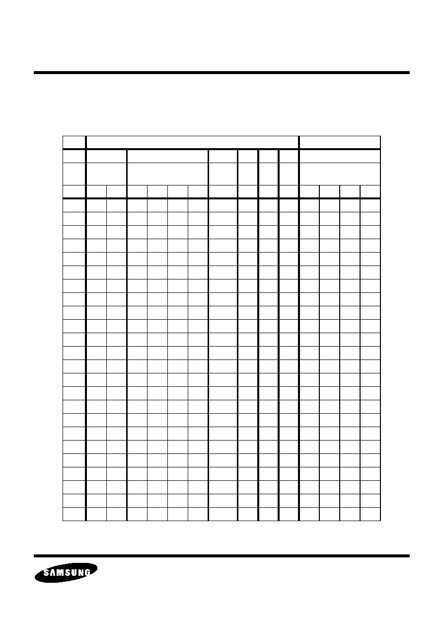
PIN CROSS REFERENCE: NUMERICAL ORDER BY PIN NUMBER
Pin #
Pin Name
Pin #
Pin Name
Pin #
Pin Name
Pin #
Pin Name
1
VSS
26
HS1
51
VSS
76
HS2
2
VSS
27
EXV1
52
VSS
77
VSS
3
VAV
28
EXV2
53
Y4
78
VSS
4
EVAV
29
TEST0
54
Y5
79
VSS
5
EHAV
30
TEST1
55
Y6
80
VSS
6
VSS
31
SCANEN
56
Y7
81
VSS
7
XTALI
32
CKE
57
TEST2
82
VSS
8
XTALO
33
C0
58
PORTA
83
VSS
9
VDD3
34
C1
59
VDD3
84
AY0
10
RST
35
C2
60
VSS
85
VDDA
11
VDD1
36
C3
61
EXV3
86
AY1
12
VDD1
37
C4
62
EXV4
87
VSS
13
VSS
38
C5
63
EXV5
88
ACR0
14
VSS
39
C6
64
VSS
89
VDDA
15
OEN
40
VSS
65
VSS
90
ACR1
16
EXV0
41
VSS
66
VDD1
91
VSS
17
PID
42
VDD1
67
VDD1
92
ACB0
18
CK
43
VDD1
68
EXV6
93
VDDA
19
VSS
44
C7
69
AEX0
94
ACB1
20
VDD3
45
Y0
70
AEX1
95
VSS
21
CK2
46
Y1
71
EXV7
96
VSS
22
ODD
47
Y2
72
SDAT
97
COMP2
23
VS
48
Y3
73
CCDAT
98
VDDP
24
PORTB(SCH)
49
VSS
74
CCEN
99
FILT
25
HAV
50
VSS
75
SCLK
100
VSSP
ELECTRONICS
S5D2650 Data Sheet
MULTIMEDIA VIDEO
PAGE 8 OF 95
7/18/03
1. FUNCTIONAL DESCRIPTION
1.1. VIDEO INPUT
The S5D2650 supports complete video decoding of many analog video standards. In addition, the chip can support
direct 8-bit YCbCr input for high quality video scaling and other processing.
1.1.1. Analog Video Input
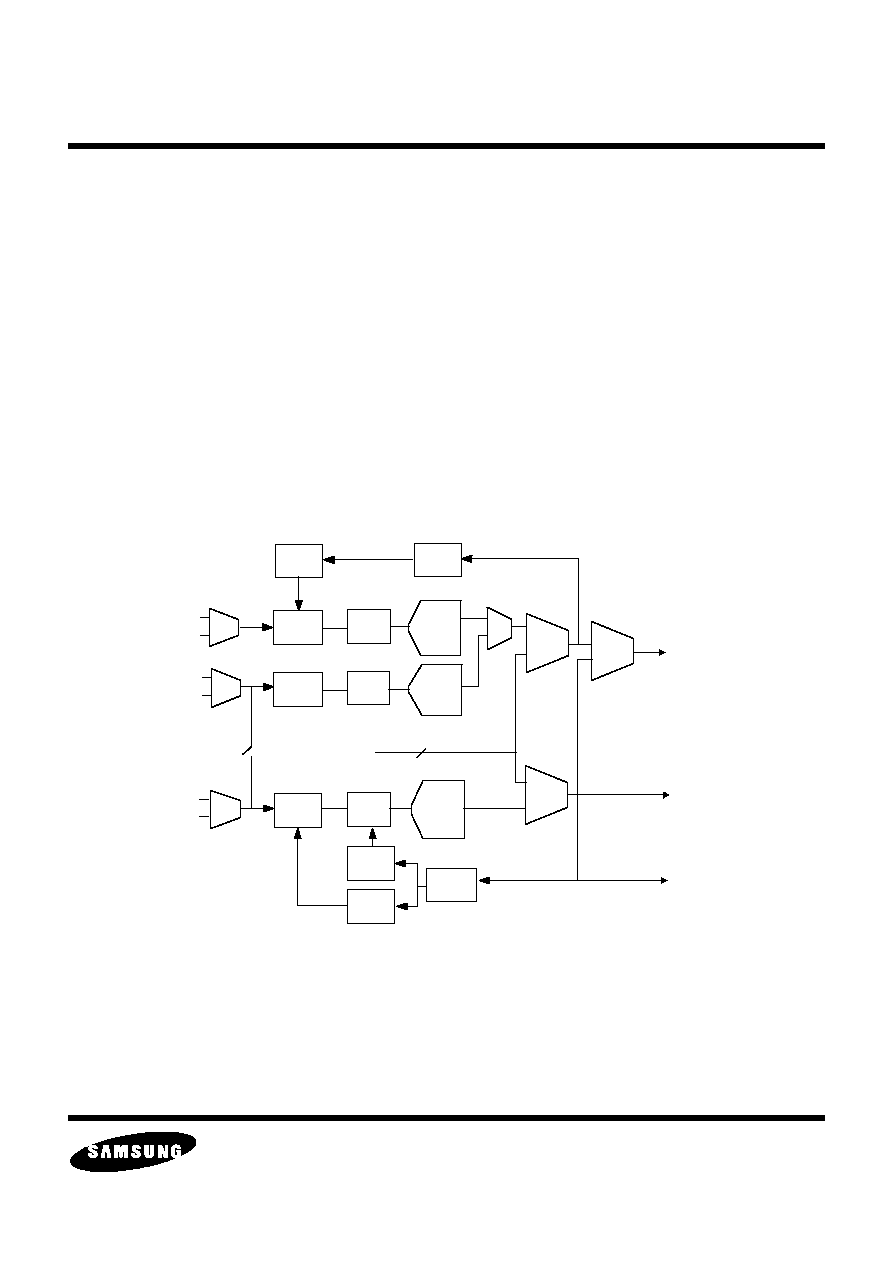
Figure 1 shows the detailed block diagram of the analog front end. Up to four composite video sources, two
S-video sources, two 3-wire YPbPr component video source, or any combination can be selected. The allowed
inputs are selected using the INSEL[2:0] bits in the CMDB register. Table 1 lists all possible input selections. The
front end has three paths each containing an analog gain control, a clamping control, and an 8-bit ADC. Composite
video input uses only the luma path. The ADC digital data is used to calculate the correct gain and clamp values.
The data is
feedback to the analog clamping and gain control. This architecture eliminates any offset and gain
mismatch in the analog front end.
Figure 1. Analog Front End
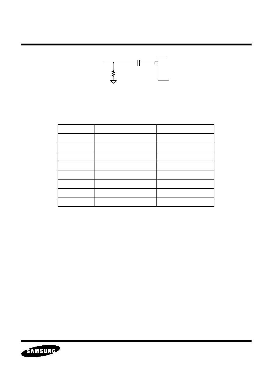
The analog inputs must be AC coupled through an external 0.1 mF capacitor clamp. Due to the high sampling rate
of the ADC's inside the S5D2650, most video sources will not require a low-pass filter for alias reduction. For those
video sources with harmonics above 13 MHz, a simple single order pole at 6 MHz will provide sufficient high
e
q
{
e
cie
{
cie
e
cfe
{
cfe
nrh
nrh
eektXWX
eektXWX
gP x
Z
q
P
q
P
i
P
e
q
e
cie
e
cfe
exduSQ{S
exduRQ{R
eS
eR
exduTQeR
exduUQeS
v n
r
v e
r
v v
i
exdu
ELECTRONICS
S5D2650 Data Sheet
MULTIMEDIA VIDEO
PAGE 9 OF 95
7/18/03
frequency signal reduction. This can be implemented with a 400 pF capacitor in parallel with the 75
load.
Figure 2. Typical Analog Video Input
1.1.2. Digital AGC Control
The AGC normally references to the ADC code difference between sync tip and back porch. Two sets of sync
tip-back porch ADC values are available for different AGC gain requirements: if AGCGN = 0, the sync tip locks to
code 2, and the back porch locks to code 70; when AGCGN = 1, the sync tip locks to 16, and the back porch locks
to code 70. Video signal with abnormal sync tip or very bright saturated colors may cause the ADC to limit the
maximum value. This situation can be corrected by enabling the AGCOVF bit in the CMDB register to force the
gain tracking loop to reduce AGC when maximum limiting conditions occur. The AGC may also be programmed to
freeze the AGC at the current value by setting the AGCFRZ bit in the CMDB register. Once the AGC is frozen, the
gain can be manually adjusted with the AGC register. The tracking time constant for the AGC can be controlled
with the AGC_LPG[1:0] bits in the TRACKB register. In addition, the AGC tracking time constant can be
configured as 2X faster during acquisition via the AGC_LKG.
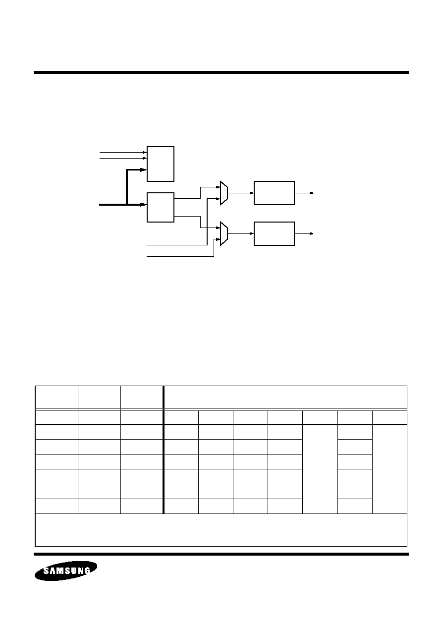
1.1.3. Digital Video Input
The high quality digital video down scaler in the S5D2650 can be directly accessed via the EXV bi-directional port.
The S5D2650 accepts CCIR 656 compliant 8-bit YCbCr digital video input with embedded or external HS, VS
timing. Video timing may also be generated by the S5D2650. Data path for 8-bit YCbCr input is shown in Figure 3.
Selection of analog video input or digital CCIR 656 data is with the INPSL[1:0] register bits.
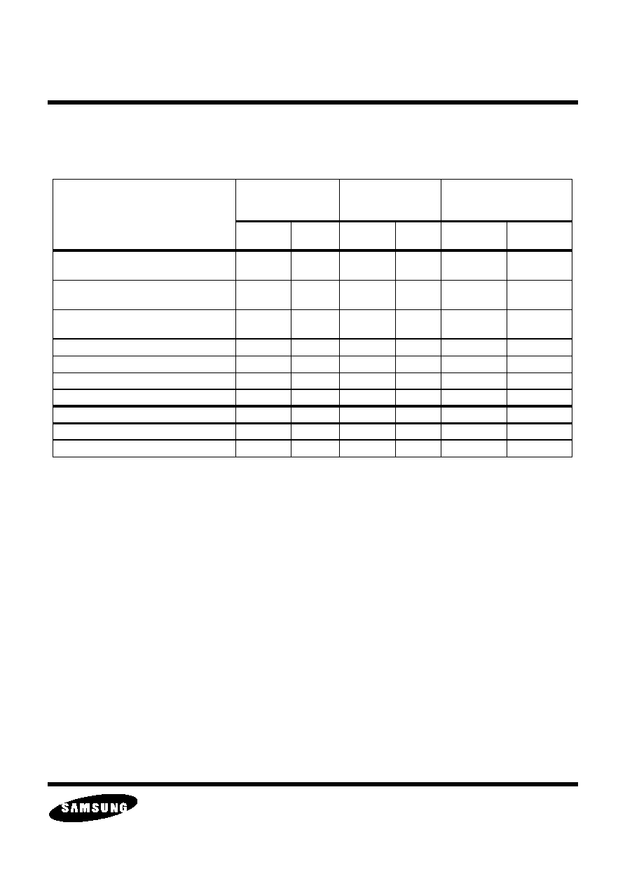
Table 1: Analog Video Input selections
INSEL[2:0](hex)
Selected Input(s)
Video Type
0
AY0
Composite
1
AY1
Composite
2
ACR0
Composite
3
ACR1
Composite
4
AY0,ACB0
S-Video
5
AY1,ACB1
S-Video
6
AY0,ACB0,ACR0
YPbPr component video
7
AY1,ACB1,ACR1
YPbPr component video
75
0.1
µ
F
Analog
Video
S5D2650
ELECTRONICS
S5D2650 Data Sheet
MULTIMEDIA VIDEO
PAGE 10 OF 95
7/18/03
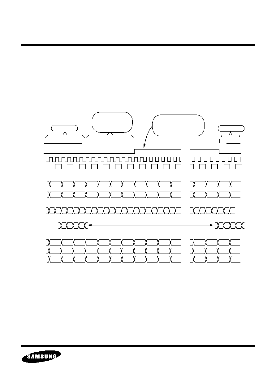
1.1.4. Pixel Clock and Timing Mode Selection for Digital Video Input
Pixel clock and synchronization timing can be individually selected to either come from an external generator or be
generated internally. In addition, if synchronization is provided by an external source, the S5D2650 supports
embedded syncs as defined in CCIR 656, or TTL HS and VS inputs. Selection of pixel clock is via CKDIR bit in
CMDD register. Timing selection is through either SYNDIR or EAV bit.
Figure 3. 8-bit YCbCr Input Data Path
By using an external pixel clock, the reference clock input at XTALI is no longer required. Additional register bits
have to be programmed for different selections of pixel clock and timing, which are detailed in Table 2. The
following register/bit-settings are required for digital video input:
INSEL[2:0] = 6,7 TSTCGN = 1. DMCTL[1:0] = 2 or 3. UGAIN = 238.
BRT = 34. SAT = 229. RGBH = UNIT = PED = 1.
Table 2: Digital Video Input Pixel Clock and Timing Selection
Pixel Clock TTL Timing
Embedded
Timing
Additional Register Programming
CKDIR
*1
SYNDIR
*2
EAV
*3
VMEN
TSTGPH TSTGEN TSTGFR
PIXSEL
MNFMT
IFMT
0
0
0
1
0
1
3
0 if input
data is at
square
pixel
rate.
1 if input
is at
CCIR
601 rate.
1
0 if input
is 50 Hz
video.
1 if input
is 60 Hz
video.
0
0
1
0
1
1
3
1
0
1
0
0
1
1
1
1
1
0
0
1
0
1
3
1
1
0
1
0
1
1
1
1
1
1
0
0
1
1
1
1
*1
: CKDIR = 0 - CK is output and is internally generated. CKDIR = 1 - CK is input from an external source.
*2
: SYNDIR = 0 - HS1 and VS are output. SYNDIR = 1 - HS1 and VS are inputs from external sources.
*3
: EAV = 0 - chip will not sync to embedded timing. EAV = 1 - chip will sync to embedded timing.
HS1
VS
EXV[7:0]
Timing
Control
Data
Demux
Y
C
Luma
Processing
Chroma
Processing
From Luma ADC
From Cb/Cr ADC
To Luma Scaler
To Chroma Scaler
ELECTRONICS
S5D2650 Data Sheet
MULTIMEDIA VIDEO
PAGE 11 OF 95
7/18/03
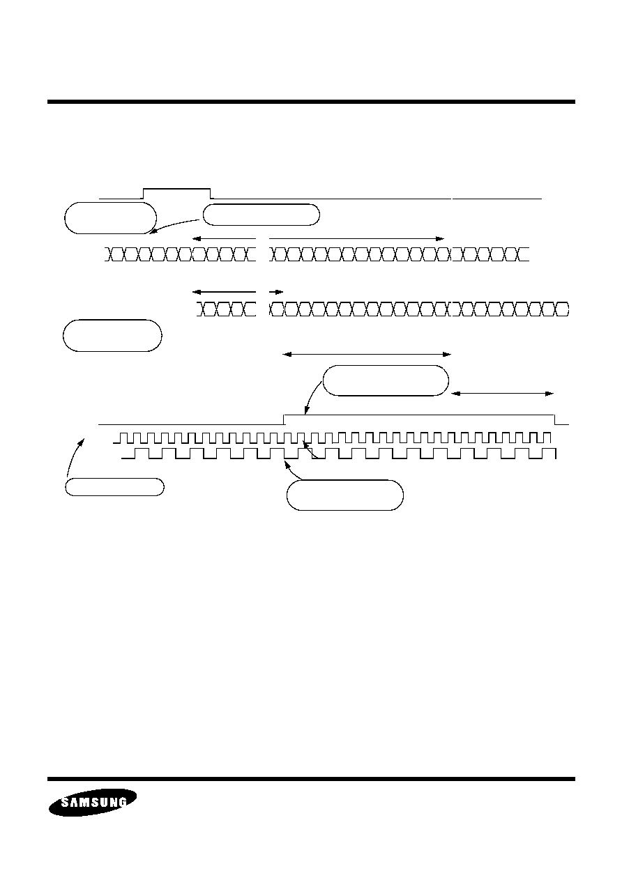
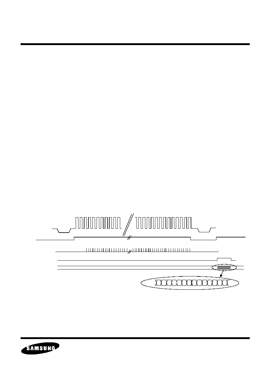
When in digital input mode, all programmable timing registers (such as HAVB,HAVE, HS2B etc.) are still functional.
If HS1 and VS are programmed as inputs, the associated output timing controls such as HS1B,E will have no
effect. An example of horizontal timing for digital input is shown in Figure 4.
Figure 4. Horizontal Timing for EXV Port as Digital Input
1.1.5. Additional Information for Analog Component Video Input
For the S5D2650 to correctly set the V component phase in PAL mode analog component video input mode,
PORTA (pin 58) need to be connected VSS. PORTA has to be configured as input (DIRA = 0) and connected to the
internal CBG signal (DATAA[2:0] = 3). Also S5D2650 supports progressive analog component input.
The following registers are required for analog component video input:
INSEL[2:0] = 6,7 PROG = 0(interlace), 1(progressive).
DATAA[2:0] = 3. CKILL[1:0] = 2. CDMLPF = 1.
SAT[7:0] = 79.
MNYCMB = 1. YCMBCO[2:0] = 4.
TSTCGN = 1. UOFFST[5:4] = VOFFST[5:4] = 3.
UOFFST[3:0] = C. VOFFST[3:0] = 2. VGAIN[7:0] = 1D. DMCTL[1:0] = 2 or 3
80 10 80 10 80 10 U
0
Y
0
V
0
Y
1
U
2
Y
2
V
2
Y
3
U
4
Y
4
V
4
Y
5
U
6
Y
6
V
6
Y
7
U
x
Y
x
V
x
Y
x
U
x
HAV
CK
CK2
HS1
80 10 80 10 80 10 U
0
Y
0
V
0
Y
1
U
2
Y
2
V
2
Y
3
U
4
Y
4
V
4
Y
5
U
6
Y
6
V
6
Y
7
U
x
Y
x
V
x
Y
x
U
x
Y
x
V
x
Y
x
V
x
Programmable, when an
Fully programmable HAVB location
HAV -- fully programmable,
Defines location of first, last pixel
and defines Cb,Y,Cr data location
Data group delay through chip --
EXV[7:0]
output - Any input phase
is acceptable
Constant to internal counter reference
based on internal counter
Fully programmable
HAVE location
The CK2 output clock phasing
is aligned to the HAV leading
edge
CK can be input or output
This HS1 location can also come
From a 656 SAV code
Y[7:0]
Y output for OFMT=2 is
shown, any 8 or 16 bit
output format is allowed.
ELECTRONICS
S5D2650 Data Sheet
MULTIMEDIA VIDEO
PAGE 12 OF 95
7/18/03
1.2. VIDEO TRACKING AND TIMING GENERATION
When the S5D2650 is configured for analog video input, the chip tracks the video input and generates a sampling
clock that is line locked to the input video. The S5D2650 requires an external reference clock for video tracking.
This reference can be supplied via a crystal using the on chip crystal interface or any TTL compatible source.
These configurations are shown in Figure 5
1.2.1. Clock Input Timing Reference
The S5D2650 can use either a 24.576 MHz or a 26.8 MHz reference. However, it is recommended that the 24.576
MHz reference be used for CCIR 601 operation, and the 26.8 MHz reference be used for square pixel or dual mode
operation. Other specifications for the crystal are:
· Fundamental or third overtone
· Load capacitance of ~20 pF
· Series resistance of 40
or less
· Frequency deviation of 50 ppm or less over operating temperature range
Figure 5. Standard Clock Configurations
1.2.2. The Sampling Clock
The sampling clock is generated by multiplying the line rate by N. This ensures that samples are aligned
horizontally, vertically and in time. The required N factor for the S5D2650 is based upon the field rate (60 Hz or 50
Hz) and the desired sampling rates (CCIR 601 or square pixel). Field rate can be automatically detected and can
be monitored with the FFRDET bit in the STAT register. Manual control of the field rate can be controlled with the
MNFMT and IFMT bits. The PIXSEL bit in register CMDA
selects CCIR 601 or square pixel. Table 3 shows the
constants for the various combinations of input formats and output pixel rates.
Using a Crystal
S5D2650
7
8
Using a Clock
24.576 MHz
TTL Clock
24.576 MHz
22 pF
22 pF
N. C.
XTALI
XTALO
S5D2650
7
87
XTALI
XTALO
391 pF
5.7
µ
H
Optional for 3rd
harmonic crystal
ELECTRONICS
S5D2650 Data Sheet
MULTIMEDIA VIDEO
PAGE 13 OF 95
7/18/03
The time constants for the pixel clock tracking loop can be adjusted with the HFSEL[1:0] bits.
In addition to providing the pixel clock, the S5D2650 also outputs various timing signals to indicate the beginning of
a line, a field, and for field and frame identification. All the timing and clock pins may be optionally put into high
impedance state. Tri-state of these pins are software controlled and initial state of these pins at power up is
controlled via two configuration pins: 3 and 4.
The S5D2650 can generate all the video timing without video input. This enables the S5D2650 to be used as a
video timing generator for a system that contains both the S5D2650 for live video input and a MPEG decoder
which requires a video timing generator.
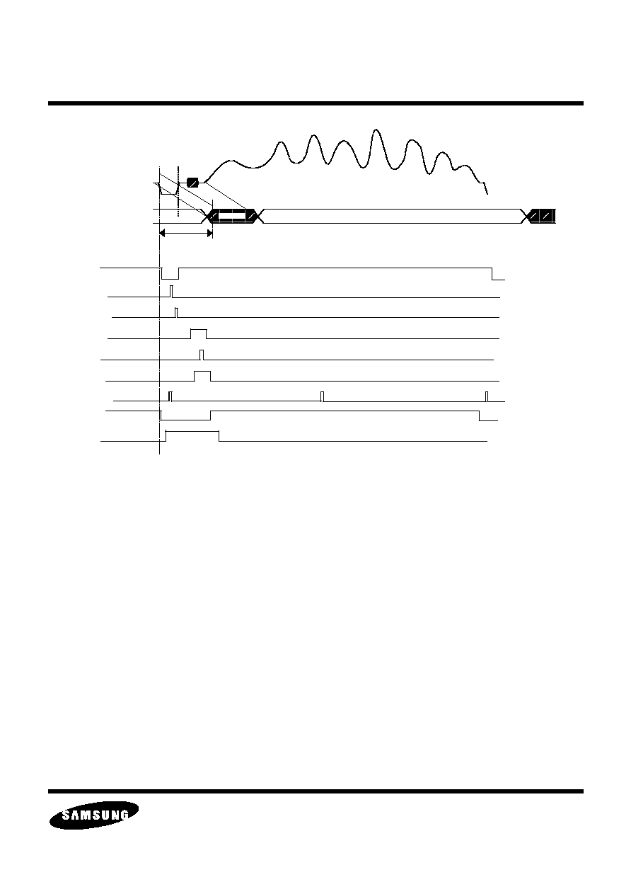
1.2.3. Horizontal Timing
The S5D2650 creates many internal timing signals aligned to the horizontal sync tip (mid-way of the falling edge of
horizontal sync, typically ADC code 36). These include locations of color burst (CBG, CBGW) used in chrominance
processing, back porch (BPG), and sync tip timing signals (SLICE, FS_PULSE) used for AGC and clamp functions.
SLICE is low whenever the input is below half way level of horizontal sync (typically ADC code 36). FS_PULSE is
a single clock pulse coincide with the start of SLICE. One of these internal signals can be made available at the
PORTA or PORTB pin at any time.
The chip outputs two horizontal synchronization signals: HS1 and HS2. The start and stop locations for these
signals are fully programmable. Offset programmed to HSxB, HSxE, and HSxBE0 are added to the default edge
locations as shown in Table 4. Note that there are different modulo numbers for different input video standards and
output pixel rates
.
Table 3: Timing for Different Pixel Rates
CCIR 601 Data Rates
Square Pixel Data Rates
Units
M
N,B,G,H,I,D,K,K1,L
M
N,B,G,H,I,D,K,K1,L
Field Rate
60
50
60
50
Hz
Pixels/Line (N)
858
864
780
944
Pixels
Active Pixels/Line
720
720
640
768
Pixels
Active Lines/Frame
480
580
480
580
Lines
Pixel Rate
13.5
13.5
12.27
14.75
MHz
ADC Sampling Rate
27
27
24.54
29.5
MHz
ELECTRONICS
S5D2650 Data Sheet
MULTIMEDIA VIDEO
PAGE 14 OF 95
7/18/03
An additional signal, HAV, is provided for horizontal video cropping. This signal has programmable polarity, start
and stop locations. Two 11-bit registers, HAVB and HAVE, are used to define the first and last pixel locations of the
horizontal portion of the cropped video. Numbers programmed into these registers are used as offset to the default
locations as shown in Table 4. Note that even though HAVB and HAVE have 1-CK resolution, the difference
between them should be maintained at multiple of 4 CKs for correct output.
Table 4 shows the default edge locations relative to the midway of the falling edge of the analog horizontal sync.
Note the numbers shown are in multiple of CK clocks. Figure 6 shows the approximate locations for the horizontal
timing signals.
Table 4: Horizontal Timing Signal Edge Locations (in # of CK)
Description
Signal
60 Hz
50 Hz
CCIR 601
(modulo 1716)
Square Pixel
(modulo 1560)
CCIR 601
(modulo 1728)
Square Pixel
(modulo 1888)
Chip delay
120
120
120
120
Sync gate (1-CK pulse)
SYG
72
72
72
72
Back porch gate
BPG
[157 232]
[139 214]
[164 244]
[178 264]
Color burst gate (1-CK pulse)
CBG
222
204
234
254
Wide color burst gate
CBGW
[159 254]
[147 233]
[173 254]
[186 277]
Two pulses per line (1-CK each
pulse)
FH2
40, 900
42, 822
42, 906
42, 986
Chrominance offset duration
COFF
[72 232]
[72 214]
[72 244]
[72 264]
Default horizontal sync(int.)
HS1
[24 222]
[24 204]
[24 234]
[24 254]
Default horizontal active(int.)
HAV
[293 17]
[276 0]
[321 33]
[357 1]
ELECTRONICS
S5D2650 Data Sheet
MULTIMEDIA VIDEO
PAGE 15 OF 95
7/18/03
Figure 6. Approximate Locations for the Horizontal Timing Signals
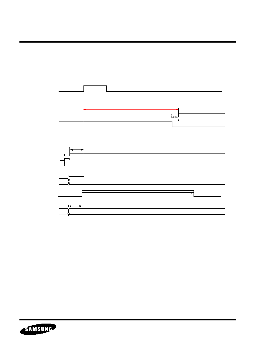
1.2.4. Vertical Timing
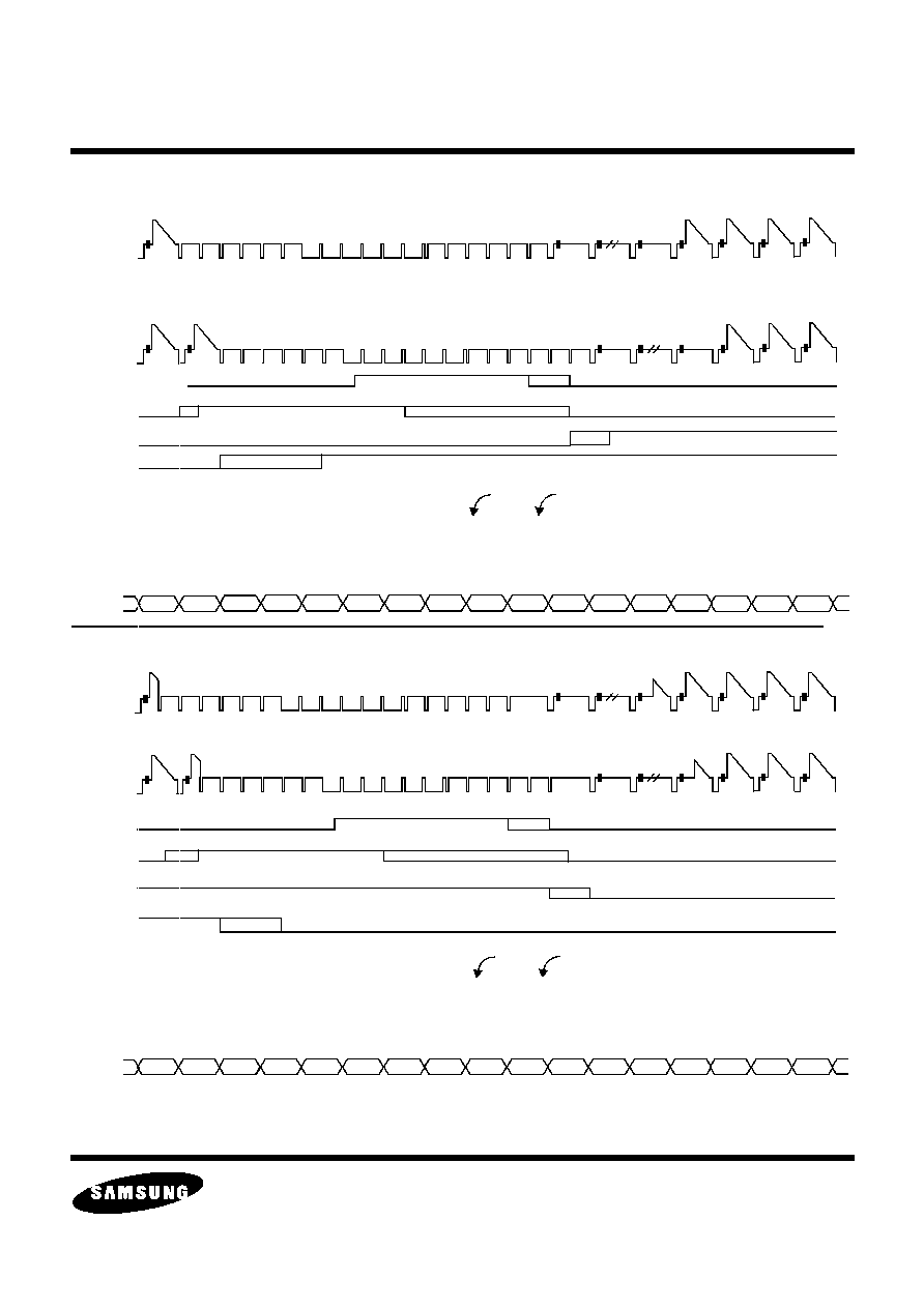
The vertical timing signals include VS, VAV, ODD, SCH, and PID.The VS is used for identifying the first line of video
in the vertical position. The VS leading edge can be programmed to either track the incoming video's serration
pulses or to be aligned to the beginning of the video line or half way, as shown in Figure 36 and Figure 37. If
VALIGN = 0, the VS leading edge is based on the output of an internal low pass filter, and its location is dependent
on the noise conditions of the video input. The trailing edge of VS is locked to either the beginning of the video line
or half way. The half way location relative to the beginning of the video line changes depending on current input
standard and output format. If VALIGN = 1, the leading edge of the VS is aligned to the beginning of the video line
or half way. The trailing edge is always aligned to the beginning of the video line. The VSE bit in the CMDA register
can be programmed to shorten the VS falling edge by one horizontal line.The VAV signal is used for vertical
cropping. The start and stop lines for VAV are programmable through the VAVB and VAVE registers,
respectively.The ODD signal signifies the current field number. When ODD is active, the current field is 1 or 3 (or 5
or 7 if in PAL mode). The leading and trailing edges of ODD can be aligned to either the leading edge of VS
(VALIGN = 1) or the trailing edge of VS (VALIGN = 0). The signal may be used in conjunction with SCH and PID to
exactly identify the current field. To distinguish between fields 1, 2 verse fields 3, 4 (or fields 1, 2, 3, 4 verse fields 5,
6, 7, 8 for PAL) the phase of the color burst relative to the sync tip must be measured. That information is provided
by the PORTB(SCH) pin. The S5D2650 provides the output of a comparator that measures whether the current
color burst phase relative to the falling edge of the sync is greater or less than a predetermined constant. This
constant is controlled with SCHCMP[3:0]. The polarity of the SCH output pin depends on the current
Digital video output
HS1,2
HAV
Blank
Active video
Active video
Analog video input
Chip delay
FS_PULSE
SLICE
SYG
BPG
CBG
CBGW
FH2
ELECTRONICS
S5D2650 Data Sheet
MULTIMEDIA VIDEO
PAGE 16 OF 95
7/18/03
SCHCMP[3:0] value. The SCH signal changes every video line. The SCH for line 260 is held for the entire vertical
blanking period. By using the SCH signal for the same line from each field, proper field identification can be
determined. Figure 8 shows field identification values for SCHCMP[3:0]=0. It is important to note that the SCH
value is only valid for video signals that have a constant sync tip to color burst relationship. This is not the case with
consumer VCRs.
.
Figure 7. Short Term Vertical Timing
HS1
VS
ODD
VAV
EVAV
(default)
ODD FIELD and VALIGN = 0
60 Hz - CCIR 601 = 885, Square = 708
50 Hz - CCIR 601 = 891, Square = 971
0, except 60 Hz Square = 2
EVEN FIELD or VALIGN = 1
27, except 60 Hz Square = 28
0, except 60 Hz Square = 2
VS
ODD
Note: Numbers shown are in CK. Active high polarities are used. Timing shown for VAV and EVAV are with qualifier off.
15, except 60 Hz Square = 14
60 Hz - 261
50 Hz - CCIR 601 = 273, Square = 341
HAV
default width for each input standard and output mode
ELECTRONICS
S5D2650 Data Sheet
MULTIMEDIA VIDEO
PAGE 17 OF 95
7/18/03
Figure 8. NTSC Vertical Timing Signals
The PID pin is used to identify whether the current V-axis is inverted in PAL mode. This signal changes at the color
burst. By noting this value at the same line of each field, a determination of whether a field is from {1-4} or {5-8} can
be made. As with the SCH pin, the S5D2650 is designed to hold the line 260 PID measurement for the entire
vertical blank period. This allows easy sampling of the PID or current field identification.
The ODD, SCH and PID signals change at different times and more than once within the video fields. Proper data
for field identification is determined by latching all three signals at the trailing edge of VS. Figure 9 shows the VS,
ODD, SCH, and PID signals and their latched values for each of the 8 possible fields. Figure 10 is the line to line
timing diagram for these signals in PAL mode.
Figure 9. PAL Vertical Timing Signals
VS
ODD
SCH
1
2
3
4
FIELD
ODD
SCH
1
2
3
4
H
L
H
L
H
L
L
H
Truth Table
Note:
ODD and SCH are
measured at the trailing
edge of VS.
VS
ODD
SCH
1
2
3
4
FIELD
ODD
SCH
1
2
3
4
H
L
H
L
H
L
H
L
Truth Table
Note:
ODD, SCH and PID are
measured at the trailing
edge of VS (VALIGN = 0).
5
6
7
8
PID
5
6
7
8
H
L
H
L
L
H
L
L
PID
H
L
L
H
H
L
L
H
ELECTRONICS
S5D2650 Data Sheet
MULTIMEDIA VIDEO
PAGE 18 OF 95
7/18/03
Figure 10. Line to Line VS, SCH and PID Timing (PAL input)
1.3. HORIZONTAL LUMA PROCESSING
A simplified block diagram for the luma path is shown in Figure 11.
Figure 11. Horizontal Luma Processing Unit
1.3.1. Luminance DC Gain
The S5D2650 can accommodate CCIR 624 M/N/H/G standards, which fall into categories of -40 or -43 sync tip and
inclusion or exclusion of 7.5 setup. The S5D2650 can produce correct CCIR 601 luminance output levels by
controlling the gain and offset in the luminance path via PED. This register should be set for the appropriate input
standard. The programmable CONT and BRT registers provide the user with additional flexibility to create
non-standard luminance gain and offset values.
ODD
PID
VS
HS
SCH
Decimation
Filter
Chroma
Trap
HYBWR
CTRAP
HYPK
CONT
BRT
FROM ADC
Horizontal
Peaking
Contrast
Control
Brightness
Control
Programmable
Low Pass Filter
HYLPF
HYBWI
ELECTRONICS
S5D2650 Data Sheet
MULTIMEDIA VIDEO
PAGE 19 OF 95
7/18/03
Figure 12. Luminance Signal
Luminance levels produced by the S5D2650 for different broadcast standards (assuming AGCGN=0, CONT=0 and
BRT=0) are summarized in Table 5.
When digital component output is desired in RGB mode, the RGBH register can be programmed to increase the
0-100% values from standard CCIR 601 levels to full range levels.The gain variations are shown in Table 6.
Table 5: Luminance Digital Level Code
M/N PED=1
M/N PED=0
B/G/H PED=1
Signal
Level
(IRE)
ADC
(CVBS)
Y[7:0]
Level
(IRE)
ADC
(CVBS)
Y[7:0]
Level
(IRE)
ADC
(CVBS)
Y[7:0]
Max Input
109
255
255
109
255
255
117
255
255
Peak White
100
240
235
100
240
235
100
229
235
Black
7.5
83
16
0
70
16
0
70
16
Blank
0
70
1
0
70
16
0
70
Sync
-40
2
1
-40
2
1
-43
2
S5D2650 Data
Path Equation
Table 6: RGB Output Range
RGB normal gain (RGBH=0)
RGB high gain (RGBH=1)
Signal
Cy
RGB (U,V=0)
Cy
RGB (U,V=0)
Peak White
235
235
255
255
Black
16
16
0
0
Peak W hite
B lack Level
B lanking Level
S ync Tip
M ax Input
C
Y
1.37 CV BS 100
=
A
{
SPTZZAN@K YV
=
A
{
SPUYAN@K ZR
=

ELECTRONICS
S5D2650 Data Sheet
MULTIMEDIA VIDEO
PAGE 20 OF 95
7/18/03
For CCIR 601 digital video input (INPSL[1:0] = 1), register UNIT must be set to 1 to produce unit gain.
1.3.2. Horizontal Luma Frequency Shaping
The luma path contains many programmable filters for different purposes. The combination of these filters will give
different frequency characteristics.
The over sampled video data from the ADC pass through a decimation filter. The decimation filter has user
programmable bandwidth. Three registers are used to control the decimation filter characteristics and each is
designed for certain purposes. The HYBWI, when set to "1", provides extra bandwidth for very high quality video
source. The HYBWR, when set to "1", reduces the bandwidth so high frequency noise can be eliminated. The 3-bit
register HYLPF[2:0] provides the necessary bandwidth reduction for horizontal scaling. When all three registers
are programmed to "0", the decimation filter has the bandwidth of the normal video. The S5D2650 provides the
option of bypassing the decimation filter. This option should be used only when the input video is band limited and
with low high frequency noise.
For composite video input, the notch filter can be enabled (CTRAP set to "1") to extract the luminance. The notch
filter has different center frequencies for different input video format. User selectable peaking function is included
for edge enhancement. The notch filter should be bypassed for S-video and component video input, or if luma
comb filter is enabled.
The luminance filter characteristics have been designed to be very similar for all combinations of 60/50 Hz video
and CCIR 601/square pixel sampling rates. Figure 13 and Figure 14 show the output characteristics of the
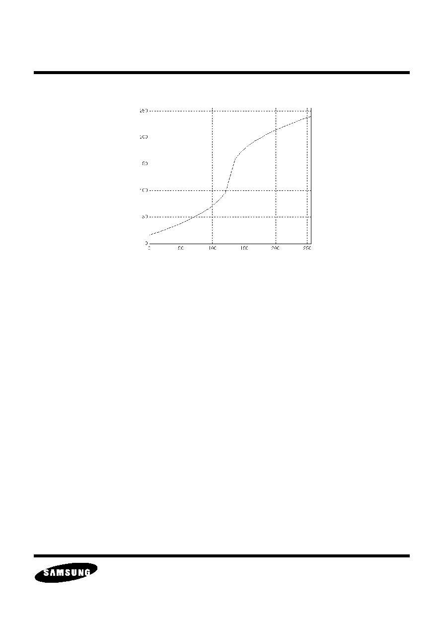
luminance path with different filter combinations for the supported input standards and output pixel rates.
ELECTRONICS
S5D2650 Data Sheet
MULTIMEDIA VIDEO
PAGE 21 OF 95
7/18/03
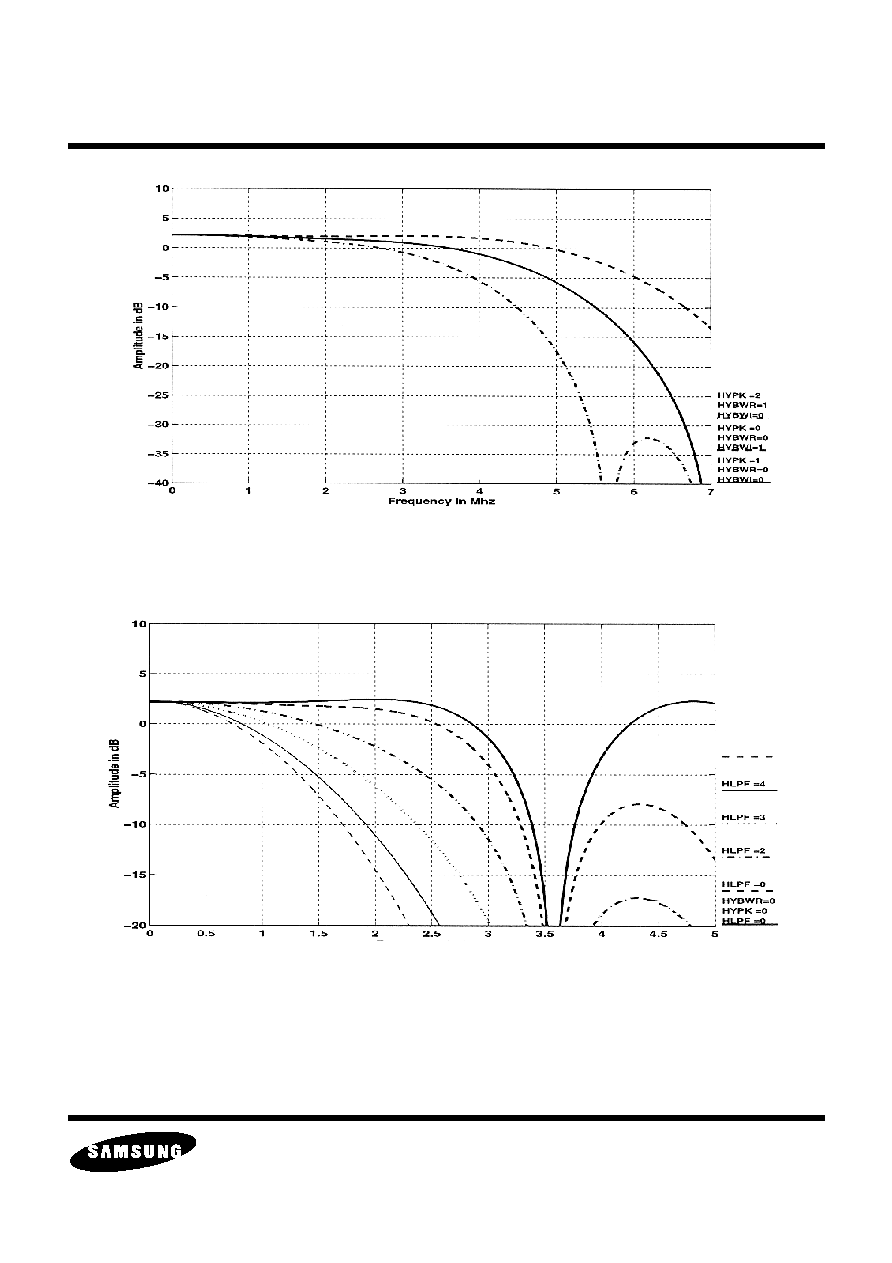
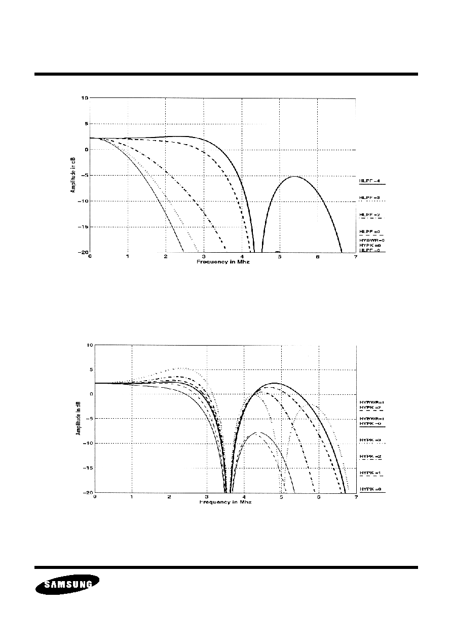
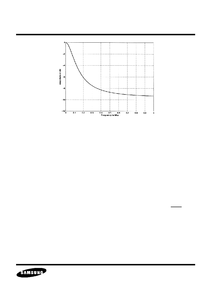
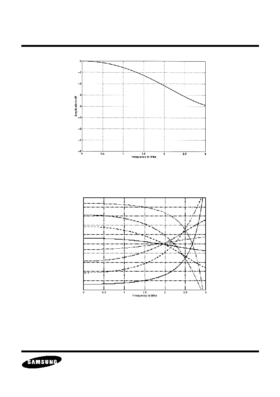
Figure 13. Medium to High Frequency Luma Filter Characteristics (CTRAP=0)
Figure 14. Medium to Low Frequency Luma Filter Characteristics (NTSC, CTRAP=1)
ELECTRONICS
S5D2650 Data Sheet
MULTIMEDIA VIDEO
PAGE 22 OF 95
7/18/03
Figure 15. Medium to Low Frequency Luma Filter Characteristic (PAL, CTRAP=1)
Figure 16. Luma Filter Characteristic with Peaking On (NTSC, CTRAP=1)
ELECTRONICS
S5D2650 Data Sheet
MULTIMEDIA VIDEO
PAGE 23 OF 95
7/18/03
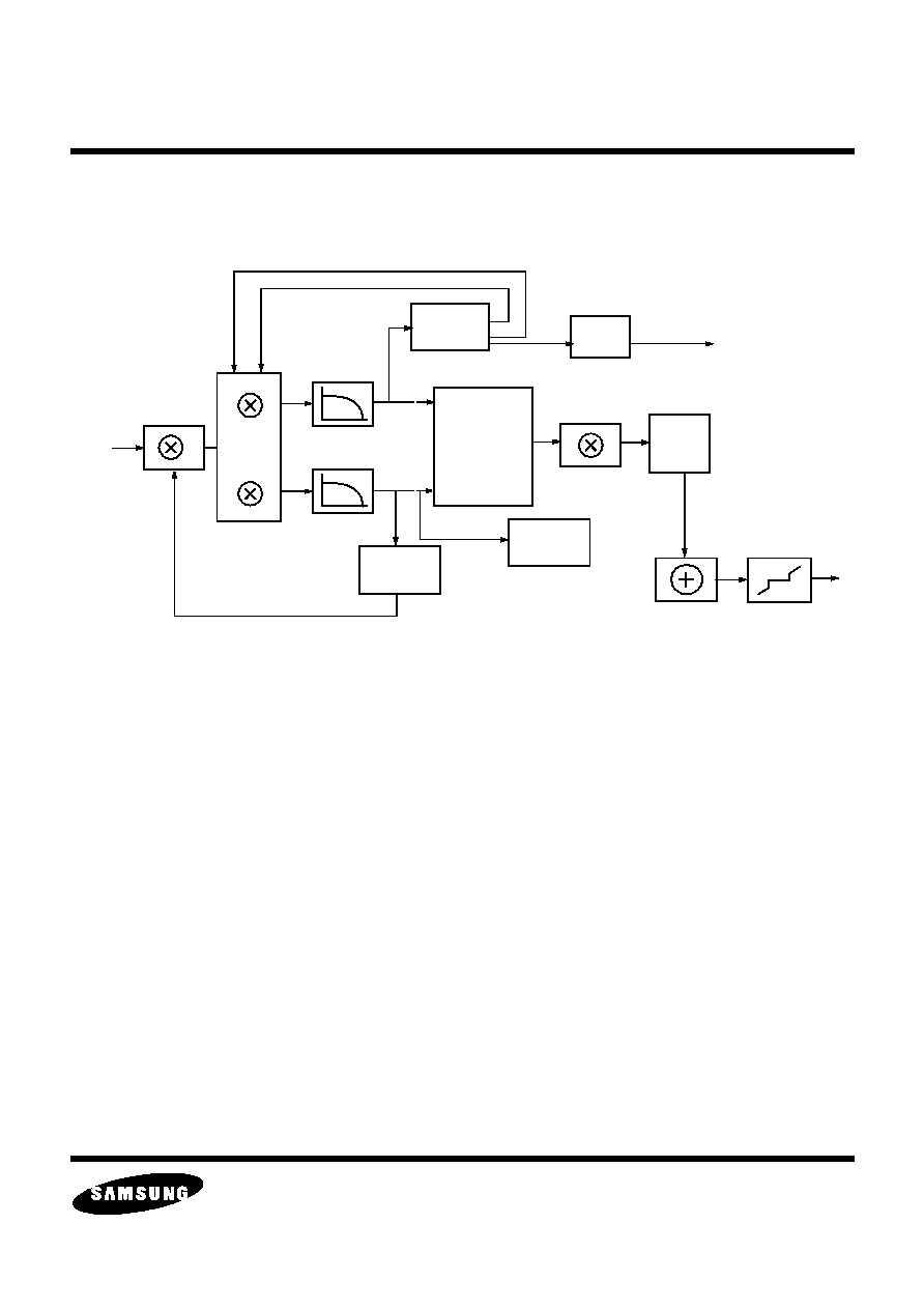
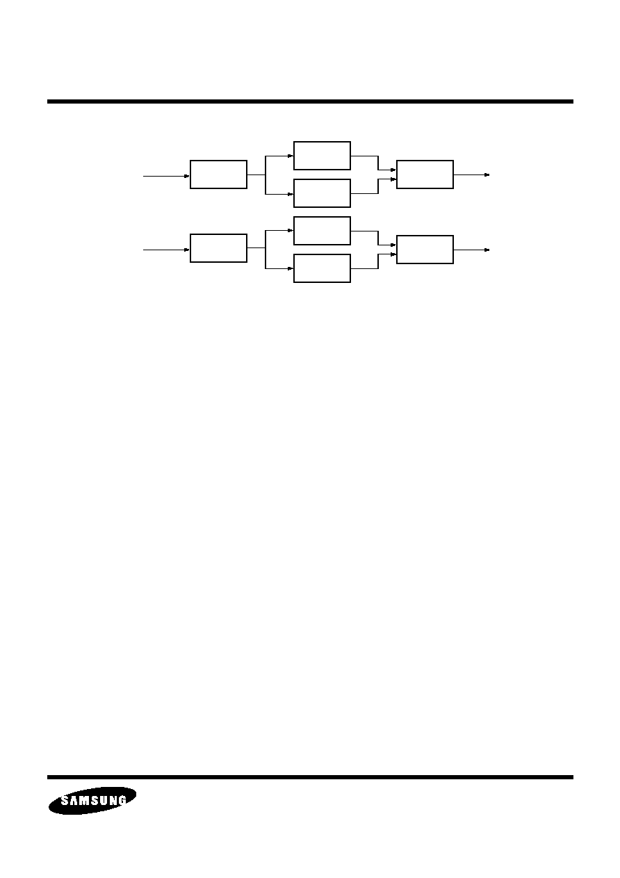
1.4. HORIZONTAL CHROMA PROCESSING
A simplified block diagram for the horizontal chroma processing unit is shown in Figure 17.
Figure 17. Horizontal Chroma Processing Unit
The S5D2650 supports chroma input in NTSC, PAL, SECAM and component formats. The color standard is
automatically detected and the various chroma processing blocks are enabled as required for the given chroma
standard. Details of the various chroma processing blocks follow.
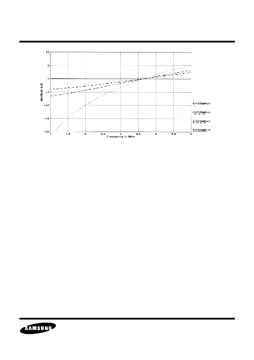
1.4.1. IF Compensation
For improved chroma demodulation when the input video is from a mis-tuned IF source, an IF compensation filter
is included that has variable gain for the upper chroma side band. This is controlled by the CIFCMP[1:0] bits at
location CDEM. The frequency response is shown in Figure 18. For convenience, all plots are normalized to the
NTSC modulation frequency.
Gain
Tracking
Frequency
Tracking
COS
V
U
SIN
CBW,FSEC
CBW,FSEC
CKILL
CGTC
SAT
CORE
HUE, TSTCFR
CFTC
Color
Killer
CKILL
Low
Pass
Low
Pass
FROM ADC
Saturation
Control
SECAM
Frequency
Differentiator
UGAIN
VGAIN
Coring
Control
UOFFST
Offset
Control
VOFFST
Gain / PAL
Control
Auto
Detect
RTCO
RTC_PID
RTC_DTO
Control
TSTCGN
ELECTRONICS
S5D2650 Data Sheet
MULTIMEDIA VIDEO
PAGE 24 OF 95
7/18/03
Figure 18. Chroma IF Compensation Frequency Response
1.4.2. Demodulation Gain
The demodulation gain block is controlled by feedback from the gain tracking block. For NTSC and PAL type
inputs, the gain constant is derived from a programmable reference compared against the U component of the
input video. This reference is controlled by the SAT register. The default value "0" is the correct gain (saturation for
nominal output). For SECAM type input, the feedback is calculated such that proper frequency demodulation is
obtained. When external calibration is desired, the gain feed back loop can be "opened" by setting TSTCGN=1.
The SAT then controls bits 8 through 1 of a 10 bit multiplier.
For standard auto tracking applications, it is recommended that the SAT register be used as an end user saturation
control. This register is 2's complement.
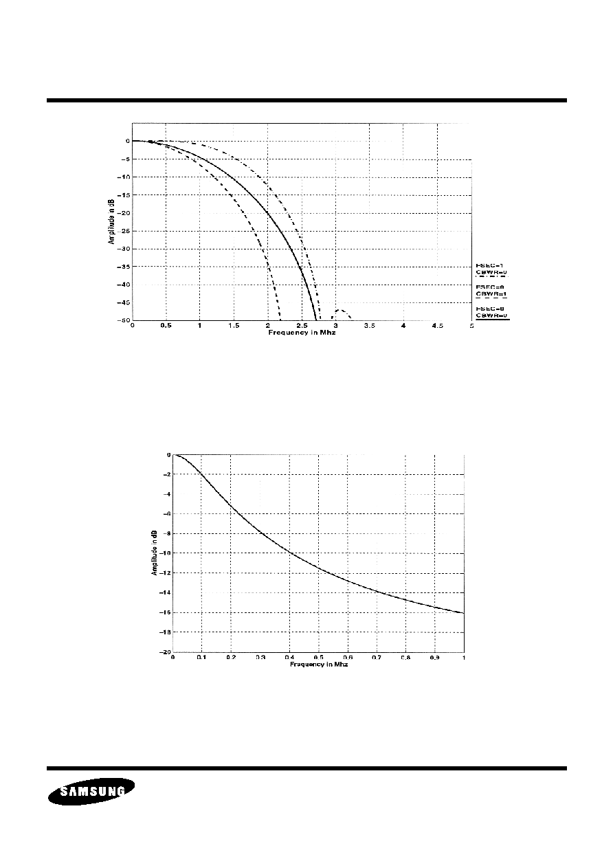
1.4.3. Demodulation Low Pass Filter
The demodulation circuit also contains a programmable low pass filter and a coring function for noise reduction.
The chroma low pass filter frequency response for the demodulation circuit for the various video standards are
shown in Figure 19
ELECTRONICS
S5D2650 Data Sheet
MULTIMEDIA VIDEO
PAGE 25 OF 95
7/18/03
Figure 19. Chroma Low Pass Filter Frequency Response
1.4.4. SECAM Demodulation
SECAM processing includes a frequency differentiator, a Cloche and a de-emphasis filter. Frequency response for
the filters are shown in Figure 20 and Figure 21.
Figure 20. Cloche Filter Frequency Characteristic
ELECTRONICS
S5D2650 Data Sheet
MULTIMEDIA VIDEO
PAGE 26 OF 95
7/18/03
Figure 21. De-emphasis Filter Frequency Response
1.4.5. Additional Chroma Functions
S5D2650 has many built in auto detection circuits. These allow S5D2650 to track any type of video standard input
automatically.
For analog component video input, the demodulation function is not enabled. The low pass filter provides a group
delay for Cb and Cr alignment. This enables the two components to be sampled by one ADC.
An RTCO serial output is provided that encodes the current chroma and pixel frequency of the decoder. This
information can be used by an Encoder running off of the decoder clock to produce proper color output. The
horizontal position of the serial signal is controlled by the HS2 location. The phasing of the DTO and the Encoder
can be reset using the RTC_DTO bit. For PAL mode, the PID polarity can be controlled with the RTC_PID bit.
1.5. COMB FILTER
Comb filters provide superior Y/C separation for composite NTSC and PAL than simple chroma trap filter. The
S5D2650 contains on-chip separate 2-line stored luma and chroma comb filters. An internal signal COMB controls
for what lines the comb function is enabled. This signal is available through the PORTB pin. Combing is part of the
vertical processing which also includes vertical scaling, which is discussed in Section 1.6. A block diagram for the
vertical processing section is shown in Figure 22.
ELECTRONICS
S5D2650 Data Sheet
MULTIMEDIA VIDEO
PAGE 27 OF 95
7/18/03
Figure 22. Vertical Processing
1.5.1. Luma Comb Filter
The luma comb filter reduces high frequency chroma leakage into the luminance path. The S5D2650 uses 2-line
stored luma data for combing. Filter coefficients for different video input standards are provided and can be
selected automatically based on the video input. Filter coefficients may also be set manually.
An optional active comb is employed for NTSC video. Selection of luma comb coefficients is based on line-to-line
chroma correlation.
Provision is made to disable luma comb for S-video, component, or digital video input. This is achieved by
programming the luma comb control register MNYCMB to "1", and by choosing the value 3 or 4 for YCMBCO[2:0].
This will result either a 1-line or 2-line luma delay. Care must be exercised when disabling the luma comb so that
luma line delay matches the chroma path line delay.
Special filtering is applied to ensure that high vertical bandwidth is retained for the luma path.
1.5.2. Chroma Comb Filter
The chroma comb filter provides further color separation from the composite video. Filter coefficients can be
automatically selected based on the input video standard or manually set using NMCCMB and CCMBCO[2:0].
Luma
Chroma
Horizontal
Scaler
Horizontal
Scaler
Luma
Adaptive
Comb
Chroma
Comb
Y
C
Luma
Vertical
Scaler
Chroma
Vertical
Scaler
Vertical
BW
Retention
Sum
ELECTRONICS
S5D2650 Data Sheet
MULTIMEDIA VIDEO
PAGE 28 OF 95
7/18/03
1.6. SCALING
The S5D2650 includes a high quality down scaler. The video images can be down scaled in both horizontal and
vertical direction to an arbitrary size.
1.6.1. Horizontal Scaler
The horizontal scaler uses a 5-tap 32-phase interpolation filter for luma, and a 3-tap 8-phase interpolation filter for
chroma. Scaled pixel data are stored in an on-chip FIFO so they can be sent out in a continuous stream.
Horizontal scaling ratio is programmed via the 15-bit register HSCL. The timing signal EHAV is used to indicate
when scaled pixel data is available at the video output port. EHAV can be programmed so that it is active for every
line regardless of vertical cropping and scaling. Or it can be programmed to be active only for valid video lines. For
example, Figure 23 shows the timing for CIF output assuming HAV is programmed to be active for 720 pixels. The
HSCL register is programmed with the value 4000 (hex). The trailing edge of EHAV is either aligned with the
trailing edge of HAV if the total number of scaled pixels is even, or is one pixel clock earlier if the number is odd.
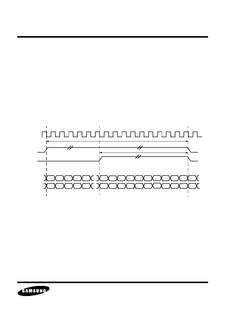
Figure 23. Horizontal Scaler Timing for CIF Output (CCIR 601 Pixel Rate)
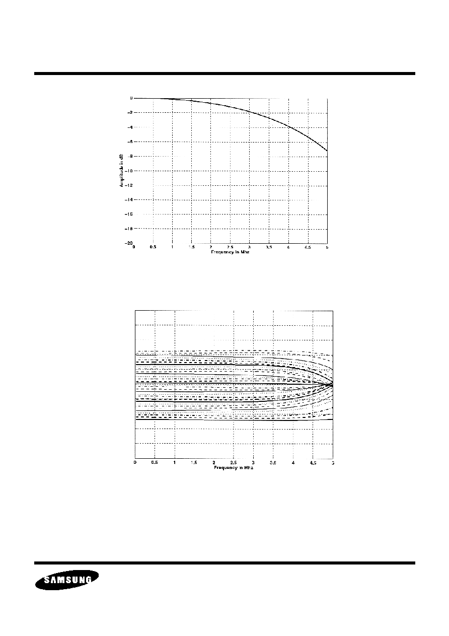
Frequency response and group delay for the luma scaler are shown in Figure 24 and Figure 25, respectively. The
luma interpolation filter is designed to achieve relatively flat frequency response and minimal group delay up to the
normal video bandwidth. A flat full data path frequency response may be obtained with the help of the luma
peaking control register HYPK[1:0]. The high quality filter ensures minimal artifacts for any scaling ratio.
CK2
HAV
EHAV
720
360
Y[7:0]
Y
1
Y
0
Y
2
Y
3
-
-
Y
357
Y
358
Y
359
C[7:0]
V
0
U
0
U
2
V
2
-
-
V
356
U
358
V
358
Y
356
U
356
ELECTRONICS
S5D2650 Data Sheet
MULTIMEDIA VIDEO
PAGE 29 OF 95
7/18/03
Figure 24. Horizontal Luma Scaler Interpolation Filter Frequency Response
Figure 25. Horizontal Luma Scaler Interpolation Filter Group Delay
Because of the limited bandwidth of the chroma data, a simpler interpolation filter is used for the horizontal chroma
scaler. The frequency response and group delay for this filter are shown in Figure 26 and Figure 27, respectively.
1
1.5
2
2.5
3
gr
oup de
l
a
y
(
1
3
.
5
M
H
z
C
l
oc
k
s
)
ELECTRONICS
S5D2650 Data Sheet
MULTIMEDIA VIDEO
PAGE 30 OF 95
7/18/03
Figure 26. Horizontal Chroma Scaler Interpolation Filter Frequency Response
Figure 27. Horizontal Chroma Scaler Interpolation Filter Group Delay
0.5
1.0
1.5
Gr
o
u
p
D
e
la
y
ELECTRONICS
S5D2650 Data Sheet
MULTIMEDIA VIDEO
PAGE 31 OF 95
7/18/03
1.6.2. Luma Vertical Scaler
Vertical luma scaling uses either a 3-tap or 5-tap 8-phase interpolation filter depending on the horizontal scaling
ratio.
Vertical scaling ratio is programmed via the 14-bit register VSCL. A valid scaled line is indicated by the timing
signal EVAV being active. The EVAV can be programmed to be internally gated by the VAV signal so it can only be
valid within the vertically cropped region.
Luma horizontal scaling can use either a 3-tap or a 5-tap interpolation filter depending on the horizontal scaling
ration. If the scaled horizontal line has less than or equal to 384 pixels, the 5-tap luma interpolation filter can be
turned on by programming the VRT2X bit to a "1". Otherwise, the VRT2X bit should be set to "0" and the 3-tap filter
be used.
The VYBW bit provides additional vertical bandwidth control for vertical scaling. Typically, when the vertical scaling
ratio is less than 1/2, this bit should be set to "1" to eliminate any aliasing effect.
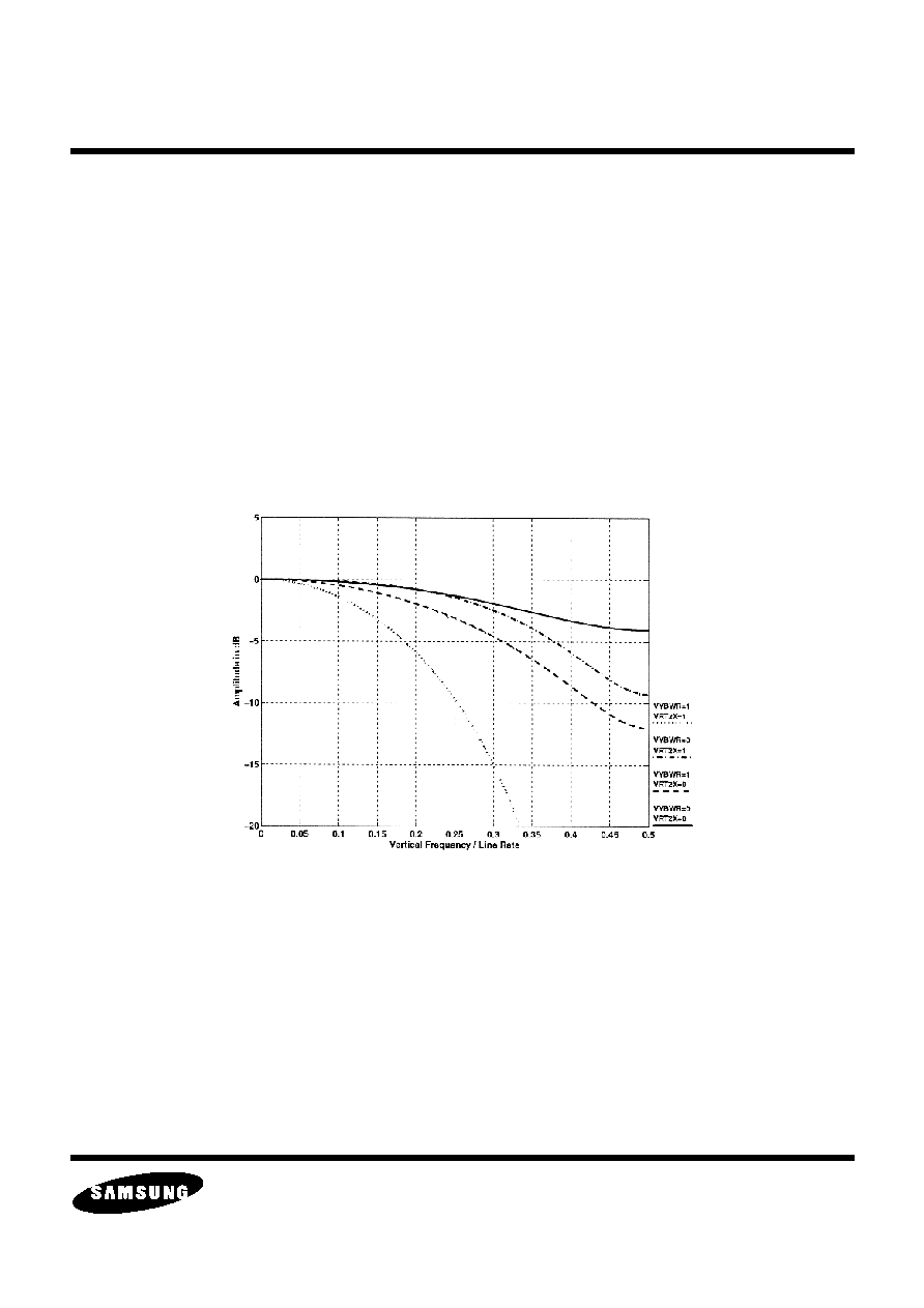
Luma vertical scaler interpolation filter frequency response is shown in Figure 28.
Figure 28. Luma Vertical Scaler Interpolation Filter Frequency Response
In vertical scaling, the start of signal VAV controls the phase of the vertical scaler interpolation filter. If VAVB, VAVE,
VAVOD0, VAVEV0, and VSCL are programmed such that the vertical interpolation filter has the same phase and
scaling ratio as that of a memory controller (most memory controller has simple line dropping vertical scaling), it is
possible to interface the S5D2650 to the memory controller without using EVAV.
1.6.3. Chroma Vertical Scaling
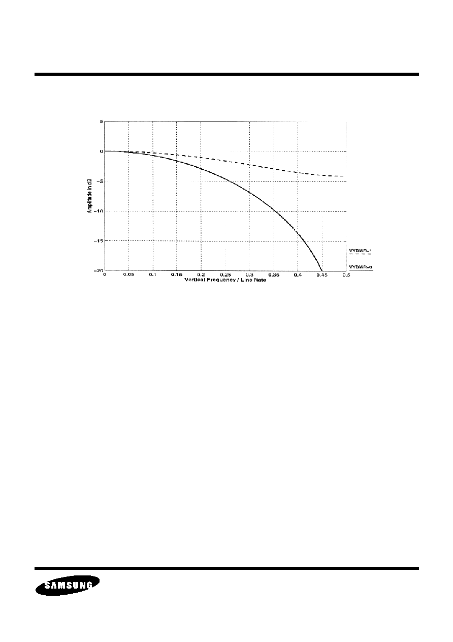
Chroma vertical scaling uses different algorithms depending on video input standard and horizontal scaling ratio. If
horizontal scaling results in line with less than or equal to 384 pixels, and the VRT2X is set to a "1", a 5-tap
interpolation filter will be used for all video inputs. Otherwise, for NTSC, a 3-tap interpolation filter will be used for
ELECTRONICS
S5D2650 Data Sheet
MULTIMEDIA VIDEO
PAGE 32 OF 95
7/18/03
NTSC input, and decimation (line dropping without filtering) will be used for PAL and SECAM. Filter characteristics
for the 3-tap and 5-tap filters are shown in Figure 29.
Figure 29. Chroma Vertical Scaler Interpolation Filter Frequency Response
ELECTRONICS
S5D2650 Data Sheet
MULTIMEDIA VIDEO
PAGE 33 OF 95
7/18/03
1.7. VBI DATA PROCESSING
The S5D2650 VBI data processing is very flexible in that it supports VBI data formats of:
· Closed Caption Line 21 Data Service (EIA-608)
· 525 line / 60Hz Teletext systems B,C,D (ITU-R BT.653-2)
· 625 line / 50Hz Teletext systems A,B,C,D (ITU-R BT.653-2)
· Copy Generation Management System (EIA/IS-702)
· Wide Screen Signalling (WSS ETS 300 294).
Note that the SMPTE data slicing is removed for the S5D2650 and replaced with the WSS / CGMS processing.
This data can be accessed from the part via four different methods:
· Enabling the "Raw un-processed 27MHz" Y ADC samples to be output for the appropriate lines in place of the
normal YUV data.
· Slicing the data (creating a clock and comparing the data to a threshold at the clock) and bursting this data out
on Y output.
· Reading the sliced data from two internal registers via the IIC bus.
· Via 2 external pins that output the sliced VBI data(CCDAT) and the time at which the slice is valid(CCEN).
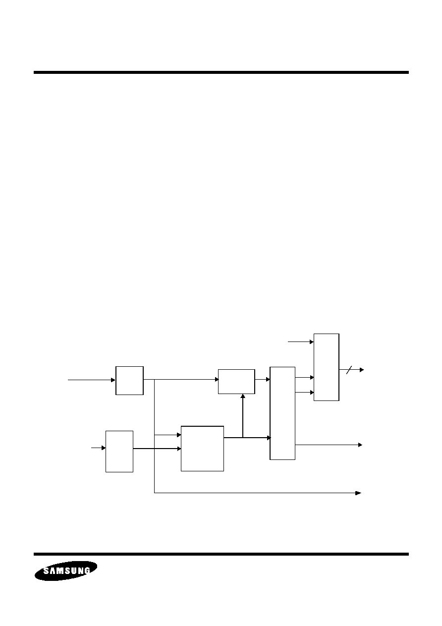
A simplified block diagram for the VBI section is shown in Figure 30.
Figure 30. VBI Decoder Block Diagram
MODE
CCEN
CLOCK
ODD
ODDEN
EVENEN
ODDOS
VBIL
CTRL
LOGIC
SLICER
From Y ADC
GENERATOR
PIXSEL
IFMT
SECAM
FRAME
ALIGNMENT
FIFO
8
Y[7:0]
Normal
Decoded Y Data
CCDATA
MUX /
VBI
Format
VYFMT
VBINSRT
TTFRAM
ELECTRONICS
S5D2650 Data Sheet
MULTIMEDIA VIDEO
PAGE 34 OF 95
7/18/03
Table 7 lists all the video standards that the VBI data slicer supports. Some of these modes are auto detected
based on the current video input standard,
Configuring the VBI processing consists of many different steps which are individually explained below.
1.7.1. Enabling the VBI Processor
The VBI processor can be enabled independently for the ODD or EVEN fields with the ODDEN and EVENEN bits.
Some VBI data is only present on line in 1 of the 2 fields, These independent field enables allow control of the total
VBI data output from the chip. These controls apply to all VBI Lines, Thus it is not possible to enable Closed
caption line 21 for the Even field and line 19 Teletext for both the odd and even field.
1.7.2. Selecting the Type of Output Data
As previously mentioned, there are 4 different ways the VBI data can be extracted. Three of these are selected as
shown in the table, the fourth method (CCEN and CCDAT pins) is always available if VBI processing is enabled.
Table 7: Video Standards Supported by VBI Decoder
Mode
Value of Chip
Detection Bits
Required Values of
Registers to enable
Standard
Characteristics of the
Standard
Format
SECAM
VBIL0-15 TT_SYS
Data Rate
(MHz)
Number of
Bits (bytes)
60Hz Teletext system C
(NTSC / Intercast)
1
0
2
0
5.727272
272 (34)
50Hz Teletext system B
(PAL)
0
0
2
0
6.9375
344 (43)
50Hz Teletext system A
(SECAM)
0
1
2
0
6.203125
304 (38)
60Hz Teletext system B
0
1
2
1
5.727272
280 (35)
50Hz Teletext system C
0
1
2
2
5.734375
272 (34)
50Hz Teletext system D
0
1
2
3
5.6457875
280 (35)
60Hz Teletext system D
0
1
2
3
5.727272
280 (35)
Closed Caption NTSC 601
N/A
N/A
1
N/A
0.5035
16 (2)
CGMS (NTSC 60Hz)
1
N/A
3
N/A
0.447443
20 (3)
WSS (PAL 50Hz)
0
N/A
3
N/A
5.0000
84
ELECTRONICS
S5D2650 Data Sheet
MULTIMEDIA VIDEO
PAGE 35 OF 95
7/18/03
The S5D2650 adds an additional output mode and flexibility to vary the modes from line to line. If VBCVBS=0 and
VBINSRT=1 S5D2650 will output sliced data on enabled lines. By setting VBIMID to 1, any line for which VBIL=3
will output raw ADC data instead of WSS or CGMS. This mode allows a mixture of sliced and raw data. This can be
used to output raw data from a teletext line and sliced data from a closed caption line.
1.7.3. Select Individual Lines Enabled for VBI Processing
The S5D2650 allows programmable selection of processing for the various video lines. For example
Teletext/Intercast data can be sliced for lines 14 - 17, and closed caption for line 21. Each 2-bit register VBIL0
through VBIL15 defines how a specific VBI line is processed. As can be seen in Figure 36 for 60 Hz and Figure 37
for 50 Hz video, the following alignments exist:
Table 8: VBI Data Output Mode (VBILn != 0)
VBCVBS
VBINSRT
Output Mode
0
0
The VBI data is available via the internal registers CCDAT1 and
CCDAT2. Only the last 2 extracted bytes are stored in these
registers. Thus, this mode is only useful for extraction of Closed
Caption data(Read the register value).
0
1
This mode enables output of the sliced VBI data(Y Port output).
1
0
This mode enables output of direct data from the ADC(ADC Data
bypass at 27Mhz sampling rate).
1
1
This mode is invalid.
Table 9: VBI Line(s) Selection
VBIL
number
Line Number That the VBIL Processing command applies
to (Assuming ODDOS=1)
Odd Field
60 Hz
Even Field
60 Hz
Odd Field
50 Hz
Even Field
50Hz
VBIL0
All Lines
Except 10-24
All Lines
Except
273-287
All lines
Except 7-21
All lines Except
320 - 334
VBIL1
9&10
272&273
6&7
319&320
VBIL2
11
274
8
321
VBIL3
12
275
9
322
VBIL4
13
276
10
323
VBIL5
14
277
11
324
VBIL6
15
278
12
325
VBIL7
16
279
13
326
VBIL8
17
280
14
327
VBIL9
18
281
15
328
VBIL10
19
282
16
329
VBIL11
20
283
17
330
VBIL12
21
284
18
331
VBIL13
22
285
19
332
VBIL14
23
286
20
333
VBIL15
24&25
287&288
21&22
334&335
ELECTRONICS
S5D2650 Data Sheet
MULTIMEDIA VIDEO
PAGE 36 OF 95
7/18/03
The ODDOS[1:0] bits allow offset between the odd and even fields. Thus VBIL9 can be lines 17,18 or 19 for ODD
fields while VBIL9 is still line 281 for EVEN fields. This extra controls account for variations of VBI data locations
from ODD and EVEN fields.
When Intercast or Teletext data is selected, an 8-bit user programmable register (TTFRAM) is provided for the
framing byte. The frame alignment processor uses this information to properly locate the first data bit on each line
1.7.4. Raw CVBS Data Output Format
When raw ADC data is selected as output in place of the normal YUV or RGB data. The following rules apply:
· For 656 type 8 bit outputs, The ADC data outputs with successive data points in place of the Cb, Y, Cr, Y data
stream.
· For 16 bit or 24 bit outputs, The ADC data is output on the Y[7:0] and C[7:0] output pins. At any CK2 clock 2
bytes of ADC data are output. The Y[7:0] bus represents data N while C[7:0] is data N+1.
· ADC data is only output during the region that HAV is active.
· All ADC outputs are limited to the range 1-254, thus a 0 or 255 value will not be output.
For the line selected mode described above using VBCVBS and VBIL, data is from the luma ADC only. If C ADC
data or the entire video line is required, configure OFMT bits.
1.7.5. Sliced Data Output Formats
While sliced data is available for many of the output formats, the target application is 656 output format. The
description of data format is limited to this mode. The S5D2650 allows this data to be output during active video.
Figure 31 shows the timing diagram for VYFMT[1:0]=3.
Figure 31. VBI Insertion Timing for VYFMT[1:0]=3
Digitized CVBS data can also be output on the video output port (except for output format 1, 5 and 7). CVBS is
always digitized at the CK clock rate. CVBS data is available when HAV is active. Raw CVBS data is output in a
Video input
HAV
23h
54h
10h
CCEN -VBINSRT=0
10h
84h
E4h
85h
2Dh
A4h
45h
45h
10h
10h
10h
10h
10h
CCEN -VBINSRT=1
Y[7:0] -- VYFMT=3
Y[7:0] -- VYFMT=3
Zoom In - Random data
VBINSRT=1
VBINSRT=1

ELECTRONICS
S5D2650 Data Sheet
MULTIMEDIA VIDEO
PAGE 37 OF 95
7/18/03
similar fashion as decoded video. For 8-bit output format, data is output at CK rate using the same 8-bit port as the
decoded video. For 16-bit and 24-bit output format, data is output at CK2 rate using Y and C ports. The sequence
of data output is CVBS
2n
on Y, and CVBS
2n+1
on C (note that EXV port is not used in 24-bit format for outputting
raw CVBS data).
For Closed Caption data, two read-only registers, CCDAT1 and CCDAT2, are provided so the Closed Caption data
can be read via the host interface. The VBIFLG bit can be polled to see if data captured in the two registers can be
safely read.
1.8. COLOR SPACE CONVERTER
The color space converter processes the video data as YCbCr 4:4:4 when converting to RGB. A programmable
limiter (YCRANG) can be imposed on the Y/C data to limit the ranges. One can choose to limit the Y/C to 1 - 254,
or Y to 16 - 235 and C to 16 - 240.
When selected, YCbCr 4:4:4 is converted to 24 bit RGB according to the following equations:
R = C
Y
+ 1.375(C
R
-128)
G = C
Y
- 0.703(C
R
-128) - 0.328(C
B
-128)
B = C
Y
+ 1.734(C
B
-128)
For 16-bit RGB output, truncation with dithering is used to convert the data from 24 bit to 16 bit.
1.9. GAMMA CORRECTION
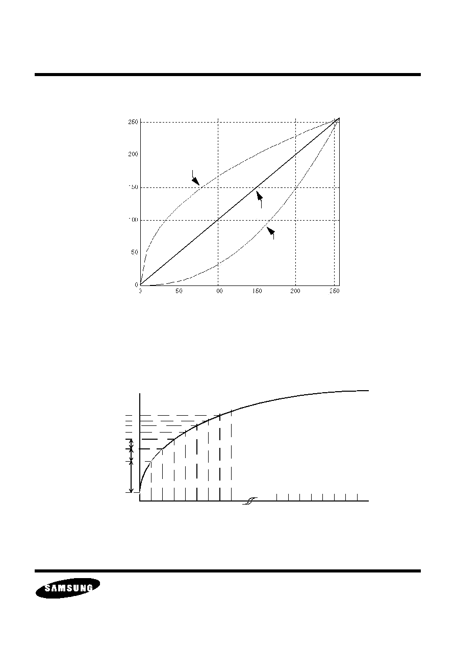
The S5D2650 programmable gamma tables allows the customer to apply many different type of corrections. These
corrections can be a standard 2.2 factor for NTSC or 2.8 for PAL. These factors can be applied in the RGB or YUV
domains.
A basic standard gamma equation of
when applied to the R, G, or B signals, generates the response shown as the upper curve below. It is the inverse of
the monitor response and thus compensates to produce a linear response.
J
J'
626
=
ELECTRONICS
S5D2650 Data Sheet
MULTIMEDIA VIDEO
PAGE 38 OF 95
7/18/03
Figure 32. RGB Gamma Correction
1.9.1. Programming the S5D2650
The previous response is easily programmed into the S5D2650 loading the 0, 8, 16, 24 etc. values into the
GAMMA0,1,2,3 locations. Thus every 8th value is stored. The S5D2650 will use linear interpolation to generate the
values between every 8th points. This is shown in the following figure.
Figure 33. Gamma LUT Programming
TV tube characteristic
Gamma correction
Effective output
0
8
16
24
32
40
48
56
64
192 200 208 216 224 232 240
248
Input
GAMMA0
GAMMA1
GAMMA2
GAMMA3
GAMMA4
GAMMA5
GAMMA6
GAMMA7
GAMMAD0
GAMMAD1
GAMMAD2
Output
ELECTRONICS
S5D2650 Data Sheet
MULTIMEDIA VIDEO
PAGE 39 OF 95
7/18/03
For ease of design, the difference between adjacent points must also be loaded. The complete data values for the
previous gamma factor of 1/2.2 is shown in the table below.
The flexibility of this architecture is shown in the following example. Here it is assumed that the S5D2650 is
operating in a YUV output mode but some form of Gamma correction is required. By converting the RGB gamma
correction function back to the YUV color space, the following function can be applied to the U and V signals for
improved color performance. This flexibility can be extended in software to produce many type of customer defined
transfer functions.
Table 10: RGB Gamma LUT Values
Offset
GAMMA
program at index Offset+40h
GAMMAD
program at index Offset+60h
0
0
53
1
53 20
2
73
14
3
87
12
4
99
11
5
110
10
6
120
8
7
128
8
8
136
8
9
144
7
A
151
7
B
158
6
C
164
6
D
170
6
E
176
5
F
181
6
10
187
5
11
192
5
12
197
5
13
202
5
14
207
4
15
211
5
16
216
4
17
220
5
18
225
4
19
229
4
1A
233
4
1B
237
4
1C
241
4
1D
245
4
1E
249
3
1F
252
4
ELECTRONICS
S5D2650 Data Sheet
MULTIMEDIA VIDEO
PAGE 40 OF 95
7/18/03
Figure 34. Gamma Correction for Cb and Cr
ELECTRONICS
S5D2650 Data Sheet
MULTIMEDIA VIDEO
PAGE 41 OF 95
7/18/03
1.10. DIGITAL VIDEO OUTPUT
The S5D2650 can output digital video data in various formats, which are tabulated in Table 11
.
All 8-bit output
Table 11: Digital Video Output Format
Clock
CK2
CK
OFMT
0
1
4
5
6
7
2, 3
Type
YCbCr
4:2:2
YCbCr 4:1:1
YCbCr
4:4:4
RGB
565
RGB
888
RGB
888
YCbCr 4:2:2
Pin
2N
+1
4N
+1
+2
+3
N
N
N
N
4N
+1
+2
+3
C0
Cb0
Cr0
Cb0
B0
B0
B3
C1
Cb1
Cr1
Cb1
B1
B1
B4
C2
Cb2
Cr2
Cb2
B2
B2
B5
C3
Cb3
Cr3
Cb3
B3
B3
B6
C4
Cb4
Cr4
Cr6
Cr4
Cr2
Cr0
Cb4
B4
B4
B7
C5
Cb5
Cr5
Cr7
Cr5
Cr3
Cr1
Cb5
G0
B5
G2
C6
Cb6
Cr6
Cb6
Cb4
Cb2
Cb0
Cb6
G1
B6
G3
C7
Cb7
Cr7
Cb7
Cb5
Cb3
Cb1
Cb7
G2
B7
G4
Y0
Y0
Y0
Y0
Y0
Y0
Y0
Y0
G3
G0
G5
Cb0
Y0
Cr0
Y0
Y1
Y1
Y1
Y1
Y1
Y1
Y1
Y1
G4
G1
G6
Cb1
Y1
Cr1
Y1
Y2
Y2
Y2
Y2
Y2
Y2
Y2
Y2
G5
G2
G7
Cb2
Y2
Cr2
Y2
Y3
Y3
Y3
Y3
Y3
Y3
Y3
Y3
R0
G3
R3
Cb3
Y3
Cr3
Y3
Y4
Y4
Y4
Y4
Y4
Y4
Y4
Y4
R1
G4
R4
Cb4
Y4
Cr4
Y4
Y5
Y5
Y5
Y5
Y5
Y5
Y5
Y5
R2
G5
R5
Cb5
Y5
Cr5
Y5
Y6
Y6
Y6
Y6
Y6
Y6
Y6
Y6
R3
G6
R6
Cb6
Y6
Cr6
Y6
Y7
Y7
Y7
Y7
Y7
Y7
Y7
Y7
R4
G7
R7
Cb7
Y7
Cr7
Y7
EXV0
Cr0
R0
B0
EXV1
Cr1
R1
B1
EXV2
Cr2
R2
B2
EXV3
Cr3
R3
G0
EXV4
Cr4
R4
G1
EXV5
Cr5
R5
R0
EXV6
Cr6
R6
R1
EXV7
Cr7
R7
R2

ELECTRONICS
S5D2650 Data Sheet
MULTIMEDIA VIDEO
PAGE 42 OF 95
7/18/03
formats use CK as pixel clock; the other formats use CK2 as pixel clock. The first pixel is always aligned to the
leading edge of the HAV signal.
1.10.1. Validation Code Insertion
S5D2650 inserts validation codes during inactive video (HAV is inactive), and invalid video (HAV is active but
EHAV is inactive) to assist in recognition of scaled data and VBI data. Table 12 lists the available codes, when they
are inserted, and related programming registers.
An example timing diagram for some of the programmable modes is shown in Figure 35. In this diagram, The field
rate is 60 Hz, A CCIR 601 sampling rate has been selected thus giving 720 active pixels. The horizontal scaling
ratio has been selected for an output of 718 out of 720 pixels.
Table 12: Invalid and Unused Code Insertion
Code
Description
INVALY
This user programmed code is inserted in the Y or G output stream in scaling operation when
HAV is active while EHAV is inactive. Insertion of this code is independent of the output
format. Related register is INVALY.
INVALU
This user programmed code is inserted in the U or B output stream in scaling operation when
HAV is active while EHAV is inactive. Insertion of this code is independent of the output
format. Related register is INVALU.
INVALV
This user programmed code is inserted in the V or R output stream in scaling operation when
HAV is active while EHAV is inactive. Insertion of this code is independent of the output
format. Related register is INVALV.
UNUSEY
This user programmed code is inserted in the Y or G output stream when HAV is inactive and
no other reference code is inserted. Insertion of this code is independent of the output format.
Related register is UNUSEY.
UNUSEU
This user programmed code is inserted in the U or B output stream when HAV is inactive and
no other reference code is inserted. Insertion of this code is independent of the output format.
Related register is UNUSEU.
UNUSEV
This user programmed code is inserted in the V or R output stream when HAV is inactive and
no other reference code is inserted. Insertion of this code is independent of the output format.
Related register is UNUSEV.
ELECTRONICS
S5D2650 Data Sheet
MULTIMEDIA VIDEO
PAGE 43 OF 95
7/18/03
Figure 35. Horizontal Data Timing for Various Output Modes
1.10.2. 656 Op Codes
The S5D2650 supports timing synchronization through embedded (656) timing reference codes in the output video
data stream. This mode is available for output format 3 ( OFMT[3:0] = 3). The 656 Op Codes follow the CCIR 656
standard. An optional set of 656 Op Codes can be enabled to identify VBI data using the TASKB bit.
The (A,B,C,D) inserted codes for 656 output modes are explained below. Locations in the data stream are shown
in Figure 35. The D' data is substituted for the standard codes shown in column D if TASKB bit is set and the
current line is processing VBI data (sliced or raw ADC data format).
U
U
U
U
U
U
U
I
U
I
U
I
U
I
U
0
U
1
U
2
U
3
Y
0
U
714
Y
715
U
U
U
U
Y
U
Y
U
Y
U
Y
I
Y
I
Y
I
Y
I
Y
0
Y
1
Y
2
Y
3
Y
0
Y
T714
Y
Y715
Y
U
Y
U
V
U
V
U
V
U
V
I
V
I
V
I
V
I
V
0
V
1
V
2
V
3
V
0-
V
714
V
715
V
U
V
U
V
U
U
U
V
U
U
I
V
I
U
I
V
I
U
0
V
0
U
2
V
2
Y
0
U
714
V
714
U
U
V
U
EHAV
CK
CK2
HAV
Y
0
Y
U
Y
U
V
U
Y
U
U
U
Y
U
Y
U
V
U
Y
I
Y
I
Y
I
Y
U
U
I
Y
I
V
I
Y
I
U
I
Y
I
V
I
Y
I
U
0
Y
0
V
0
Y
1
U
2
Y
2
V
2
Y
3
Y
0
Y
0
U
x
Y
x
V
x
Y
x
U
U
Y
U
V
U
Y
I
Y
0
Y
1
Y
2
Y
3
Y
0
Y
714
Y
715
Y
U
Y
U
Legend
Luma Data with pixel number
U
0
Chroma (Cb) Data with pixel number
V
0
Chroma (Cr) Data with pixel number
Y
I
Programmable INVALY data (index 0x32)
U
I
Programmable INVALU data (index 0x33)
V
I
Programmable INVALV data (index 0x34)
Y
U
Programmable UNUSEY data (index 0x35)
U
U
Programmable UNUSEU data (index 0x36)
V
U
Programmable UNUSEV data (index 0x37)
OFMT=0 (16 bits @ 13.5 Mhz 4:2:2 - 601)
Invalid data (During
Active Video but Scaling
Has made picture smaller
and right justified)
Unused Data
OFMT=2 (8 bits @ 27 Mhz 656 data no SAV EAV)
Unused Data
If Horizontal Scaling is
disabled, EHAV will be the same
as HAV and there will be no
Invalid data. For this Example,
the last Data would be
Y
719
OFMT= 3
A
B
C
D
SAV -- see Table
12 for details
A
B
C
D
EAV -- see table for details
Same Format as OFMT=2
OFMT=4 (24 bits @ 13.5 Mhz YUV 4:4:4)
Y[7:0]
C[7:0]
Y[7:0]
Y[7:0]
C[7:0]
EXV[7:0]
ELECTRONICS
S5D2650 Data Sheet
MULTIMEDIA VIDEO
PAGE 44 OF 95
7/18/03
Figure 36. Vertical Timing for 60 Hz Video
Fields
2,4
ODD
ODD
263
264
265
266
267
268
269
270
1
2
3
4
5
6
7
8
9
10
20
21
271
272
273
525
284
283
Fields
1,3
60 Hz EVEN FIELD
60 Hz ODD FIELD
VS
VS
VALIGN=0
VS
VALIGN=0
ODD
0
0
0
0
0
0
0
-
1
1
0
11
VBIL[N]
656 SAV EAV Codes for VSE=0, VALIGN=1
Digital
Output
VALIGN=0
ODD
VALIGN=1
VALIGN=0
VS
VALIGN=1
VBIL[N]
Y[0..7]
VALIGN=1
F1 EC F1 EC F1EC B6AB B6AB B6AB B6AB B6AB B6AB 9D80
9D80 9D80
9D80
VSE=1
VSE=0
VSE=0
VSE=1
VSE=1
VSE=0
VSE=1
VSE=0
VSE=0
VSE=1
VSE=0
VSE=1
Y[0..7]
B6AB B6AB F1 EC F1EC F1EC F1 EC F1 EC F1 EC F1 EC F1C7 DAC7 DAC7 DAC7
VSE=1
VSE=0
VSE=1
VSE=0
VSE=0
VSE=1
VSE=1
VSE=0
656 SAV EAV Codes for VSE=0, VALIGN=1
VALIGN=1
DAC7
9D80
1
2
3
4
5
6
7
8
9
10
20
21
Input
Analog
22
Digital
output
264
265
266
267
268
269
270
271
272
273
284
283
Analog
Input
285
SAV
EAV
SAV
EAV
TASK B VIP 656 SAV EAV Codes for VSE=0, VALIGN=1, VBIL12-VBIL1=1, TASKB=1
Y[0..7]
F1EC F1EC F1 EC B6AB B6AB B6AB B6AB B6AB B624 13 0E 13 0E 13 0E
13 80
DAC7
15
23
24
22
23
14
13
12
0
0
13 80 9D80 9D80
9D80
9D80 9D80
524
525
285
286
286
287
262
263
0
0
0
0
0
0
0
-
1
1
0
11
15
14
13
12
0
0
DAC7 DAC7 DAC7
9D80
DAC7
DAC7
B6AB B6AB F1 EC F1 EC F1 EC F1EC F1EC F1 EC F1 62 7F 62
7F62
7F62
7F62
9D80
7FC7 DAC7 DAC7
9D80
Y[0..7]
TASK B VIP 656 SAV EAV Codes for VSE=0, VALIGN=1, VBIL12-VBIL1=1, TASKB=1
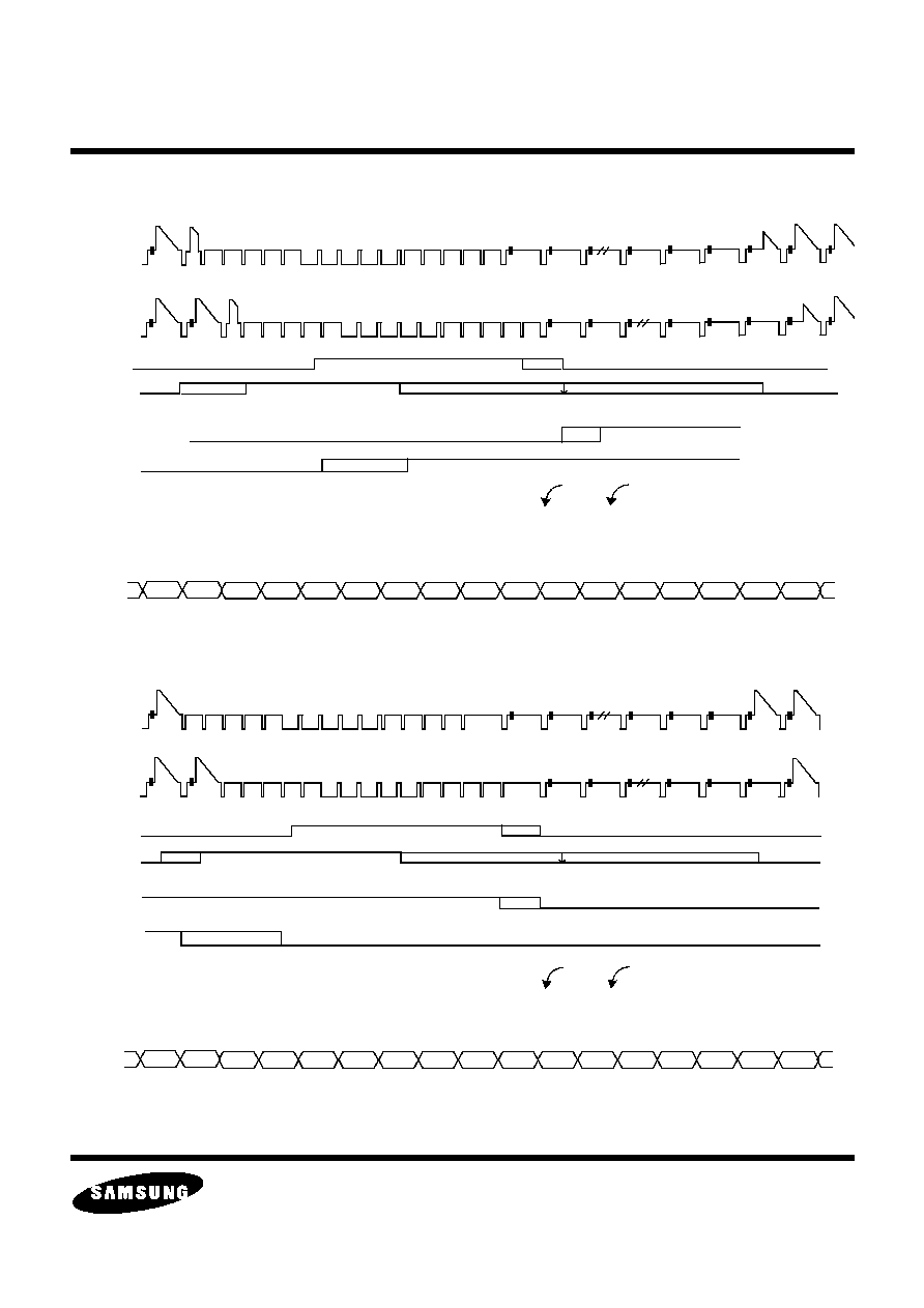
ELECTRONICS
S5D2650 Data Sheet
MULTIMEDIA VIDEO
PAGE 45 OF 95
7/18/03
Figure 37. Vertical Timing For 50 Hz Video
VS
ODD
623
624
625
1
2
3
4
5
6
7
622
Fields
1,3
50 Hz ODD FIELD
VS
VALIGN=0
ODD
Digital
Output
VS
VALIGN=1
ODD
VALIGN=1
0
0
0
0
0
0
0
-
1
1
0
14
VBIL[N]
ODD
VALIGN=1
VS
VALIGN=1
VSE=0
VSE=1
VSE=1
VSE=0
VSE=1
VSE=1
VSE=0
VALIGN=0
VSE=1
VSE=0
Y[0..7]
DAC7 F1EC F1EC
B6AB B6AB B6AB B6AB B6AB B6AB B6AB B6AB B6
656 SAV EAV Codes for VSE=0, VALIGN=1
Fields
2,4
310
311
312
313
314
315
316
317
318
319
320
50 Hz EVEN FIELD
VSE=0
VSE=1
VALIGN=0
VSE=1
VSE=1
VSE=0
VSE=0
VSE=1
VALIGN=0
VSE=1
VSE=-0
20
21
22
23
24
621
623
624
625
1
2
3
4
5
6
7
622
20
21
22
23
24
Analog
Input
25
15
15
0
0
0
AB 9D 80 9D 80 9D
DAC7
DAC7
VSE=0, ALT656=0
VSE=0, ALT656=1
SAV
EAV
TASK B VIP 656 SAV EAV Codes for VSE=0, VALIGN=1, ALT656=1, VBIL15-VBIL1=1, TASKB=1
Y[0..7]
DAC7 DAC7 DAC7 F1EC F1EC B6AB B6AB B6AB B6AB B624
13 0E 13 0E 13 0E 130E 13 80 9D 80
DAC7
DAC7
0
0
0
0
0
0
0
-
1
1
0
14
VBIL[N]
15
15
0
0
0
Y[0..7]
B6AB B6AB F1 EC F1EC F1EC F1EC F1EC F1EC F1EC F1EC F1EC F1EC F1EC F1
656 SAV EAV Codes for VSE=0, VALIGN=1
EC DAC7 DA C7 D
9D80
9D80
SAV
EAV
TASK B VIP 656 SAV EAV Codes for VSE=0, VALIGN=1, ALT656=1, VBIL15-VBIL1=1, TASKB=1
Y[0..7]
310
311
312
313
314
315
316
317
318
319
320
Digital
Output
Analog
Input
333
334
335
336
333
334
335
336
337
VSE=0, ALT656=0
VSE=0, ALT656=1
B6AB B6AB F1EC F1EC F1EC F1EC F1EC F1EC F162 54 49 54 49 54 49
54 49 54 49 54 C7 DA C7
9D80
9D80
B6AB B6AB
ELECTRONICS
S5D2650 Data Sheet
MULTIMEDIA VIDEO
PAGE 46 OF 95
7/18/03
1.10.3. 656 Op Code Vertical Transitions
The vertical transition locations of the various 656 Op Codes are shown in Figure 36 and Figure 37. Note that for
proper transition locations of the SAV and EAV Op Codes VSE=0 and VALIGN=1.
1.11. HOST INTERFACE
The S5D2650 supports the IIC serial interface for programming the chip registers.
1.11.1. IIC Interface
The two wire interface consists of the SCLK and SDAT signals. Data can be written to or read from the S5D2650.
For both read and write, each byte is transferred MSB first, and the data bit is valid when the SCLK is high.
To write to the slave device, the host initiates a transfer cycle with a START signal. The START signal is HIGH to
LOW transition on the SDAT while the SCLK is high. The host then sends a byte consisting of the 7-bit slave device
ID and a 0 in the R/W bit. The arrangement for the slave device ID and the R/W bit is depicted in Figure 38. AEX1
and AEX0 are configuration pins used to configure the S5D2650 to use one of the four addresses. Up to four
S5D2650's can be used in one system each with a unique address.
Figure 38. IIC Slave Device ID and R/W Byte
Table 13: 656 and TASKB 656 Op Codes
Condition
SAV / EAV Output Sequence --
Reference Output timing
pictures
656 FVH values
(low active)
Field
Vertical
Horizontal
A
B
C
D
(active)
D'
(vbi)
F
V
H
Field 2
Vertical Blank
End Active Video
FFh
00h
00h
F1h
7Fh
1
1
1
Field 2
Vertical Blank
Start Active Video
FFh
00h
00h
ECh
62h
1
1
0
Field 2
Vertical Active
End Active Video
FFh
00h
00h
DAh
54h
1
0
1
Field 2
Vertical Active
Start Active Video
FFh
00h
00h
C7h
49h
1
0
0
Field 1
Vertical Blank
End Active Video
FFh
00h
00h
B6h
38h
0
1
1
Field 1
Vertical Blank
Start Active Video
FFh
00h
00h
ABh
24h
0
1
0
Field 1
Vertical Active
End Active Video
FFh
00h
00h
9Dh
13h
0
0
1
Field 1
Vertical Active
Start Active Video
FFh
00h
00h
80h
0Eh
0
0
0
1
1
0
1
1
AEX1
AEX0
R/W
msb
lsb
slave device ID
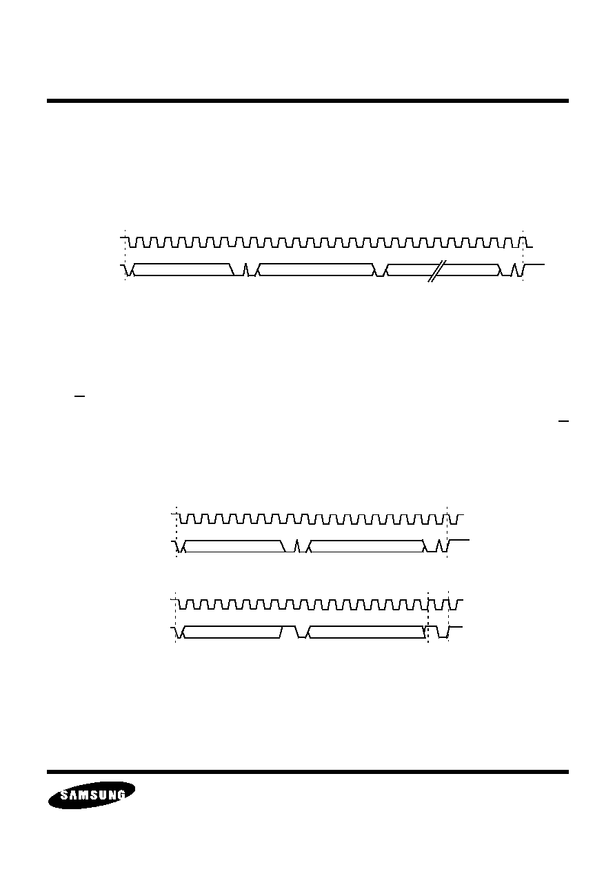
ELECTRONICS
S5D2650 Data Sheet
MULTIMEDIA VIDEO
PAGE 47 OF 95
7/18/03
The second byte the host sends is the base register index. The host then sends the data. The S5D2650
increments the index automatically after each byte of data is sent. Therefore, the host can write multiple bytes to
the slave if they are in sequential order. The host completes the transfer cycle with a STOP signal which is a LOW
to HIGH transition when the SCLK is high.
Each byte transfer consists of 9 clocks. When writing to the S5D2650, an acknowledge signal is asserted by the
salve device during the 9th clock.
Figure 39. IIC Data Write
A read cycle takes two START-STOP phases. The first phase is a write to the index register. The second phase is
the read from the data register.
The host initiates the first phase by sending the START signal. It then sends the slave device ID along with a 0 in
the R/W position. The index is then sent followed by the STOP signal.
The second phase also starts with the START signal. It then sends the slave device ID but with a 1 in the R/W
position to indicate data is to be read from the slave device. The host uses the SCLK to shift data out from the
S5D2650. A typical second phase in a read transaction is depicted in Figure 40. Auto index increment is supported
in Read mode.
Figure 40. IIC Data Read
SCLK
SDAT
device ID
index
data
data
START
STOP
ACK
ACK
ACK
SCLK
SDAT
device ID
index
START
STOP
ACK
ACK
SCLK
SDAT
device ID
data
START
STOP
NACK
ELECTRONICS
S5D2650 Data Sheet
MULTIMEDIA VIDEO
PAGE 48 OF 95
7/18/03
2. CONTROL REGISTER DESCRIPTION
This section contains information concerning the programmable control registers. Table 14 provides the default
power up values for each index, and a bit map for each register. The following pages describe each register in
detail and the possible programing values (an * indicates the power-on default). Gamma correction registers are
write only. When the index register points to any of the Gamma correction register, the Gamma look-up table is put
into a program mode. Normal operation resumes when the index is outside the range from 0x40 to 0xFF.
Table 14: Register Summary
Index Mnemonic Default
Bit Map
7
6
5
4
3
2
1
0
0x00
STAT
RO
CHIPID
VBIFLG
NOVID
FFRDET
PALDET
CDET
HLOCK
CLOCK
0x01
CMDA
2C
POWDN
VSE
HFSEL[1:0]
XT24
PIXSEL
MNFMT
IFMT
0x02
CMDB
20
AGCGN
VALIGN
AGCOVF
AGCFRZ COMP_PH
INSEL[2:0]
0x03
CMDC
40
VMEN
TSTGE1
0
TSTGPK
TSTGPH
TSTGFR[1:0]
TSTGEN
0x04
CMDD
40
EAV
CADC_PD
CKDIR
INPSL[1:0]
SYNDIR
PROG
GPPORT
0x05
HAVB
00
HAVB[7:0]
0x06
HAVE
00
HAVE[7:0]
0x07
HS1B
14
HS1B[8:1]
0x08
HS1E
40
HS1E[8:1]
0x09
HS2B
00
HS2B[8:1]
0x0A
HS2E
00
HS2E[8:1]
0x0B
AGC
80
AGC[7:0]
0x0C
HXTRA
00
HAVB[10:8]
HAVE[10:8]
HS1BE0
HS2BE0
0x0D
CDEM
00
OUTHIZ
FSEC
TBC_ON
CIFCMP[1:0]
0
0
0
0x0E
PORTAB
00
DIRB
DATAB[2:0]
DIRA
DATAA[2:0]
0x0F
LUMA
02
0
UNIT
RGBH
PED
HYBWR
CTRAP
HYPK[1:0]
0x10
CON
00
CONT[7:0]
0x11
BRT
00
BRT[7:0]
0x12
CHROMA
08
ACCFRZ
PALM
PALN
CBW
CORE[1:0]
CKILL[1:0]
0x13
CHROMB
C0
CDLY[3:0]
SCHCMP[3:0]
0x14
DEMOD
00
FSCDET
SECDET
CDMLPF
CTRACK
MNFSC[1:0]
MNSECAM[1:0]
0x15
SAT
00
SAT[7:0]
0x16
HUE
00
HUE[7:0]
0x17
VERTIA
00
MNYCMB
YCMBCO[2:0]
VRT2X
VCTRL[2:0]
0x18
VERTIB
14
HYLPF[2:0]
HYBWI
HYDEC
VSCLEN[1:0]
0
0x19
VERTIC
0B
MNCCMB
CCMBCO[2:0]
ACMBEN
VYBW
EVAVEV
EVAVOD
0x1A
HSCLL
01
HSCL[6:0]
CMBMOD
0x1B
HSCLH
00
HSCL[14:7]
0x1C
VSCLL
FC
VSCL[5:0]
ACMBCO ACMBRE
0x1D
VSCLH
FF
VSCL[13:6]
0x1E
OFMTA
00
GAMEN[1:0]
OENC[1:0]
OFMT[3:0]
0x1F
OFMTB
00
VSVAV
EVAND[1:0]
EVHS1
EVHAV
EVEHAV
EVAVG
EVANDL
ELECTRONICS
S5D2650 Data Sheet
MULTIMEDIA VIDEO
PAGE 49 OF 95
7/18/03
0x20
VBICTL
00
VBCVBS
VYFMT[1:0]
VBINSRT
ODDEN
EVENEN
ODDOS[1:0]
0x21
CCDAT1
RO
b0
b1
b2
b3
b4
b5
b6
P1
0x22
CCDAT2
RO
b0
b1
b2
b3
b4
b5
b6
P2
0x23
VBIL30
00
VBIL3
VBIL2
VBIL1
VBIL0
0x24
VBIL74
00
VBIL7
VBIL6
VBIL5
VBIL4
0x25
VBIL118
00
VBIL11
VBIL10
VBIL9
VBIL8
0x26
VBIL1512
00
VBIL15
VBIL14
VBIL13
VBIL12
0x27
TTFRAM
00
TTFRAM[7:0]
0x28
TESTA
00
0
0
0
0
0
0
0
0
0x29
UVOFFH
00
TSTCLC
TSTCGN
0
TSTCFR
UOFFST[5:4]
VOFFST[5:4]
0x2A
UVOFFL
33
UOFFST[3:0]
VOFFST[3:0]
0x2B
UGAIN
00
UGAIN[7:0]
0x2C
VGAIN
00
VGAIN[7:0]
0x2D
VAVB
23
VAVB[6:1]
VAVOD0
VAVEV0
0x2E
VAVE
82
VAVE[8:1]
0x2F
CTRACK
00
0
0
DMCTL[1:0]
CGTC[1:0]
CFTC[1:0]
0x30
POLCTL
00
EVAVPL
VSPL
ODDPL
HAVPL
EHAVPL
HS2PL
VAVPL
HS1PL
0x31
REFCOD
00
YCRANG
0
0
0
0
0
0
0
0x32
INVALY
10
INVALY[7:0]
0x33
INVALU
80
INVALU[7:0]
0x34
INVALV
80
INVALV[7:0]
0x35
UNUSEY
10
UNUSEY[7:0]
0x36
UNUSEU
80
UNUSEU[7:0]
0x37
UNUSEV
80
UNUSEV[7:0]
0x38
EXCTRL
04
PERMIN
ENINCST
SLEV[1:0]
OFFST_CONT[1:0]
0
CLEVEL
0x39
TRACKA
00
STCTRL
MAC_DET
VCR_DET
VCR_LEV[1:0]
ATCTRAP VCTRAP
AGCLSB
0x3A
VBICTLB
00
VBISWAP
TT_SYS[1:0]
VBIMID
NEW_CC CC_OVFL YOFFENB COFFENB
0x3B
TRACKB
00
ALT656
VBI_PH
VBI_FR
PH_CTRL VNOISCT
AGC_LPG[1:0]
AGC_LKG
0x3C
RTC
00
RTC_DTO RTC_PID SEC_POL
TDMOD
VCO_BIAS[1:0]
PUMP_BIAS[1:0]
0x3D
CMDE
2C
ODFST
VSALG
HCORE[1:0]
CHIPREVID
0x3E
VSDEL
00
TR_MS
NOVIDC
VSDEC[5:0]
0x3F
CMDF
00
CTRAPFSC
VIPMODE
EVAVY
UVDLEN
UVDLSL
REGUD
TASKB
CBWI
0x40-5F
GAMMA
-
GAMMA0[7:0] - GAMMA31[7:0]
0x60-7F
GAMMAD
-
-
-
GAMMAD0[5:0] - GAMMAD31[5:0]
0xC0-DF
GAMUV
-
GAMUV0[7:0] - GAMUV31[7:0]
0xE0-FF
GAMUVD
-
-
-
GAMUVD0[5:0] - GAMUVD31[5:0]
Table 14: Register Summary
Index Mnemonic Default
Bit Map
7
6
5
4
3
2
1
0

ELECTRONICS
S5D2650 Data Sheet
MULTIMEDIA VIDEO
PAGE 50 OF 95
7/18/03
Read Only Status Bits
Index
Mnemonic
bit 7
bit 6
bit 5
bit 4
bit 3
bit 2
bit 1
bit 0
00h
STAT
CHIPID
VBIFLG
NOVID
FFRDET
PALDET
CDET
HLOCK
CLOCK
CLOCK
Status for color lock.
0
Not locked.
1
Color lock achieved.
HLOCK
Status for current line tracking mode.
0
Chip is in initial tracking mode.
1
Chip is in steady state tracking mode.
CDET
Status for detection of color.
0
No color signal is detected.
1
Color signal is detected.
PALDET
Status for current detected color format. Information contained in this bit is valid only if
CLOCK is 1.
0
NTSC color format.
1
PAL color format.
FFRDET
Status for current detected field frequency.
0
50 Hz field frequency, i.e. N,B,G,H,I,D,K,K1,L system.
1
60 Hz field frequency, i.e. M system.
NOVID
Video detect flag. This bit should not be used for detecting the presence of a TV channel
from the output of a TV tuner.
0
Sync has been detected for the last 32 lines.
1
No sync has been detected.
VBIFLG
Vertical blanking interval flag.
0
Video is in active region.
1
Video is in vertical blanking region.
CHIPID
Chip version ID. Please refer to the CHIPREVID bits for additional information
0
KS0127B.
1
S5D2650.

ELECTRONICS
S5D2650 Data Sheet
MULTIMEDIA VIDEO
PAGE 51 OF 95
7/18/03
Control Register A
Index
Mnemonic
bit 7
bit 6
bit 5
bit 4
bit 3
bit 2
bit 1
bit 0
01h
CMDA
POWDN
VSE
HFSEL[1:0]
XT24
PIXSEL
MNFMT
IFMT
IFMT
Manual video input standard select. Standard selection can be controlled automatically if
MNFMT=0.
0
Chip is forced to assume input is 50 Hz.*
1
Chip is forced to assume input is 60 Hz.
MNFMT
Manual input format control override. When this bit is 1 the IFMT bit is enabled.
0
The chip determines the input video standard based on the detected field rate:*
NTSC if 60 Hz.
PAL/SECAM if 50 Hz.
1
Input video standard is selected with the IFMT bit.
PIXSEL
Select pixel sampling rate.
0
Output data is at square pixel rate.
1
Output data is at CCIR 601 rate.*
XT24
Select the external clock reference frequency.
0
External clock is 26.8 MHz.
1
External clock is 24.576 MHz.*
HFSEL[1:0]
Horizontal tracking loop frequency select.
0
Force loop to very fast.
1
Force loop to fast.
2
Force loop to VCR time constant.*
3
Force loop to TV time constant.
VSE
Change the vertical end location of the VS.
0
Line 10/10.5.*
1
Line 9/9.5.
POWDN
Power down mode.
0
Normal operation.*
1
All chip functions except microprocessor interface and CK/CK2 generation are
disabled. The output of the CK/CK2 pins retains the most recent frequency when
the power down mode is enabled.

ELECTRONICS
S5D2650 Data Sheet
MULTIMEDIA VIDEO
PAGE 52 OF 95
7/18/03
Control Register B
Index
Mnemonic
bit 7
bit 6
bit 5
bit 4
bit 3
bit 2
bit 1
bit 0
02h
CMDB
AGCGN
VALIGN
AGCOVF
AGCFRZ COMP_PH
INSEL[2:0]
INSEL[2:0]
Analog input channel select.
0
AY0 is composite input.*
1
AY1 is composite input.
2
ACR0 is composite input.
3
ACR1 is composite input.
4
AY0 is Luminance input, ACB0 is chrominance input.
5
AY1 is Luminance input, ACB1 is chrominance input.
6
AY0 is luminance input, ACB0 is Cb input, ACR0 is Cr input.
7
AY1 is luminance input, ACB1 is Cb input, ACR1 is Cr input.
COMP_PH
Cb & Cr phase inversion in case of Component input
0
Normal operation *
1
Phase inversion
AGCFRZ
Freeze the analog AGC for the Y and C paths at their current values.
0
AGC is running. Reading AGC register returns the current AGC gain.*
1
AGC is frozen. Gain can be changed or read with AGC register.
AGCOVF
AGC gain control mode.
0
AGC gain tracks to sync tip and back porch delta.
1
If ADC overflows, AGC gain will be reduced (this has higher priority over normal
sync tip - back porch tracking).*
VALIGN
VS edge alignment control.
0
VS leading edge occurs during serration pulses (typically within the first serration
pulse). VS trailing edge is aligned to half line or beginning of the line depending on
the field.*
1
VS leading edge is aligned to half line or beginning of the line depending on the
field. VS trailing edge is always aligned to beginning of the line.
AGCGN
AGC gain calculation.
0
Normal mode. AGC gain calculation is based on sync tip to back porch difference
equal to 68 ADC code.*
1
AGC gain calculation is base on sync tip to back porch difference equal to 54 ADC
code. This will reduce the AGC gain by a factor of 1/1.25 compare to normal mode.
When used in conjunction with PED and RGBH, this effectively increases the input
dynamic range.

ELECTRONICS
S5D2650 Data Sheet
MULTIMEDIA VIDEO
PAGE 53 OF 95
7/18/03
Control register C
Index
Mnemonic
bit 7
bit 6
bit 5
bit 4
bit 3
bit 2
bit 1
bit 0
03h
CMDC
VMEN
TSTGE1
0
TSTGPK
TSTGPH
TSTGFR[1:0]
TSTGEN
TSTGEN
Enable manual control of horizontal phase and frequency tracking.
0
Auto phase and frequency tracking.*
1
Enable manual control of horizontal phase and frequency with TSTGFR[1:0] and
TSTGPH.
TSTGFR[1:0]
When TSTGEN == 1, these two bits control the horizontal frequency tracking.
00
Stop frequency tracking and freeze the frequency at the current value.*
01
Horizontal frequency tracks the input.
1X
Horizontal frequency tracking ignores video input and runs at nominal value based
on the field rate and output pixel rate selected by IFMT and PIXEL bits.
TSTGPH
When TSTGEN == 1, this bit controls the horizontal phase tracking.
0
No phase tracking.*
1
Horizontal phase tracks the input video or HS1 input if in slave mode.
TSTGPK
If TSTGE1 == 1, this bit controls AGC.
0
AGC clamps to back porch and gain is set based on sync tip-back porch difference.*
1
AGC clamps to sync tip and gain is set based on peak-valley difference.
TSTGE1
Enables the function of TSTGPK.
0
Disables TSTGPK.*
1
Enables TSTGPK.
VMEN
Vertical master mode.
0
Normal vertical sync operation.*
1
Vertical sync ignores input and free runs at 50 Hz or 60 Hz. This mode can be used
to generate video timing for a slave device.

ELECTRONICS
S5D2650 Data Sheet
MULTIMEDIA VIDEO
PAGE 54 OF 95
7/18/03
Control Register D
Index
Mnemonic
bit 7
bit 6
bit 5
bit 4
bit 3
bit 2
bit 1
bit 0
04h
CMDD
EAV
CADC_PD
CKDIR
INPSL[1:0]
SYNDIR
PROG
GPPORT
GPPORT
General purpose port. This register is useful only if DATAA[2:0] == 7. If DIRA == 0, this bit is
read only and reflects the logic state at PORTA pin. If DIRA == 1, any value written to this bit will
appear at PORTA pin.
PROG
Progressive YPbPr Input Mode, ADC sampling clock = 54 MHz
0
Interlaced YPbPr Input Mode.(720x480i)
1
Progressive YPbPr Input Mode.(720x480p)
SYNDIR
HS1 and VS pin direction control.
0
HS1 and VS are output.*
1
HS1 and VS are input.
INPSL[1:0]
Video input and clock source select.
0
Video source is analog and connected to the chip's analog input. Clock is internally
generated.*
1
Video source is 8-bit digital CbYCr and connected to EXV0 through EXV7 pins.
3
Video source is 8-bit digitized CVBS and connected to EXV0 through EXV7 pins.
CKDIR
Clock select.
0
Clock is from internal clock generator. A reference clock at XTALI pin is required.*
1
Clock is from CK pin. When this is selected, the CK pin automatically becomes an
input.
CADC_PD
C-ADC's Power down mode.
0
All ADC's Power On.
1
C-ADC's Power Down, in case of CVBS input modes*.
EAV
In 8-bit digital CbYCr input mode, this bit selects the sync source.
0
Horizontal and vertical syncs are from HS1 and VS pins, respectively.*
1
Syncs are embedded in the 8-bit digital data stream (CCIR 656 compatible).
ELECTRONICS
S5D2650 Data Sheet
MULTIMEDIA VIDEO
PAGE 55 OF 95
7/18/03
HAV Start Control
Index
Mnemonic
bit 7
bit 6
bit 5
bit 4
bit 3
bit 2
bit 1
bit 0
05h
HAVB
HAVB[7:0]
0Ch
HXTRA
HAVB[10:8]
HAVE[10:8]
HS1BE0
HS2BE0
HAVB[10:0]
This 11-bit register is used to define the start location of the HAV signal relative to the sync tip
(for CVBS input, this is the composite video sync tip. For 8-bit CbYCr input, this is the leading
edge of the HS1 or EAV). The content of this register is a 2's complement number which is
used as an offset to the default. The resolution for this register is 1 CK clock.
HAV End Control
Index
Mnemonic
bit 7
bit 6
bit 5
bit 4
bit 3
bit 2
bit 1
bit 0
06h
HAVE
HAVE[7:0]
0Ch
HXTRA
HAVB[10:8]
HAVE[10:8]
HS1BE0
HS2BE0
HAVE[10:0]
This 11-bit register is used to define the end location of the HAV signal relative to the sync tip.
The content of this register is a 2's complement number which is used as an offset to the
default The resolution for this register is 1 CK clock.
HS1 Start Control
Index
Mnemonic
bit 7
bit 6
bit 5
bit 4
bit 3
bit 2
bit 1
bit 0
07h
HS1B
HS1B[8:1]
0Ch
HXTRA
HAVB[10:8]
HAVE[10:8]
HS1BE0
HS2BE0
HS1B[8:1] -
HS1BE0
If HS1 is programmed as an output, this 9-bit register defines the start location of the HS1
signal. The content of this register is a 2's complement number which is used as an offset to the
default. The resolution for this register is 1 CK clock.
ELECTRONICS
S5D2650 Data Sheet
MULTIMEDIA VIDEO
PAGE 56 OF 95
7/18/03
HS1 End Control
Index
Mnemonic
bit 7
bit 6
bit 5
bit 4
bit 3
bit 2
bit 1
bit 0
08h
HS1E
HS1E[8:1]
0Ch
HXTRA
HAVB[10:8]
HAVE[10:8]
HS1BE0
HS2BE0
HS1E[8:1] -
HS1BE0
If HS1 is programmed as an output, this 9-bit register defines the end location of the HS1
signal. The content of this register is a 2's complement number which is used as an offset to the
default. The resolution for this register is 1 CK clock.
HS2 Start Control
Index
Mnemonic
bit 7
bit 6
bit 5
bit 4
bit 3
bit 2
bit 1
bit 0
09h
HS2B
HS2B[8:1]
0Ch
HXTRA
HAVB[10:8]
HAVE[10:8]
HS1BE0
HS2BE0
HS2B[8:1] -
HS2BE0
This 9-bit register defines the start location of the HS2 signal. The content of this register is a
2's complement number which is used as an offset to the default HS2B location. The resolution
for this register is 1 CK clock.
HS2 End Control
Index
Mnemonic
bit 7
bit 6
bit 5
bit 4
bit 3
bit 2
bit 1
bit 0
0Ah
HS2E
HS2E[8:1]
0Ch
HXTRA
HAVB[10:8]
HAVE[10:8]
HS1BE0
HS2BE0
HS2E[8:1] -
HS2BE0
This 9-bit register defines the end location of the HS2 signal. The content of this register is a 2's
complement number which is used as an offset to the default HS2E location. The resolution for
this register is 1 CK clock.
ELECTRONICS
S5D2650 Data Sheet
MULTIMEDIA VIDEO
PAGE 57 OF 95
7/18/03
AGC Control
Index
Mnemonic
bit 7
bit 6
bit 5
bit 4
bit 3
bit 2
bit 1
bit 0
0x0B
AGC
AGC[7:0]
AGC[7:0]
This register is used to manually set AGC when AGCFRZ is set to "1". The content in the
register is unsigned.
Chroma Demodulation Control
Index
Mnemonic
bit 7
bit 6
bit 5
bit 4
bit 3
bit 2
bit 1
bit 0
0Dh
CDEM
OUTHIZ
FSEC
TBC_ON
CIFCMP[1:0]
0
0
0
CIFCMP[1:0]
IF compensation for the chroma path.
0
No compensation.*
1
Upper chroma side band is 1 dB higher than lower side band.
2
Upper chroma side band is 3 dB higher than lower side band.
3
Upper chroma side band is 6 dB higher than lower side band.
TBC_ON
Time based correction Test Mode
0
Normal operation*
1
TBC Test mode.
FSEC
Chroma frequency demodulation filter select for SECAM video.
0
Select SECAM chroma frequency demodulation filter if SECAM video is detected.*
1
Always use SECAM chroma frequency demodulation filter.
OUTHIZ
This is the software output three-state control bit. If this bit is set to a "1", or the OEN pin is at a
logic LOW level, output pins can be selectively put in the high impedance state using the
additional software control bits OENC[1:0].
0
This is default setting.*
1
This will enable the output pins to be three-stated regardless the state of the OEN
pin.

ELECTRONICS
S5D2650 Data Sheet
MULTIMEDIA VIDEO
PAGE 58 OF 95
7/18/03
Port A and B Control
Index
Mnemonic
bit 7
bit 6
bit 5
bit 4
bit 3
bit 2
bit 1
bit 0
0Eh
PORTAB
DIRB
DATAB[2:0]
DIRA
DATAA[2:0]
DATAA[2:0]
Port A data select. For internal gate signal locations.
0
Port A is disconnected from the internal signal path.*
1
Port A is connected to the BPG (back porch gate) signal.
2
Port A is connected to the SYG (sync tip gate) signal.
3
Port A is connected to the CBG (color burst gate) signal.
4
Port A is connected to the CBGW (color burst gate wide) signal. The CBGW is high
for the entire color burst period.
5
Port A is connected to the SLICE (mid way of the sync tip) signal.
6
Port A is connected to the VBI (vertical blanking interval) signal.
7
Port A is connect to the GPPORT bit.
DIRA
Port A direction control.
0
Port A is configured as input. The input is connected directly to the signal path
selected by DATAA[2:0]. The internally generated gate signal is disconnected from
the signal path.*
1
Port A is an output and is driven by the internally generated signal as selected by
DATAA[2:0].
DATAB[2:0]
Port B data select. For internal gate signal locations.
0
Port B is disconnected from the internal signal path.*
1
Port B is disconnected.
2
Port B is connected to the FH2 (twice per line pulses) signal.
3
Port B is connected to the FS_PULSE (falling edge of the sync tip) signal.
4
Port B is connected to the VBI_CVBS (VBI raw ADC) signal. This signal is high for
those lines that output data directly from the ADC (not YUV or RGB data).
5
Port B is connected to the VBI_PROC (VBI sliced) signal. This signal is high for
those video lines that output sliced VBI data.
6
Port B is connected to the COFF signal.
7
Port B is disconnected.
DIRB
Port B direction control.
0
Port B is configured as input. The input is connected directly to the signal path
selected by DATAB[2:0]. The internally generated gate signal is disconnected from
the signal path.*
1
Port B is an output and is driven by the internally generated signal as selected by
DATAB[2:0].

ELECTRONICS
S5D2650 Data Sheet
MULTIMEDIA VIDEO
PAGE 59 OF 95
7/18/03
Luma Control Register
Index
Mnemonic
bit 7
bit 6
bit 5
bit 4
bit 3
bit 2
bit 1
bit 0
0x0F
LUMA
0
UNIT
RGBH
PED
HYBWR
CTRAP
HYPK[1:0]
HYPK[1:0]
Luminance horizontal peaking control around 3 MHz.
0
Less than nominal peaking.* (0 dB)
1
Nominal peaking. (2 dB)
2
Increased peaking. (4 dB)
3
Maximum peaking. (8 dB)
CTRAP
Chroma trap (notch filter) in the luma path.
0
No chroma trap. This mode is recommended for S-video or component video input.*
1
Chroma trap is enabled.
HYBWR
Luminance horizontal bandwidth reduction control.
0
Full bandwidth.*
1
Reduced bandwidth.
PED
Enable gain correction for 7.5 blank-to-black setup (pedestal).
0
No pedestal. 0% = Y code 16. 100% = Y code 235.*
1
Gain adjusted for 7.5% blank-to-black setup (pedestal). 7.5% = Y code 16. 7.5% -
100% input produce Y code 16 - 235.
RGBH
High gain to produce full range Y for 0% (or 7.5% if PED = 1) to 100% input.
0
Black (0% or 7.5%) to peak white(100%) input produce Y code 16 to 235.*.
1
Black (0% or 7.5%) to peak white(100%) input produce Y code 0 to 255.
UNIT
When PED and RGBH are both set to a "1", setting this bit to a "1" produces a unit gain for
CCIR 601 digital input (INPSL[1:0] = 1).
0
Luma DC gain is controlled by PED and RGBH as described for each bit.*
1
Luma DC gain is unity for CCIR 601 digital input.
ELECTRONICS
S5D2650 Data Sheet
MULTIMEDIA VIDEO
PAGE 60 OF 95
7/18/03
Contrast Control
Index
Mnemonic
bit 7
bit 6
bit 5
bit 4
bit 3
bit 2
bit 1
bit 0
0x10
CON
CON[7:0]
CON[7:0]
This 8-bit register contains a 2's compliment number for contrast control.
Brightness Control
Index
Mnemonic
bit 7
bit 6
bit 5
bit 4
bit 3
bit 2
bit 1
bit 0
0x11
BRT
BRT[7:0]
BRT[7:0]
Brightness control register. The number contained in the register is 2's compliment.

ELECTRONICS
S5D2650 Data Sheet
MULTIMEDIA VIDEO
PAGE 61 OF 95
7/18/03
Chroma Control Register A
Index
Mnemonic
bit 7
bit 6
bit 5
bit 4
bit 3
bit 2
bit 1
bit 0
0x12
CHROMA
ACCFRZ
PALM
PALN
CBW
CORE[1:0]
CKILL[1:0]
CKILL[1:0]
Color kill.
0
Auto detect mode. If color burst is too low or no color burst, chroma data is forced to
code 128.*
2
Chroma is always ON.
3
Chroma data is always forced to code 128.
CORE[1:0]
Chroma data coring.
0
No coring.
1
Chroma data within the range 128+/-1, inclusive, will be force to 128.
2
Chroma data within the range 128+/-3, inclusive, will be force to 128.*
3
Chroma data within the range 128+/-7, inclusive, will be force to 128.
CBW
Chroma bandwidth control.
0
Chroma 3 dB bandwidth is 850 kHz.*
1
Chroma 3 dB bandwidth is 550 kHz.
PALN
Select color tracking for PAL-N, or NTSC-N when input field rate is 50 Hz and Fsc is 3.58 MHz.
0
Select NTSC-N.*
1
Select PAL-N.
PALM
Select color tracking for PAL-M or NTSC-M when input field rate is 60 Hz.
0
Select color tracking for NTSC-M.*
1
Select color tracking for PAL-M.
ACCFRZ
Chroma gain tracking freeze control.
0
Chroma gain tracks the input. Color saturation can be adjusted with SAT.*
1
Chroma gain freezes at the current saturation level.

ELECTRONICS
S5D2650 Data Sheet
MULTIMEDIA VIDEO
PAGE 62 OF 95
7/18/03
Chroma Control Register B
Index
Mnemonic
bit 7
bit 6
bit 5
bit 4
bit 3
bit 2
bit 1
bit 0
0x13
CHROMB
CDLY[3:0]
SCHCMP[3:0]
SCHCMP[3:0]
Phase constant compare value for color burst phase relative to sync tip. Each step is 22.5
degrees with the value of 0 equal to 0 degree.
CDLY[3:0]
Chroma path group delay relative to the luma path (in unit of CK):
0
No delay.
1
-0.5
2
1
3
0.5
4
2
5
1.5
6
3
7
2.5
8
-4
9
-4.5
A
-3
B
-3.5
C
-2 *
D
-2.5
E
-1
F
-1.5

ELECTRONICS
S5D2650 Data Sheet
MULTIMEDIA VIDEO
PAGE 63 OF 95
7/18/03
Chroma Demodulation Control and Status
Index
Mnemonic
bit 7
bit 6
bit 5
bit 4
bit 3
bit 2
bit 1
bit 0
0x14
DEMOD
FSCDET
SECDET
CDMLPF CTRACK
MNFSC[1:0]
MNSECAM[1:0]
MNSECAM[1:0]
Enable manual SECAM input detection.
0
Detection of SECAM input is automatic.*
2
Force the chip to assume input is not SECAM.
3
Force the chip to assume input is SECAM.
MNFSC[1:0]
Enable manual Fsc detection.
0
Detection of Fsc frequency is automatic.*
2
Force chip to assume input Fsc is 4.43 MHz or 4.286 MHz.
3
Force chip to assume input Fsc is 3.58 MHz.
CTRACK
Chroma frequency tracking mode.
0
Chroma frequency tracking is based on the field rate and Fsc.*
1
Chroma frequency tracking is based on field rate only.
CDMLPF
Bypass the LPF in the chroma demodulator.
0
Chroma data pass through the LPF for color demodulation.*
1
Chroma data bypass the LPF. This setting is used for component video input.
SECDET
SECAM detection (read only).
0
Chip did not detect SECAM input.
1
Chip detected SECAM input.
FSCDET
Color subcarrier detection (read only).
0
Chip detected 4.43 MHz or 4.286 MHz Fsc.
1
Chip detected 3.58 MHz Fsc.
ELECTRONICS
S5D2650 Data Sheet
MULTIMEDIA VIDEO
PAGE 64 OF 95
7/18/03
Color Saturation Control
Index
Mnemonic
bit 7
bit 6
bit 5
bit 4
bit 3
bit 2
bit 1
bit 0
0x15
SAT
SAT[7:0]
SAT[7:0]
Color saturation control register. Register content is in 2's complement if TSTCGN=0. 0 value
corresponds to nominal saturation.
Hue Control
Index
Mnemonic
bit 7
bit 6
bit 5
bit 4
bit 3
bit 2
bit 1
bit 0
0x16
HUE
HUE[7:0]
HUE[7:0]
Hue control register. The register content is in 2's compliment format. It covers the range from
-180° to +178.59° degree. The resolution is 1.41°/LSB.

ELECTRONICS
S5D2650 Data Sheet
MULTIMEDIA VIDEO
PAGE 65 OF 95
7/18/03
Vertical Processing Control A
Index
Mnemonic
bit 7
bit 6
bit 5
bit 4
bit 3
bit 2
bit 1
bit 0
0x17
VERTIA
MNYCMB
YCMBCO[2:0]
VRT2X
VCTRL[2:0]
VCTRL[2:0]
Luminance vertical filter control.
0
Scaler uses LPF path, comb uses HPF.*
1
Scaler uses full bandwidth, comb is disabled.
2
Scaler is disabled, comb uses full bandwidth.
3
Scaler uses LPF, comb is disabled.
4
Scaler is disabled, comb uses HPF.
VRT2X
3/5-tap vertical scaler filter select.
0
Select 3-tap vertical scaler filter.*
1
Select 5-tap vertical scaler filter. This option can be used only if horizontally cropped
line is less than or equal to 384 pixels.
YCMBCO[2:0]
Luma comb filter coefficients selection when the MNYCMB is set to "1".
0
[1/4 1/2 1/4].*
1
[3/8 1/2 1/8].
2
[1/2 1/2 0].
3
[1 0 0].
4
[0 1 0].
5
[1/2 0 1/2].
6
[0 1/2 1/2].
7
[1/8 1/2 3/8].
MNYCMB
Select between auto and manual luma comb filter coefficients.
0
Luma comb filter coefficients are automatically selected based on input video
standard.*
1
Luma comb filter coefficients are selected with YCMBCO[2:0].

ELECTRONICS
S5D2650 Data Sheet
MULTIMEDIA VIDEO
PAGE 66 OF 95
7/18/03
Vertical Processing Control B
Index
Mnemonic
bit 7
bit 6
bit 5
bit 4
bit 3
bit 2
bit 1
bit 0
0x18
VERTIB
HYLPF[2:0]
HYBWI
HYDEC
VSCLEN[1:0]
0
VSCLEN[1:0]
Vertical scaling enable.
0
Vertical scaling is enabled.*
1
Vertical scaling is disabled.
2
Vertical scaling is disabled. Video is 1-line delayed.
3
Vertical scaling is disabled. Video is 2-line delayed.
HYDEC
Luma path decimation filter enable.
0
Luma path decimation is enabled.*
1
Luma path decimation is disabled.
HYBWI
Luma path decimation filter bandwidth select.
0
Normal bandwidth.*
1
Bandwidth is 1 MHz higher.
HYLPF[2:0]
Horizontal luma LPF bandwidth control.
0
Full bandwidth.*
1
4.5 MHz bandwidth.
2
3.5 MHz bandwidth.
3
2.5 MHz bandwidth.
4
1.5 MHz bandwidth.

ELECTRONICS
S5D2650 Data Sheet
MULTIMEDIA VIDEO
PAGE 67 OF 95
7/18/03
Vertical Processing Control C
Index
Mnemonic
bit 7
bit 6
bit 5
bit 4
bit 3
bit 2
bit 1
bit 0
0x19
VERTIC
MNCCMB
CCMBCO[2:0]
ACMBEN
VYBW
EVAVEV
EVAVOD
EVAVOD
Enable VAV signal output during ODD field.
0
VAV signal is disabled (always inactive) during ODD field.
1
VAV signal is enabled during ODD field.*
EVAVEV
Enable VAV signal output during EVEN field.
0
VAV signal is disabled (always inactive) during EVEN field.
1
VAV signal is enabled during EVEN field.*
VYBW
Luma vertical bandwidth control.
0
Full bandwidth.*
1
Reduced bandwidth.
ACMBEN
Enable luma active comb for NTSC.
0
Active comb is disabled.*
1
Active comb is enabled.
CCMBCO[2:0]
Manual chorma comb filter coefficients select.
0
Select the coefficient set [1/2 1/2 0] (if VRT2X = 0).*
1
Select the coefficient set [1/4 1/2 1/4] (if VRT2X = 0).
2
Select the coefficient set [0 1/2 1/2 0 0] (if VRT2X = 1).
3
Select the coefficient set [0 1/4 1/2 1/4 0] (if VRT2X = 1).
4
Select the coefficient set [1 0 0].
5
Select the coefficient set [0 1 0].
6
Select the coefficient set [0 0 1].
7
No output (disabled).
MNCCMB
Chroma comb filter coefficients are selected automatically or manually.
0
Filter coefficients are automatically selected based on the selected video input
standard. SECAM must use this value.*
1
Filter coefficients are selected manually with CCMBCO[2:0].
ELECTRONICS
S5D2650 Data Sheet
MULTIMEDIA VIDEO
PAGE 68 OF 95
7/18/03
Horizontal Scaling Ratio
Index
Mnemonic
bit 7
bit 6
bit 5
bit 4
bit 3
bit 2
bit 1
bit 0
0x1A
HSCLL
HSCL[6:0]
CMBMOD
0x1B
HSCLH
HSCL[14:7]
CMBMOD
This bit controls when comb is enabled internally.
0
Comb is enabled by the internal signal COMB_EN.*
1
Comb is enabled when VAV is active.
HSCL[14:0]
The 15-bit register defines a horizontal scaling ratio of HSCL[14:0]/2
15
. Any change to this
value will become effective during the next vertical sync.
Vertical Scaling Ratio
Index
Mnemonic
bit 7
bit 6
bit 5
bit 4
bit 3
bit 2
bit 1
bit 0
0x1C
VSCLL
VSCL[5:0]
ACMBCO ACMBRE
0x1D
VSCLH
VSCL[13:6]
ACMBRE
Active comb filter threshold select.
0
High threshold.*
1
Low threshold.
ACMBCO
Active comb filter coefficient set select.
0
Use the set of coefficients for 100% comb.*
1
Use the set of coefficients for 75% comb.
VSCL[13:0]
The 14-bit register defines a vertical scaling ratio of VSCL[13:0]/2
14
. Any change to this value
will become effective during the next vertical sync.

ELECTRONICS
S5D2650 Data Sheet
MULTIMEDIA VIDEO
PAGE 69 OF 95
7/18/03
Output Control A
Index
Mnemonic
bit 7
bit 6
bit 5
bit 4
bit 3
bit 2
bit 1
bit 0
0x1E
OFMTA
GAMEN[1:0]
OENC[1:0]
OFMT[3:0]
OFMT[3:0]
Digital video output format select. 16 and 24 bit data are output at CK2 clock rate. 8 bit data are
output at CK clock rate.
0
16-bit YCbCr 4:2:2 output on the Y and C output ports.*
1
12-bit YCbCr 4:1:1 output on the Y and C output ports.
2
8-bit YCbCr 4:2:2 without embedded timing reference codes.
3
8-bit YCbCr 4:2:2 with embedded timing reference codes.
4
24-bit YCbCr 4:4:4.
5
16-bit RGB 565.
6
24-bit RGB 888 with linear bit ordering.
7
24-bit RGB 888, bit ordering is an extension of the 16-bit RGB 565 format.
8
Same as mode 2 with the additional of 8-bit YCbCr 4:2:2 data output on the EXV
port. While the Y port can be scaled down, the EXV port will always be a full size
picture.
9
Same as 8 with the addition of SAV and EAV codes.
A
output Y ADC data all the time (including syncs) on the Y port, C port is non-scaled
656 data with no timing codes.
B
Output Y ADC data all the time (including syncs) on the Y port,
Output Cb ADC data all the time (including syncs) on the C port,
Output Cr ADC data all the time (including syncs) on the EXV port,
OENC[1:0]
When either the OEN pin is low or the OUTHIZ is a "1", these two bits will determine which
output pins are three-stated.
0
All video data pins are input(EXV) and Hi-Z(Y,C)
1
All pins are input(I/O Pins) and Hi-Z(All output pins) except CK, CK2 pins.
2
All pins listed above, plus CK and CK2 are input(CK), Hi-Z(CK2)
3
Always output data.
GAMEN[1:0]
Gamma correction enable.
0
No gamma correction.*
1
Gamma correction is applied to Y/G data.
2
Gamma correction is applied to U/B and V/R data.
3
Gamma correction is applied to Y/G, U/B, and V/R data.

ELECTRONICS
S5D2650 Data Sheet
MULTIMEDIA VIDEO
PAGE 70 OF 95
7/18/03
Output Control B
Index
Mnemonic
bit 7
bit 6
bit 5
bit 4
bit 3
bit 2
bit 1
bit 0
0x1F
OFMTB
VSVAV
EVAND[1:0]
EVHS1
EVHAV
EVEHAV
EVAVG
EVANDL
EVAVG
Gate EVAV with VAV before sending to output.
0
EVAV is not gated with VAV. EVAV may be active outside of active VAV region.*
1
EVAV is gated with VAV. EVAV can be active only when VAV is active.
EVEHAV
Additional qualifier for EHAV.
0
No additional qualifier.*
1
EHAV uses qualifier from EVAND[1:0].
EVHAV
Additional qualifier for HAV.
0
No additional qualifier.*
1
HAV uses qualifier from EVAND[1:0].
EVHS1
Additional qualifier for HS1.
0
No additional qualifier.*
1
HS1 uses qualifier from EVAND[1:0].
EVAND[1:0],
EVANDL
Qualifier signal that defines active video lines. This control enables 656 codes, HAV, EHAV and
HS1.
EVANDL is the EVAND LSB. These three bits are grouped together and explained below
0
Qualifier is active for all lines.*
1
Qualifier is EVAV. -- Any line during vertical active or blank will be output.
2
Qualifier is EVAV and VAV -- All lines during vertical blank (VAV==0) and all lines
when EVAV is active during vertical active will be output.
3
Qualifier is VAV -- All lines during vertical active will be output.
4
Qualifier is EVAV and VAV -- All lines that EVAV is active during vertical active will
be output.
5
Qualifier is EVAV, VAV and VBI_RAW_EN -- All lines as in option 4 plus the VBI
RAW ADC lines.
6
Qualifier is EVAV, VAV, VBI_RAW_EN and VBI_SLC_EN-- All lines as in option 5
plus the VBI Sliced Lines.
7
All VBI sliced and VBI RAW Lines only.
VSVAV
Enable VAV to be output to VS.
0
Output normal VS.*
1
VS has the same output as VAV
(this affects the V flag in 656 code)
.

ELECTRONICS
S5D2650 Data Sheet
MULTIMEDIA VIDEO
PAGE 71 OF 95
7/18/03
VBI Decoder Control
Index
Mnemonic
bit 7
bit 6
bit 5
bit 4
bit 3
bit 2
bit 1
bit 0
0x20
VBICTL
VBCVBS
VYFMT[1:0]
VBINSRT
ODDEN
EVENEN
ODDOS[1:0]
ODDOS[1:0]
Line offset for ODD field. See also VBIL[15:0].
0
ODD field line offset is -1 compared to EVEN field.*
1
No offset.
2
ODD field line offset is 1 compared to EVEN field.
3
ODD field line offset is 2 compared to EVEN field.
EVENEN
VBI data processing for EVEN field.
0
No processing.*
1
VBI processing is enabled for EVEN field.
ODDEN
VBI data processing for ODD field.
0
No processing.*
1
VBI processing is enabled for ODD field.
VBINSRT
Enable VBI data to be output on the Y bus.
0
VBI data is not output on the Y bus.*
1
VBI data is output on the Y bus.
VYFMT[1:0]
When VBINSRT = 1, these bits control how VBI data are output on the Y bus.
0
1 bit on Y7 per CK2 clock.*
1
1 bit on Y7 plus a "1" on Y3 per CK2 clock.
2
4 bits on Y7..Y4, with first bit on Y7, last bit on Y4, plus a "1" on Y3 per CK2 clock.
3
8 bits on Y7..Y0, with first bit on Y7, last bit on Y0, per CK2 clock.
VBCVBS
Enable digitized CVBS data from ADC to be output for the selected VBI line instead of sliced
VBI data. The new VBIMID bit allows simultaneous output (line by line bases) of sliced data
and raw ADC data.
0
Output sliced VBI data for any line whose VBIL value ~= 0.*
1
Output digitized CVBS data for any line whose VBIL value ~=0.
ELECTRONICS
S5D2650 Data Sheet
MULTIMEDIA VIDEO
PAGE 72 OF 95
7/18/03
First Decoded Close-Caption Data Byte (Read Only)
Index
Mnemonic
bit 7
bit 6
bit 5
bit 4
bit 3
bit 2
bit 1
bit 0
0x21
CCDAT1
b0
b1
b2
b3
b4
b5
b6
P1
CCDAT1
This byte contains the first byte of the decoded close-caption data as defined in EIA-608. In
order for this register to receive the CC data, VBINSRT must be programmed to a "1", and
VYFMT[1:0] must be programmed with the value 3. The same applies to CCDAT2. For normal
NTSC Closed Caption decoding, ODDEN should be set to a "1", VBIL12 should be
programmed with the value 1.
Second Decoded Close-Caption Data Byte (Read Only)
Index
Mnemonic
bit 7
bit 6
bit 5
bit 4
bit 3
bit 2
bit 1
bit 0
0x22
CCDAT2
b0
b1
b2
b3
b4
b5
b6
P2
CCDAT2
This byte contains the second byte of the decoded close-caption data as defined in EIA-608.
VBI Data Decoding
Index
Mnemonic
bit 7
bit 6
bit 5
bit 4
bit 3
bit 2
bit 1
bit 0
0x23
VBIL30
VBIL3
VBIL2
VBIL1
VBIL0
0x24
VBIL74
VBIL7
VBIL6
VBIL5
VBIL4
0x25
VBIL118
VBIL11
VBIL10
VBIL9
VBIL8
0x26
VBIL1512
VBIL15
VBIL14
VBIL13
VBIL12
VBIL0..VBLI15
These 16 2-bit numbers select how the chip should decode the VBI data for each VBI line. For
60 Hz video, VBIL1 through VBIL15 correspond to lines 10 through 24 in the ODD field, and
lines 273 through 286 in the EVEN filed for NTSC (refer to NTSC line numbering convention).
For 50 Hz video, VBIL1 corresponds to line 7 in the ODD field, and line 320 in the EVEN field.
VBIL0 is used for all other lines not covered by VBIL1 through VBIL15.
0
Decode normal video.*
1
Decode Closed Caption data.
2
Decode Teletext data.
3
Decode WSS data.
ELECTRONICS
S5D2650 Data Sheet
MULTIMEDIA VIDEO
PAGE 73 OF 95
7/18/03
Teletext Frame Alignment Pattern
Index
Mnemonic
bit 7
bit 6
bit 5
bit 4
bit 3
bit 2
bit 1
bit 0
0x27
TTFRAM
TTFRAM[7:0]
TTFRAM[7:0]
User programmable Teletext frame alignment pattern.
UV Offset Adjustment
Index
Mnemonic
bit 7
bit 6
bit 5
bit 4
bit 3
bit 2
bit 1
bit 0
0x29
UVOFFH
TSTCLC
TSTCGN
0
TSTCFR
UOFFST[5:4]
VOFFST[5:4]
0x2A
UVOFFL
UOFFST[3:0]
VOFFST[3:0]
VOFFST[5:0],
UOFFST[5:0]
These two 6-bit 2's compliment values are for offset adjustment to the U and V components of
the chroma data. The resolution is 1/4 LSB of the 8-bit U and V.
TSTCFR
Chroma frequency tracking control.
0
Chroma frequency tracking is enabled.*
1
Chroma frequency tracking is open loop.
TSTCGN
Chroma gain control.
0
Chroma gain tracks input.*
1
Chroma gain is controlled by SAT only.
TSTCLC
Cloche filter bypass.
0
Cloche filter is enabled for SECAM input.*
1
DC bypass of the cloche filter.
ELECTRONICS
S5D2650 Data Sheet
MULTIMEDIA VIDEO
PAGE 74 OF 95
7/18/03
U Component Gain Adjustment
Index
Mnemonic
bit 7
bit 6
bit 5
bit 4
bit 3
bit 2
bit 1
bit 0
0x2B
UGAIN
UGAIN[7:0]
UGAIN[7:0]
U component gain adjustment. The nominal value is 0.
V Component Gain Adjustment
Index
Mnemonic
bit 7
bit 6
bit 5
bit 4
bit 3
bit 2
bit 1
bit 0
0x2C
VGAIN
VGAIN[7:0]
VGAIN[7:0]
V component gain adjustment. The nominal value is 0.
VAV Begin
Index
Mnemonic
bit 7
bit 6
bit 5
bit 4
bit 3
bit 2
bit 1
bit 0
0x2D
VAVB
VAVB[6:1]
VAVOD0
VAVEV0
VAVEV0
The LSB for VAVB and VAVE for the even field.
VAVOD0
The LSB for VAVB and VAVE for the odd field.
VAVB[6:1]
The 6 MSB's of a 7-bit unsigned number which defines the start of VAV. The value "0"
corresponds to line 4.
VAV End
Index
Mnemonic
bit 7
bit 6
bit 5
bit 4
bit 3
bit 2
bit 1
bit 0
0x2E
VAVE
VAVE[8:1]
VAVE[8:1]
The 8 MSB's of a 9-bit unsigned number which defines the end of VAV. The value "0"
corresponds to line 4.

ELECTRONICS
S5D2650 Data Sheet
MULTIMEDIA VIDEO
PAGE 75 OF 95
7/18/03
Chroma Tracking Control Register
Index
Mnemonic
bit 7
bit 6
bit 5
bit 4
bit 3
bit 2
bit 1
bit 0
0x2F
CTRACK
0
0
DMCTL[1:0]
CGTC[1:0]
CFTC[1:0]
CFTC[1:0]
Chroma frequency tracking time constant.
0
Slower.*
1
Slow.
2
Fast.
3
Faster.
CGTC[1:0]
Chroma gain tracking time constant.
0
Slower.*
1
Slow.
2
Fast.
3
Faster.
DMCTL[1:0]
Chroma demodulation bypass mode.
0
Chroma demodulation is enabled.*
1
Chroma demodulation is bypassed for digital YCbCr input.
2
Chroma demodulation is bypassed for analog YPbPr input. Cb path is phase
delayed by one half of CK2 clock period.
3
Chroma demodulation is bypassed for analog YPbPr input. Cr path is phase
delayed by one half of CK2 clock period.

ELECTRONICS
S5D2650 Data Sheet
MULTIMEDIA VIDEO
PAGE 76 OF 95
7/18/03
Timing Signal Polarity Control
Index
Mnemonic
bit 7
bit 6
bit 5
bit 4
bit 3
bit 2
bit 1
bit 0
0x30
POLCTL
EVAVPL
VSPL
ODDPL
HAVPL
EHAVPL
HS2PL
VAVPL
HS1PL
HS1PL
HS1 polarity.
0
Active high.*
1
Active low.
VAVPL
VAV polarity.
0
Active high.*
1
Active low.
HS2PL
HS2 polarity.
0
Active high.*
1
Active low.*
EHAVPL
EHAV polarity.
0
Active high.*
1
Active low.
HAVPL
HAV polarity.
0
Active high.*
1
Active low.
ODDPL
ODD polarity
(this also affects the F bit in 656 code)
.
0
Active high.*
1
Active low.
VSPL
VS polarity
(this also affect the V bit in 656 code)
.
0
Active high.*
1
Active low.
EVAVPL
EVAV polarity.
0
Active high.*
1
Active low.
ELECTRONICS
S5D2650 Data Sheet
MULTIMEDIA VIDEO
PAGE 77 OF 95
7/18/03
Reference Code Insertion Control
Index
Mnemonic
bit 7
bit 6
bit 5
bit 4
bit 3
bit 2
bit 1
bit 0
0x31
REFCOD
YCRANG
0
0
0
0
0
0
0
YCRANG
Digital video output range control.
0
Y and C ranges are limited to 1 - 254; R, G, and B ranges are limited to 1 - 254.*
1
Y range is limited to 16 - 235; C range is limited to 16 - 240; R, G, and B ranges are
limited to 16 - 240.
Invalid Y Code
Index
Mnemonic
bit 7
bit 6
bit 5
bit 4
bit 3
bit 2
bit 1
bit 0
0x32
INVALY
INVALY[7:0]
INVALY[7:0]
User programmed code to be output for Y data when HAV is active but EHAV is inactive.
Invalid U Code
Index
Mnemonic
bit 7
bit 6
bit 5
bit 4
bit 3
bit 2
bit 1
bit 0
0x33
INVALU
INVALU[7:0]
INVALU[7:0]
User programmed code to be output for U data when HAV is active but EHAV is inactive.
Invalid V Code
Index
Mnemonic
bit 7
bit 6
bit 5
bit 4
bit 3
bit 2
bit 1
bit 0
0x34
INVALV
INVALV[7:0]
INVALV[7:0]
User programmed code to be output for V data when HAV is active but EHAV is inactive.
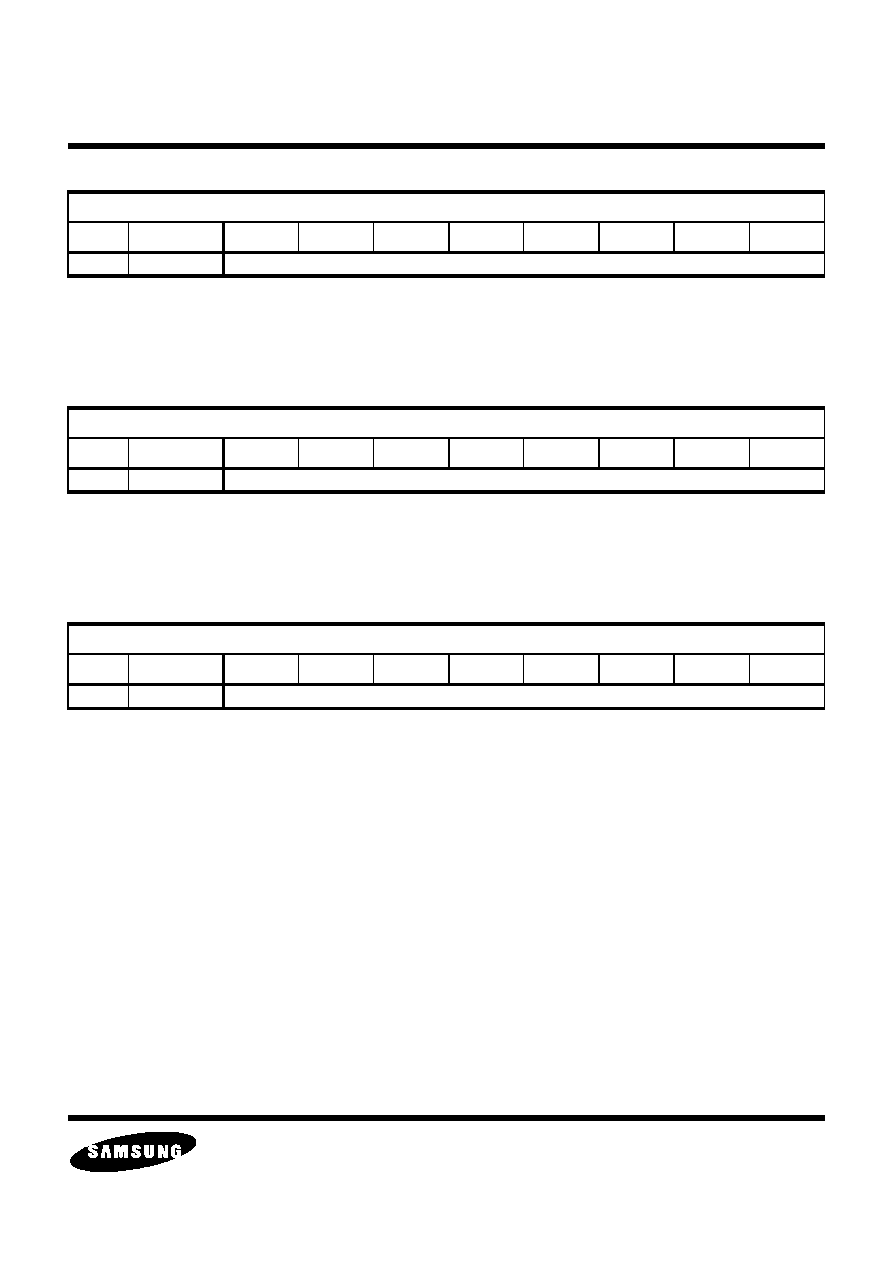
ELECTRONICS
S5D2650 Data Sheet
MULTIMEDIA VIDEO
PAGE 78 OF 95
7/18/03
Unused Y Code
Index
Mnemonic
bit 7
bit 6
bit 5
bit 4
bit 3
bit 2
bit 1
bit 0
0x35
UNUSEY
UNUSEY[7:0]
UNUSEY[7:0]
User programmed code to be output for Y data when HAV is inactive.
Unused U Code
Index
Mnemonic
bit 7
bit 6
bit 5
bit 4
bit 3
bit 2
bit 1
bit 0
0x36
UNUSEU
UNUSEU[7:0]
UNUSEU[7:0]
User programmed code to be output for U data when HAV is inactive.
Unused V Code
Index
Mnemonic
bit 7
bit 6
bit 5
bit 4
bit 3
bit 2
bit 1
bit 0
0x37
UNUSEV
UNUSEV[7:0]
UNUSEV[7:0]
User programmed code to be output for V data when HAV is inactive.

ELECTRONICS
S5D2650 Data Sheet
MULTIMEDIA VIDEO
PAGE 79 OF 95
7/18/03
Extra Control Bits for the S5D2650 Version
Index
Mnemonic
bit 7
bit 6
bit 5
bit 4
bit 3
bit 2
bit 1
bit 0
0x38
EXCTRL
PERMIN ENINCST
SLEV[1:0]
OFFST_CONT[1:0]
0
CLEVEL
CLEVEL
Programmable CKILL burst level select bit.
0
Burst peak level is 11 IRE.*
1
Burst peak level is 5.5 IRE.
OFFST_CONT
[1:0]
Y-ADC, C-ADC Offset time control
0
0.5us Y-ADC/1.0us C-ADC Offset timing
1
1.0us Y-ADC/2.0us C-ADC Offset timing*
2
2.0us Y-ADC/3.0us C-ADC Offset timing
3
3.0us Y-ADC/4.0us C-ADC Offset timing
SLEV[1:0]
HSYNC Slice level control for robust sync detection
0
Slice level fixed to 50%(Same as KS0127B)*
1
Slice level fixed to 88%
2
Slice level fixed to 25% or 75% variable, in case of input condition
3
Auto slice level based on back porch and sync tip.
ENINCST
Scaler enable control bit during VBI.
0
Scaler on during VBI interval (defined by VAV).*
1
Scaler off during VBI interval.
PERMIN
Integration time for auto slice level creation
0
Fast*
1
Slow

ELECTRONICS
S5D2650 Data Sheet
MULTIMEDIA VIDEO
PAGE 80 OF 95
7/18/03
Tracking Configuration Controls A
Index
Mnemonic
bit 7
bit 6
bit 5
bit 4
bit 3
bit 2
bit 1
bit 0
0x39
TRACKA
STCTRL MAC_DET VCR_DET
VCR_LEV[1:0]
ATCTRAP VBCTRAP AGCLSB
AGCLSB
AGC LSB for control of the 9 bit AGC gain value. This bit only write to AGC when AGCFRZ is
1.
0
Write `0' to AGC 9 bit control LSB if AGCFRZ = 1.*
1
Write `1' to AGC 9 bit control LSB if AGCFRZ = 1.
VBCTRAP
Chroma trap enabled during the VBI.
0
Chroma trap is controlled by CTRAP only.*
1
Chroma trap enabled during VBI.
ATCTRAP
Auto Chroma Trap on luma path when VCR input is detected.
0
Chroma trap is controlled by CTRAP only.*
1
If VCR type input is detected, then CTRAP is enabled.
VCR_LEV
Set the Fh variation from nominal for detection of VCR type input.
0
50 PPM.*
1
100 PPM.
2
200 PPM.
3
400 PPM.
VCR_DET
Status bit. Detect input that is not SCH locked such as consumer type VCR (Read only).
0
SCH locked video.
1
Color burst not locked to Fh (VCR).
MAC_DET
Status bit. Macrovision Encoded Data detected as input video source (Read only).
0
Standard video detected.
1
Macrovision Encoded data detected.
STCTRL
State machine transition control.
0
Normal state machine transitions.*
1
Steady state sync level removed as condition for lock.

ELECTRONICS
S5D2650 Data Sheet
MULTIMEDIA VIDEO
PAGE 81 OF 95
7/18/03
VBI Control Register B
Index
Mnemonic
bit 7
bit 6
bit 5
bit 4
bit 3
bit 2
bit 1
bit 0
0x3A
VBICTLB
VBISWAP
TT_SYS[1:0]
VBIMID
NEW_CC CC_OVFL YOFFENB COFFENB
COFFENB
Disable control for the C-path clamp control.
0
C-path clamp works as normal.*
1
C-path clamp disabled.
YOFFENB
Disable control for the Y-path clamp control.*
0
Y-path clamp works as normal.*
1
Y-path clamp disabled.
CC_OVFL
Defines when the current CCDAT1,2 data has over written previous data that was not read.
(Read Only)
0
Current data has not generated an overflow condition.
1
Current data as written over data that was not read.
NEW_CC
Defines when new Closed Caption data is ready for reading from the CCDAT1,2 bytes. (Read
Only)
0
Current data in CCDAT1,2 has already been read.
1
Current data in CCDAT1,2 is new.
VBIMID
Changes function of WSS enable (per line bases during VBI) to a raw CVBS enable.
0
When VBIL(0-15) = 3, current line is enabled for WSS slicing.*
1
When VBIL(0-15) = 3, current line is enabled for raw ADC output.
TT_SYS
Select Teletext input system when auto detect is not possible.
0
Auto Teletext Select.*
1
Teletext System B.
2
Teletext System C.
3
Teletext System D.
VBISWAP
Reverse the bit order for data output from the closed caption or Teletext slicer.
0
Same as KS0127 -- First bit sliced is located in MSB position.*
1
First bit sliced (in time) is located in LSB position.

ELECTRONICS
S5D2650 Data Sheet
MULTIMEDIA VIDEO
PAGE 82 OF 95
7/18/03
Tracking Configuration Controls B
Index
Mnemonic
bit 7
bit 6
bit 5
bit 4
bit 3
bit 2
bit 1
bit 0
0x3B
TRACKB
ALT656
VBI_PH
VBI_FR
PH_CTRL VNOISCT
AGC_LPG[1:0]
AGC_LKG
AGC_LKG
AGC gain tracking loop time constant for initial tracking mode.
0
Same as steady state time constant.*
1
2X faster than selected steady state time constant.
AGC_LPG
AGC gain steady state tracking loop time constant.
0
Fastest.*
1
Fast.
2
Slow.
3
Slowest.
VNOISCT
Vertical sync noise control enable.
0
Vertical sync adjusts with all sync phase changes.*
1
Vertical sync large phase errors must occur for 4 lines to activate a phase change.
PH_CTRL
Controls phase detector response.
0
Syncs after the "0" point reference have priority.*
1
Syncs prior to "0" point reference have priority.
VBI_FR
Disables frequency compensation for VCR head switch lines only.
0
Frequency tracking independent of this control.*
1
Frequency tracking disabled for VCR head switch lines.
VBI_PH
Enables phase compensation for VCR head switch lines only.
0
Phase tracking independent of this control.*
1
Phase tracking enabled for VCR head switch lines only.
ALT656
Alternate 656 Vertical blank location for 50 Hz video.
0
Vertical blank size per the ITU 656 Specification (ends at 656 digital line 23).*
1
Vertical blank size same as 60 Hz (ends at 656 digital line (50 Hz) 6).

ELECTRONICS
S5D2650 Data Sheet
MULTIMEDIA VIDEO
PAGE 83 OF 95
7/18/03
RTC Genlock output signal control
Index
Mnemonic
bit 7
bit 6
bit 5
bit 4
bit 3
bit 2
bit 1
bit 0
0x3C
RTC
RTC_DTO RTC_PID SEC_POL TDMOD
VCO_BIAS[1:0]
PUMP_BIAS[1:0]
PUMP_BIAS
[1:0]
PLL Block Charge Pump bias current control
VCO_BIAS[1:0]
PLL Block VCO bias current control
TDMOD
Test bit for chroma demodulation mode.
0
Normal operation.*
1
Test mode.
SEC_POL
SECAM ID Polarity Control
0
Normal*
1
Inversion
RTC_PID
Polarity control for PAL ID transferred within the RTC data stream.
0
Same polarity as default PID pin.*
1
Inverted polarity.
RTC_DTO
Enables a DTO reset inside the S5D2650 and sends a DTO reset within the RTC data stream.
Function is activated on the rising edge of RTC_DTO.
0
Function disabled.*
1
Function enabled one time when set to 1.

ELECTRONICS
S5D2650 Data Sheet
MULTIMEDIA VIDEO
PAGE 84 OF 95
7/18/03
Command Register E
Index
Mnemonic
bit 7
bit 6
bit 5
bit 4
bit 3
bit 2
bit 1
bit 0
0x3D
CMDE
ODFST
VSALG
HCORE[1:0]
CHIPREVID
CHIPREVID
Four additional bits for determination of current Revision and differentiation from the S5D2650
0
KS0127B
C
S5D2650
HCORE
Luma path horizontal coring. Noise limiter for high frequency portion of luma.
0
Coring function is disabled.*
1
1 bit of coring.
2
2 bits of coring.
3
4 bits of coring.
VSALG
Vertical scaling line dropping algorithm.
0
Vertical scaling drops the same lines in the Odd and Even fields -- good for fast
motion video.*
1
Vertical scaling drops lines based on the final de-interlaced video. This is a better
vertical scaling but may be sensitive to fast motion video.
ODFST
Alternate the first scaling line between Odd and Even fields.
0
Even field is the first scaled field.*
1
Odd field is the first scaled field.

ELECTRONICS
S5D2650 Data Sheet
MULTIMEDIA VIDEO
PAGE 85 OF 95
7/18/03
VS Delay Control
Index
Mnemonic
bit 7
bit 6
bit 5
bit 4
bit 3
bit 2
bit 1
bit 0
0x3E
VSDEL
TR_MS
NOVIDC
VSDEL[5:0]
VSDEL[5:0]
When the chip is programmed for digital video input operation, this register provides an offset
for the internal line counter to align with input video (VS can be either from the VS pin or from
embedded timing code). The register content is unsigned.
NOVIDC
Allows NOVID bit to be output to PORTB (pin 24).
0
Normal operation.*
1
The NOVID bit is output to PORTB if DATAB[2:0]=1 and DIRB=1.
TR_MS
Enable alternative initial tracking mode state machine.
0
Normal operation - Horizontal tracking mode is controlled by the HFSEL[1:0] bits.*
1
Variable tracking modes during locking time.

ELECTRONICS
S5D2650 Data Sheet
MULTIMEDIA VIDEO
PAGE 86 OF 95
7/18/03
Command Register F
Index
Mnemonic
bit 7
bit 6
bit 5
bit 4
bit 3
bit 2
bit 1
bit 0
0x3F
CMDF
CTRAPFSC
VIPMODE
EVAVY
UVDLEN
UVDLSL
REGUD
TASKB
CBWI
CBWI
Chroma bandwidth increase. This function should be used for digital video input mode only.
0
Normal chroma bandwidth.*
1
Increased chroma bandwidth.
TASKB
Select between task A and B as described in "VIP Specification V. 1.0".
0
Select CCIR 656 timing codes (T-bit is always 1).*
1
Select between task A and B when VBI data is output. If active video is output, T-bit
is set to 1(task A). If VBI data is output, T-bit is set to 0 (task B).
REGUD
Control register update control.
0
Registers are updated immediately after being written to.*
1
The following registers and register bits are updated only during the start of vertical
sync after they are written to:
Index 0x02, indices 0x17 through 0x1D, bit 0 of index 0x04, bits [2:0] and [6:4] of
index 0x0E.
UVDLSL
U or V delay control when UVDLEN is set to 1.
0
V is delayed by 1 CK period.*
1
U is delayed by 1 CK period.
UVDLEN
Enable the function of UVDLSL.
0
UVDLSL is disabled.*
1
UVDLSL is enabled.
EVAVY
Control the output of INVALY, INVALU, and INVALV codes when EVAV is inactive.
0
Output of these codes are not affected by EVAV.*
1
These codes are output when EVAV is inactive (line is being dropped by the vertical
scaler).
VIPMODE
Allows transfer of hardware sliced VBI data as ancillary data during the following line's
horizontal blanking period.
0
Standard S5D2650 original sliced VBI data transfer.*
1
Optional ancillary sliced VBI data transfer.
CTRAPFSC
Enable chroma trap location based on Fsc frequency instead of field rate.
0
Chroma trap based on field rate.*
1
Chroma trap based on detected Fsc frequency.
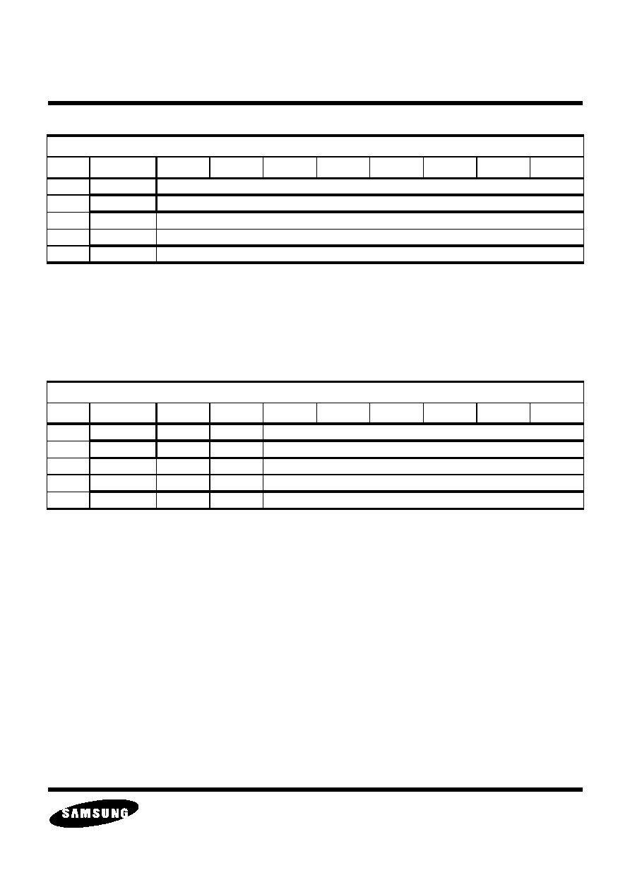
ELECTRONICS
S5D2650 Data Sheet
MULTIMEDIA VIDEO
PAGE 87 OF 95
7/18/03
Gamma Base
Index
Mnemonic
bit 7
bit 6
bit 5
bit 4
bit 3
bit 2
bit 1
bit 0
0x40
GAMMA0
GAMMA0[7:0]
0x41
GAMMA1
GAMMA1[7:0]
:
:
:
:
:
:
0x5F
GAMMA31
GAMMA31[7:0]
GAMMA0
-GAMMA31
Gamma correction base. The desired output for 8*N, where N = 0, .., 31, is programmed into
GAMMAN. Note that data written into these addresses are simultaneously written into
addresses 0xC0 through 0xDF.
Gamma Correction Delta
Index
Mnemonic
bit 7
bit 6
bit 5
bit 4
bit 3
bit 2
bit 1
bit 0
0x60
GAMMAD0
-
-
GAMMAD0[5:0]
0x61
GAMMAD1
-
-
GAMMAD1[5:0]
:
:
:
:
:
:
:
:
:
:
0x7F
GAMMAD31
-
-
GAMMAD31[5:0]
GAMMAD0
..GAMMAD31
The Nth location of the 32 locations is programmed with a 6-bit unsigned number which
represents the gamma correction delta for the gamma bases N and N + 1. The last location
will contain the gamma correction delta for gamma base 31 and presumed base 32 which has
the value of 256. Note that data written into these addresses are simultaneously written into
addresses 0xE0 through 0xFF.
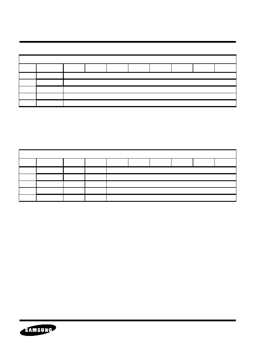
ELECTRONICS
S5D2650 Data Sheet
MULTIMEDIA VIDEO
PAGE 88 OF 95
7/18/03
U/V Gamma Base
Index
Mnemonic
bit 7
bit 6
bit 5
bit 4
bit 3
bit 2
bit 1
bit 0
0xC0
GAMUV0
GAMUV0[7:0]
0xC1
GAMUV1
GAMUV1[7:0]
:
:
:
:
:
:
0xDF
GAMUV31
GAMUV31[7:0]
GAMUV0
-GAMUV31
U and V gamma correction base. The desired output for 8*N, where N = 0, .., 31, is
programmed into GAMUVN.
U/V Gamma Correction Delta
Index
Mnemonic
bit 7
bit 6
bit 5
bit 4
bit 3
bit 2
bit 1
bit 0
0xE0
GAMUVD0
-
-
GAMUVD0[5:0]
0xE1
GAMUVD1
-
-
GAMUVD1[5:0]
:
:
:
:
:
:
:
:
:
:
0xFF
GAMUVD31
-
-
GAMUVD31[5:0]
GAMUVD0
..GAMUVD31
U and V gamma correction delta. The Nth location of the 32 locations is programmed with a
6-bit unsigned number which represents the gamma correction delta for the gamma bases N
and N + 1. The last location will contain the gamma correction delta for gamma base 31 and
presumed base 32 which has the value of 256.
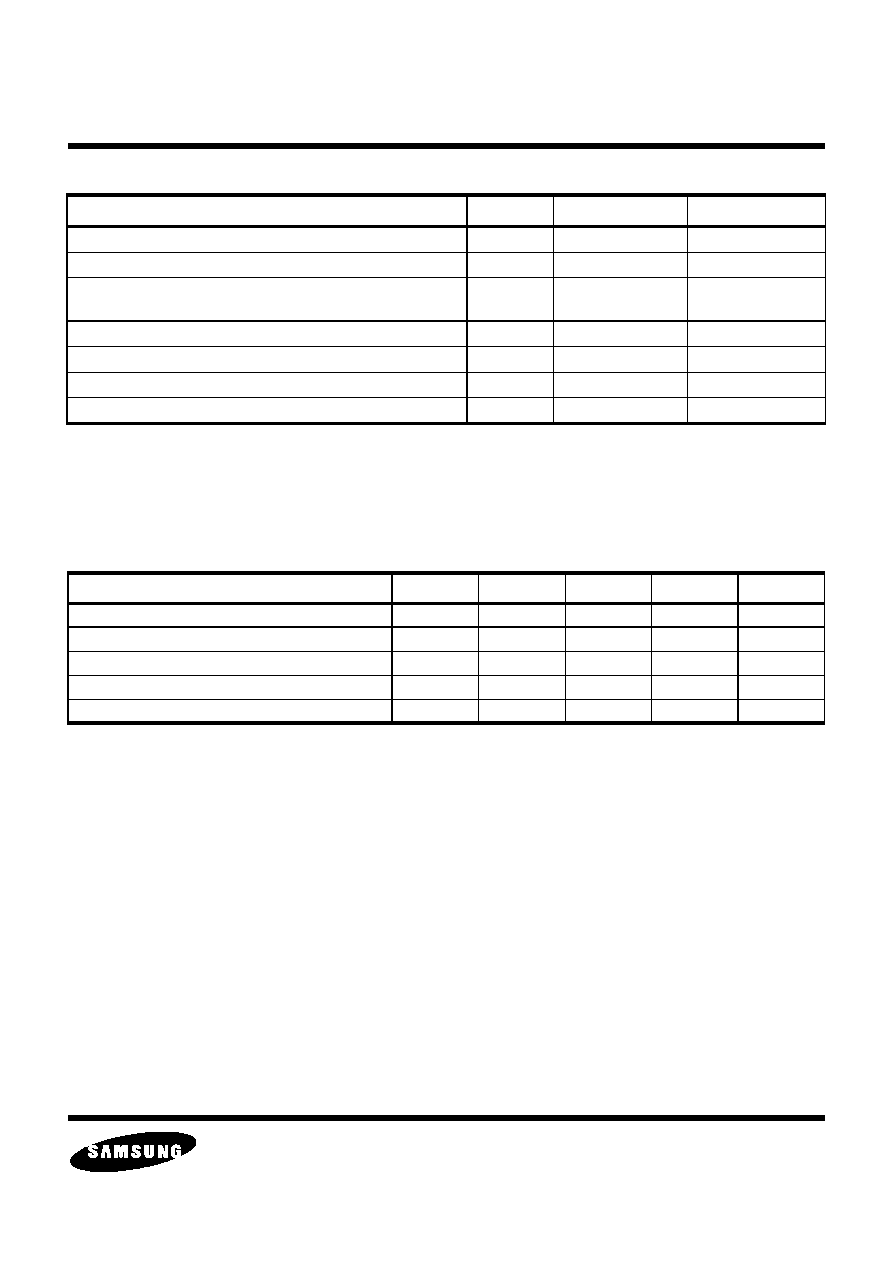
ELECTRONICS
S5D2650 Data Sheet
MULTIMEDIA VIDEO
PAGE 89 OF 95
7/18/03
ABSOLUTE MAXIMUM RATINGS
Notes: 1.Absolute maximum ratings are limiting values applied individually while all other parameters are within
specified operating conditions.
2.Functional operation under any of these conditions is not implied.
3.Applied voltage must be current limited to a specified range.
OPERATING CONDITIONS
Characteristics
Symbol
Value
Units
3.3-V supply voltage (measured to VSS)
V
DD3
-0.5 to + 3.8
V
1.8-V supply voltage (measured to VSS)
V
DD1
-0.5 to + 2.7
V
Voltage on any digital pin
V
PIN
-0.5 to
(V
DD3
+0.5)
V
Ambient operating temperature (case)
T
A
-40 to + 100
°C
Storage temperature
T
S
-65 to + 150
°C
Junction temperature
T
J
150
°C
Vapor phase soldering (1 min.)
Tvsol
220
°C
Characteristics
Symbol
Min
Typ
Max
Units
3.3-V supply voltage (measured to VSS)
V
DD3
3.0
3.3
3.6
V
1.8-V supply voltage (measured to VSS)
V
DD1
1.65
1.8
1.95
V
Thermal Impedance (case to ambient)
J
A
60
°C/W
Thermal Impedance (junction to case)
J
C
12
°C/W
Ambient operating temperature, still air
T
A
0
70
°C
ELECTRONICS
S5D2650 Data Sheet
MULTIMEDIA VIDEO
PAGE 90 OF 95
7/18/03
ELECTRICAL CHARACTERISTICS
Characteristics
Symbol
Min
Typ
Max
Units
Supply
+3.3V (Analog+I/O Buffer), normal operation
I
DD3
*1
90
*2
120
*3
150
mA
+1.8V (Digital Core), normal operation
I
DD1
40
mA
+3V (Analog+I/O Buffer), power down mode
I
DD3
*4
32
mA
+1.8V (Digital Core), power down mode
I
DD1
*4
6
mA
Analog Characteristics
Integral linearity error (AGC/ADC only)
E
I-ADC
1.0 lsb
Differential linearity error (AGC/ADC only)
E
D-ADC
0.5 lsb
Total harmonic distortion (4 MHz full scale)
THD
54
dB
Signal to noise ratio (4 MHz full scale)
SNR
42
dB
Analog bandwidth (50 IRE to 3 dB point)
BW
4
MHz
Input voltage range (peak-peak) 100 IRE input
VI(PP)
0.5
1.5
V
pp
Input resistance AY0-ACB1
R
IN
200
k
Input capacitance for analog video inputs
C
IN
10
pF
Charge current for offset control
I
OFF
±4
µ
A
Cross talk between analog inputs
a
-42
-50
dB
Video Performance
Luminance frequency response (maximum
variation to 4.2 MHz - multi burst)
F
LUMA
1.5
dB
Differential gain - complete chip (Modulated 40
IRE ramp)
D
G
1.5
%
Differential phase - complete chip (Modulated
40 IRE ramp)
D
P
1.0
degree
Chrominance frequency response (3 dB point) -
CBWR=0/1
F
CHROMA
800/500
kHz
Chroma nonlinear gain distortion (NTC-7
Combination)
C
NGD
1
%
Chroma nonlinear phase distortion (NTC-7
Combination)
C
NPD
1.25
degree
Chroma to luma intermodulation (NTC-7
Combination)
C
LI
1
IRE
Chroma luma gain equality (NTC-7 Composite) DEL
CL
±20
ns
Chroma luma delay equality (NTC-7 Composite) AMP
CL
98-101
%
Noise level for unified weighting 10 kHz-5 MHz
(100 IRE unmodulated ramp)
N
LUMA
-58
dB
Chroma AM noise (red field)
N
CAM
-60
dB
Chroma PM noise (red field)
N
CPM
-54
dB
ELECTRONICS
S5D2650 Data Sheet
MULTIMEDIA VIDEO
PAGE 91 OF 95
7/18/03
Digital I/O Characteristics
Input low voltage
V
IL
0.8
V
Input high voltage
V
IH
2.0
V
Schmitt trigger, negative going threshold
(SCLK,SDAT)
VT-
0.8
V
Schmitt trigger, positive going threshold
(SCLK,SDAT)
VT+
2.0
V
Input low current (V
IN
= VSS)
I
IL
-10
+10
µ
A
Input high current(V
IN
= VDD)
I
IH
-10
+10
µ
A
Digital output low voltage (I
OL
=1~24mA)
V
OL
0.4
V
Digital output high voltage (I
OH
=-1 ~ -24mA)
V
OH
2.4
V
three-state output leakage current
I
OZ
-10
10
µ
A
Digital output capacitance
C
OUT
7
pF
Maximum capacitance load for digital data pins C
L-DATA
30
pF
Maximum capacitance load for CK and CK2
outputs
C
L-CK
60
pF
Timing Characteristics - Digital Inputs
XTALI input pulse width low
t
pwlX
15
20
ns
XTALI input pulse width high
t
pwhX
15
20
ns
Clock and Data Timing
Analog video input to digital video output delay
t
dCHIP
120
CK
Pulse width high for CK
t
pwhCK
15
18.5
22
ns
Pulse width high for CK2
t
pwhCK2
30
37
44
ns
Delay from rising edge of CK to CK2
t
CK2
4
ns
Delay from rising edge CK to data change
(including pins Y0-Y7, C0-C7, HAV, VAV, EHAV,
EVAV, HS1, HS2, VS, ODD, PID, SCH)
t
dD
(CK is output)
7
ns
t
dD
(CK is input)
7
ns
Minimum hold time from rising edge of CK for
data output)
t
hD
0.3
ns
Timing Characteristics -IIC Host Interface
SCLK clock frequency
r
SCLK
0
400
kHz
Capacitive load for each bus line
C
b
400
pF
Hold time for START condition
t
hSTA
0.6
µ
s
Setup time for STOP condition
t
sSTO
0.6
µ
s
Rise and fall times for SCLK and SDAT
t
R
, t
F
20
300
ns
SCLK minimum pulse width low
t
pwlSCLK
1.3
µ
s
SCLK minimum pulse width high
t
pwhSCLK
0.6
µ
s
SDAT setup time to rising edge of SCLK
ts
SDAT
100
ns
Characteristics
Symbol
Min
Typ
Max
Units

ELECTRONICS
S5D2650 Data Sheet
MULTIMEDIA VIDEO
PAGE 92 OF 95
7/18/03
SDAT hold time from rising edge of SCLK
t
hSDAT
0
ns
Note: AC/DC characteristics provided are per design specifications.
Note *1 : In case of CVBS Input Mode
Note *2 : In case of S-Video Input Mode
Note *3 : In case of Component Input Mode
Note *4 : In case of Power Down Mode, I2C interface is still alive.
Characteristics
Symbol
Min
Typ
Max
Units
ELECTRONICS
S5D2650 Data Sheet
MULTIMEDIA VIDEO
PAGE 93 OF 95
7/18/03
Figure 41. Data Output
Figure 42. Analog Video Input to Digital Video Output Delay
Figure 43. IIC Host Interface Detailed Timing
t
pwhCK2
t
emT
t
f
Y,C,HAV
VAV,HS,VS
ODD,PID,
EHAV,
EVAV
CK2
t
pwhCK
CK
t
f
Blank
Analog Video
Input
Digital Video
Output
Active video
Active video
t
dCHIP
SDAT
SCLK
t
BUF
t
sSDAT
t
pwlSCLK
t
pwhSCLK
t
F
t
R
t
hSDA
t
sSTO
t
hSDAT
ELECTRONICS
S5D2650 Data Sheet
MULTIMEDIA VIDEO
PAGE 94 OF 95
7/18/03
Application Circuit
S5D2650X
VDD3
VDDD
VDDA
VDDB
VDDP
VDD1
VDD1
VDD3
VDD1
VDD1
VDD3
VDD1
VDD1
A Y 0
A Y 1
A C R 0
A C R 1
A C B 0
A C B 1
Y 7
Y 6
Y 5
Y 4
Y 3
Y 2
Y 1
Y 0
C 7
C 6
C 5
C 4
C 3
C 2
C 1
C 0
V A V
E V A V
E H A V
P I D
C K
C K 2
O D D
V S
H A V
H S 1
C C D A T
C C E N
3
4
5
1 7
1 8
2 1
2 2
2 3
2 5
2 6
7 3
7 4
4 4
3 9
3 8
3 7
3 6
3 5
3 4
3 3
5 6
5 5
5 4
5 3
4 8
4 7
4 6
4 5
8 4
8 6
8 8
9 0
9 2
9 4
T E S T 1
3 0
0 . 1 u F
V C C
FE.BEAD
1 . 8 V
9
85
89
93
98
11
12
20
42
43
59
66
67
To Frame Buffer Controller
To Frame Buffer
Analog Video Input
VSS
VSS
VSS
VSS
VSS
VSS
VSS
VSS
VSS
VSS
VSS
VSS
VSS
13
40
91
VSS
S C L K
S D A T
A E X 0
A E X 1
7 5
7 2
6 9
7 0
IIC Interface
T E S T 0
2 9
S C A N E N
3 1
T E S T 2 5 7
H S 2 7 6
C O M P 2
9 7
1 0 u F
7 5
X T A L I
X T A L O
8
7
2 4 . 5 7 6 M H z
2 2 p F
2 2 p F
E X V [ 7 : 0 ]
S C H ( P O R T B )
P O R T A
2 4
5 8
O E N
1 5
V C C
R S T B
1 0
C K E
3 2
1 0 K
1 3 . 5 M H z
6
14
19
41
60
64
65
83
87
95
96
2
1
VSS
VSS
50
49
VSS
VSS
52
51
VSS
VSS
77
78
79
80
VSS
VSS
82
81
VSS
VSS
VSS
VSS
100
VSS
0 . 1 u F
1 0 K
0 . 1 u F
FILT
9 9
1 0 p F
5 n F
8 0 K
ELECTRONICS
S5D2650 Data Sheet
MULTIMEDIA VIDEO
PAGE 95 OF 95
7/18/03
Package Dimension
Document Outline
- MULTISTANDARD VIDEO DECODER/SCALER
- FEATURES
- APPLICATIONS
- RELATED PRODUCTS
- BLOCK DIAGRAM
- PIN ASSIGNMENT - 100 PQFP
- I
- I
- I
- I
- I
- I
- O
- O
- I
- O
- I
- O
- I/O
- I/O
- O
- I/O
- O
- O
- O
- O
- O
- O
- I
- I/O
- O
- O
- O
- I/O
- I/O
- I
- I/O
- I
- 3.3V
- 1.8V
- 3.3V
- 3.3V
- GND
- GND
- I
- I
- I
- I
- I
- 1
- VSS
- 26
- HS1
- 51
- VSS
- 76
- HS2
- 2
- VSS
- 27
- EXV1
- 52
- VSS
- 77
- VSS
- 3
- VAV
- 28
- EXV2
- 53
- Y4
- 78
- VSS
- 4
- EVAV
- 29
- TEST0
- 54
- Y5
- 79
- VSS
- 5
- EHAV
- 30
- TEST1
- 55
- Y6
- 80
- VSS
- 6
- VSS
- 31
- SCANEN
- 56
- Y7
- 81
- VSS
- 7
- XTALI
- 32
- CKE
- 57
- TEST2
- 82
- VSS
- 8
- XTALO
- 33
- C0
- 58
- PORTA
- 83
- VSS
- 9
- VDD3
- 34
- C1
- 59
- VDD3
- 84
- AY0
- 10
- RST
- 35
- C2
- 60
- VSS
- 85
- VDDA
- 11
- VDD1
- 36
- C3
- 61
- EXV3
- 86
- AY1
- 12
- VDD1
- 37
- C4
- 62
- EXV4
- 87
- VSS
- 13
- VSS
- 38
- C5
- 63
- EXV5
- 88
- ACR0
- 14
- VSS
- 39
- C6
- 64
- VSS
- 89
- VDDA
- 15
- OEN
- 40
- VSS
- 65
- VSS
- 90
- ACR1
- 16
- EXV0
- 41
- VSS
- 66
- VDD1
- 91
- VSS
- 17
- PID
- 42
- VDD1
- 67
- VDD1
- 92
- ACB0
- 18
- CK
- 43
- VDD1
- 68
- EXV6
- 93
- VDDA
- 19
- VSS
- 44
- C7
- 69
- AEX0
- 94
- ACB1
- 20
- VDD3
- 45
- Y0
- 70
- AEX1
- 95
- VSS
- 21
- CK2
- 46
- Y1
- 71
- EXV7
- 96
- VSS
- 22
- ODD
- 47
- Y2
- 72
- SDAT
- 97
- COMP2
- 23
- VS
- 48
- Y3
- 73
- CCDAT
- 98
- VDDP
- 24
- PORTB(SCH)
- 49
- VSS
- 74
- CCEN
- 99
- FILT
- 25
- HAV
- 50
- VSS
- 75
- SCLK
- 100
- VSSP
- 1. FUNCTIONAL DESCRIPTION
- 1.1. VIDEO INPUT
- 1.1.1. Analog Video Input
- Figure 1. Analog Front End
- Figure 2. Typical Analog Video Input
- Table 1: Analog Video Input selections
- 0
- AY0
- Composite
- 1
- AY1
- Composite
- 2
- ACR0
- Composite
- 3
- ACR1
- Composite
- 4
- AY0,ACB0
- S-Video
- 5
- AY1,ACB1
- S-Video
- 6
- AY0,ACB0,ACR0
- YPbPr component video
- 7
- AY1,ACB1,ACR1
- YPbPr component video
- CKDIR*1
- SYNDIR*2
- EAV*3
- VMEN
- TSTGPH
- TSTGEN
- TSTGFR
- PIXSEL
- MNFMT
- IFMT
- 0
- 0
- 0
- 1
- 0
- 1
- 3
- 1
- 0
- 0
- 1
- 0
- 1
- 1
- 3
- 1
- 0
- 1
- 0
- 0
- 1
- 1
- 1
- 1
- 1
- 0
- 0
- 1
- 0
- 1
- 3
- 1
- 1
- 0
- 1
- 0
- 1
- 1
- 1
- 1
- 1
- 1
- 0
- 0
- 1
- 1
- 1
- 1
- 60
- 50
- 60
- 50
- Hz
- 858
- 864
- 780
- 944
- Pixels
- 720
- 720
- 640
- 768
- Pixels
- 480
- 580
- 480
- 580
- Lines
- 13.5
- 13.5
- 12.27
- 14.75
- MHz
- 27
- 27
- 24.54
- 29.5
- MHz
- 120
- 120
- 120
- 120
- SYG
- 72
- 72
- 72
- 72
- BPG
- [157 232]
- [139 214]
- [164 244]
- [178 264]
- CBG
- 222
- 204
- 234
- 254
- CBGW
- [159 254]
- [147 233]
- [173 254]
- [186 277]
- FH2
- 40, 900
- 42, 822
- 42, 906
- 42, 986
- COFF
- [72 232]
- [72 214]
- [72 244]
- [72 264]
- HS1
- [24 222]
- [24 204]
- [24 234]
- [24 254]
- HAV
- [293 17]
- [276 0]
- [321 33]
- [357 1]
- 109
- 255
- 255
- 109
- 255
- 255
- 117
- 255
- 255
- 100
- 240
- 235
- 100
- 240
- 235
- 100
- 229
- 235
- 7.5
- 83
- 16
- 0
- 70
- 16
- 0
- 70
- 16
- 0
- 70
- 1
- 0
- 70
- 16
- 0
- 70
- -40
- 2
- 1
- -40
- 2
- 1
- -43
- 2
- 235
- 235
- 255
- 255
- 16
- 16
- 0
- 0
- VBIL0
- VBIL1
- 9&10
- 272&273
- 6&7
- 319&320
- VBIL2
- 11
- 274
- 8
- 321
- VBIL3
- 12
- 275
- 9
- 322
- VBIL4
- 13
- 276
- 10
- 323
- VBIL5
- 14
- 277
- 11
- 324
- VBIL6
- 15
- 278
- 12
- 325
- VBIL7
- 16
- 279
- 13
- 326
- VBIL8
- 17
- 280
- 14
- 327
- VBIL9
- 18
- 281
- 15
- 328
- VBIL10
- 19
- 282
- 16
- 329
- VBIL11
- 20
- 283
- 17
- 330
- VBIL12
- 21
- 284
- 18
- 331
- VBIL13
- 22
- 285
- 19
- 332
- VBIL14
- 23
- 286
- 20
- 333
- VBIL15
- 24&25
- 287&288
- 21&22
- 334&335
- 0
- 0
- 53
- 1
- 53
- 20
- 2
- 73
- 14
- 3
- 87
- 12
- 4
- 99
- 11
- 5
- 110
- 10
- 6
- 120
- 8
- 7
- 128
- 8
- 8
- 136
- 8
- 9
- 144
- 7
- A
- 151
- 7
- B
- 158
- 6
- C
- 164
- 6
- D
- 170
- 6
- E
- 176
- 5
- F
- 181
- 6
- 10
- 187
- 5
- 11
- 192
- 5
- 12
- 197
- 5
- 13
- 202
- 5
- 14
- 207
- 4
- 15
- 211
- 5
- 16
- 216
- 4
- 17
- 220
- 5
- 18
- 225
- 4
- 19
- 229
- 4
- 1A
- 233
- 4
- 1B
- 237
- 4
- 1C
- 241
- 4
- 1D
- 245
- 4
- 1E
- 249
- 3
- 1F
- 252
- 4
- INVALY
- INVALU
- INVALV
- UNUSEY
- UNUSEU
- UNUSEV
- 2. CONTROL REGISTER DESCRIPTION