 | –≠–ª–µ–∫—Ç—Ä–æ–Ω–Ω—ã–π –∫–æ–º–ø–æ–Ω–µ–Ω—Ç: LA8519M | –°–∫–∞—á–∞—Ç—å:  PDF PDF  ZIP ZIP |
Any and all SANYO products described or contained herein do not have specifications that can handle
applications that require extremely high levels of reliability, such as life-support systems, aircraft's
control systems, or other applications whose failure can be reasonably expected to result in serious
physical and/or material damage. Consult with your SANYO representative nearest you before using
any SANYO products described or contained herein in such applications.
SANYO assumes no responsibility for equipment failures that result from using products at values that
exceed, even momentarily, rated values (such as maximum ratings, operating condition ranges, or other
parameters) listed in products specifications of any and all SANYO products described or contained
herein.
Overview
The LA8519M is a cordless telephone base unit IC that
provides I/O switching, voice signal processing, and other
functions. It integrates, on a single chip, crosspoint switch,
power amplifier, electronic volume and tone control,
microphone amplifier, speech network, and other
functions.
Functions
∑ Speech network block
-- Impedance matching, 2-wire/4-wire converter,
line driver, BN circuit network switching circuit,
transmitter amplifier, BTL receiver amplifier,
DTMF input, key tone input, receiver volume
level switching, and power supply switching
circuit.
∑ Audio signal-processing block
-- Power amplifier, electronic volume and tone
control, preamplifier with ALC, voice level
detection (VOX), beep tone input, ring tone
(OSC) input, ring tone level switching, line
volume level switching, microphone amplifier,
crosspoint switch (10
◊
9 point equivalent), and
serial interface.
Features
∑ Allows switching between two anti-sidetone networks
(near terminal/far terminal) depending on the line
current, and thus achieves excellent sidetone
characteristics over a wide range of line currents.
∑ Built-in transmitter/receiver amplifier driver power
supply switching circuit allows communication using
extension without power from the telephone network.
∑ The receiver amplifier supports both ceramic receivers
(BTL) and dynamic receiver (single).
∑ Built-in power amplifier (load: 8 to 32
): V
CC
= 5 V,
R
L
= 8
, Pomax = 200 mW
∑ The power amplifier signal path includes an electronic
volume control (7 steps of about 3.8 dB each)
∑ Includes a 10-input/9-output crosspoint switch that
provides mixing functions for easy implementation of
systems that support a diverse range of signal path
switching functions.
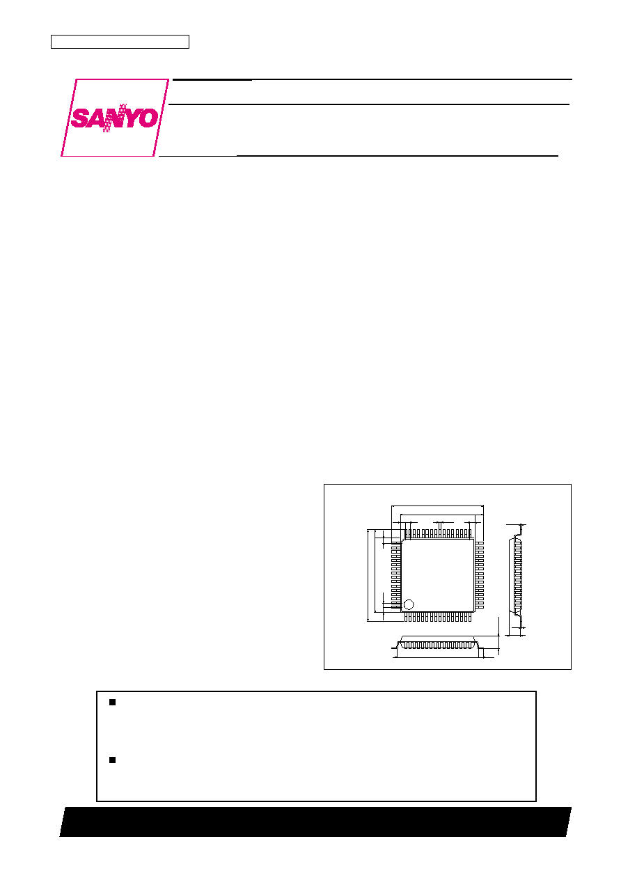
Package Dimensions
Unit:mm
3159-QIP64E
Monolithic Linear IC
Ordering number : ENN6471
N3000RM (OT) No. 6471-1/29
SANYO Electric Co.,Ltd. Semiconductor Company
TOKYO OFFICE Tokyo Bldg., 1-10, 1 Chome, Ueno, Taito-ku, TOKYO, 110-8534 JAPAN
I/O Switch/Voice Signal-Processing IC
for Cordless Telephones
LA8519M
14.0
17.2
1.0
1.0
1.6
0.15
0.35
0.1
15.6
0.8
0.8
3.0max
1
16
17
32
33
48
49
64
2.7
14.0
17.2
1.0
1.0
1.6
0.8
SANYO: QIP64E
[LA8519M]
Ratings
Parameter
Symbol
Conditions
min
typ
max
unit
[Speech Network Block] at Ta = 25∞C, Power supplied: V
CC
= 5 V, f
IN
= 1 kHz
Line voltage
V
L
1
I
L
= 20 mA
3.3
3.8
4.3
V
(20 mA, power supplied/power off)
Line voltage
V
L
2
I
L
= 50 mA
4.5
5.2
6.0
V
(50 mA, power supplied/power off)
Line voltage
EV
L
3
I
L
= 120 mA
7.1
8.5
9.9
V
(120 mA, power supplied)
Line voltage
L
V
3
I
L
= 120 mA
7.0
8.4
9.8
V
(120 mA, power off)
Transmitter gain
EGt1
I
L
= 20 mA, V
IN
= ≠55 dBV
42.5
44.5
46.5
dB
(20 mA, power supplied)
Transmitter gain
Gt1
I
L
= 20 mA, V
IN
= ≠55 dBV
42.3
44.3
46.3
dB
(20 mA, power off)
Transmitter gain
Gt2
I
L
= 120 mA, V
IN
= ≠55 dBV
38.3
40.3
42.3
dB
(120 mA, power supplied/power off)
Receiver gain
EGr1
I
L
= 20 mA, V
IN
= ≠20 dBV
≠0.9
1.1
3.1
dB
(20 mA, power supplied)
Receiver gain
EGr2
I
L
= 120 mA, V
IN
= ≠20 dBV
≠7.4
≠5.4
≠3.4
dB
(120 mA, power supplied)
Receiver gain
Gr1
I
L
= 20 mA, V
IN
= ≠20 dBV
≠5.4
≠3.4
≠1.4
dB
(20 mA, power off)
Receiver gain
Gr2
I
L
= 120 mA, V
IN
= ≠20 dBV
≠8.7
≠6.7
≠4.7
dB
(120 mA, power off)
DTMF gain
Gmf1
I
L
= 20 mA, V
IN
= ≠30 dBV
27.7
29.7
31.7
dB
(20 mA, power supplied/power off)
DTMF gain
Gmf2
I
L
= 120 mA, V
IN
= ≠30 dBV
23.6
25.6
27.6
dB
(120 mA, power supplied/power off)
KT gain (power supplied)
EGkt
I
L
= 20 mA/120 mA, V
IN
= ≠40 dBV
10.0
12.0
14.0
dB
KT gain (20 mA, power off)
Gkt1
I
L
= 20 mA, V
IN
= ≠40 dBV
5.8
7.8
9.8
dB
KT gain (120 mA, power off)
Gkt2
I
L
= 120 mA, V
IN
= ≠40 dBV
9.0
11.0
13.0
dB
Transmitter dynamic range
DRt1
I
L
= 20 mA, THD = 4%
2.5
5.6
Vp-p
(20 mA, power supplied/power off)
Transmitter dynamic range
DRt2
I
L
= 120 mA, THD = 4%
4.5
7.7
Vp-p
(120 mA, power supplied/power off)
Receiver dynamic range
EDRs
I
L
= 20 mA/120 mA, R
L
= 150
, THD = 10%
0.5
1.5
Vp-p
(power supplied)
Receiver dynamic range
DRs1
R
L
= 150
, I
L
= 20 mA, THD = 10%
0.3
0.55
Vp-p
(20 mA, power off)
Receiver dynamic range
DRs2
R
L
= 150
, I
L
= 120 mA, THD = 10%
0.5
1.4
Vp-p
(120 mA, power off)
Electrical Characteristics
Continued on next page.
No. 6471-2/29
LA8519M
Specifications
Maximum Ratings
at Ta = 25∞C
Operating Conditions
at Ta = 25∞C
Parameter
Symbol
Conditions
Ratings
Unit
Maximum supply voltage
V
CC
max
15
V
V
L
max
15
V
Line current
I
L
max
130
mA
Allowable power dissipation
Pd max
Ta
70∞C (Mounted on a glass epoxy board: 120
◊
120
◊
1.6 mm
3
)
1000
mW
Operating temperature
Topr
≠20 to +70
∞C
Storage temperature
Tstg
≠40 to +150
∞C
Parameter
Symbol
Conditions
Ratings
Unit
Recommended supply voltage
V
CC
Other than the speech network
5.0
V
Allowable operating supply voltage range
V
CC
op
Pin 17
4.5 to 6.5
V
V
CC
oppwr
Pin 28
4.5 to 9.5
V

No. 6471-3/29
LA8519M
Continued from preceding page.
Ratings
Parameter
Symbol
Conditions
min
typ
max
unit
Receiver BTL dynamic range
EDRb
I
L
= 20 mA/120 mA, R
L
= 3 k
, THD = 10%
5
10
Vp-p
(power supplied)
Receiver BTL dynamic range
DRb1
R
L
= 3 k
, I
L
= 20 mA, THD = 10%
2
3.4
Vp-p
(20 mA, power off)
Receiver BTL dynamic range
DRb2
R
L
= 3 k
, I
L
= 120 mA, THD = 10%
5
8.4
Vp-p
(120 mA, power off)
MUTE input high-level voltage
V
IH
I
L
= 20 mA to 120 mA
0.6 VSP
V
(power supplied/power off)
MUTE input low-level voltage
V
IL
I
L
= 20 mA to 120 mA
0
0.4
V
(power supplied/power off)
Transmitter PADC attenuation
Gt
I
L
= 40 mA, pin 34: grounded through 24
4.0
dB
(power supplied/power off)
Receiver PADC attenuation
Gr
I
L
= 40 mA, pin 34: grounded through 24
6.0
dB
(power supplied/power off)
Internal supply voltage
EV
SP
I
L
= 20 mA/120 mA
4.75
V
(power supplied)
Internal supply voltage
V
SP
1
I
L
= 20 mA
1.92
V
(20 mA, power off)
Internal supply voltage
V
SP
2
I
L
= 120 mA
4.74
V
(120 mA, power off)
Internal reference voltage
ES-V
REF
I
L
= 20 mA/120 mA
2.26
V
(power supplied)
Internal reference voltage
S-V
REF
1
I
L
= 20 mA
0.79
V
(20 mA, power off)
Internal reference voltage
S-V
REF
2
I
L
= 120 mA
1.92
V
(120 mA, power off)
[Voice Signal-Processing Block] at Ta = 25∞C, V
CC
= 5 V, f
IN
= 1 kHz, R
L
= 10 k
(Crosspoint switch)
Voltage gain
G
SW
V
IN
= ≠13 dBV, pin 58 input, pin 2 output
≠2.5
≠0.5
1.5
dB
Maximum input level
V
IN
max
THD = 1.5%
≠13.5
≠7.5
dBV
Output noise voltage
V
NOSW
Rg = 620
, 20 to 20 kHz
7.0
40
µVrms
(Preamplifier: input from the crosspoint switch)
Voltage gain
VG
C
V
IN
= ≠45 dBV
8.5
10.5
12.5
dB
Total harmonic distortion
THD
V
IN
= ≠20 dBV
0.26
1.0
%
ALC saturated output level
V
OS
V
IN
= ≠20 dBV
93
115
137
mVrms
ALC range
ALC
W
From the point the ALC circuit turns on to the point the THD reaches 1%.
15
dB
Output noise voltage
V
NO
Rg = 620
, 20 to 20 kHz
65
250
µVrms
(Microphone amplifier)
Voltage gain
VGm
V
IN
= ≠40 dBV
27.5
29.5
31.5
dB
Total harmonic distortion
THD
V
IN
= ≠40 dBV
0.05
1.0
%
Output noise voltage
V
NO
Rg = 620
, 20 to 20 kHz
65
250
µVrms
(Power amplifier)
Voltage gain
VGp
R
L
= 8
, V
IN
= ≠30 dBV
27.5
29.5
31.5
dB
Maximum output power
Po
R
L
= 8
, THD = 10%
200
275
mW
Total harmonic distortion
THD
V
IN
= ≠30 dBV
0.8
1.5
%
Ripple rejection ratio
SVRR
Rg = 620
, fr = 100 kHz, Vr = ≠20 dBV
40
50
dB
Output noise voltage
V
NO
Rg = 620
, 20 to 20 kHz
35
100
µVrms
(VOX)
Sensitivity 1 low level
V
OX
L
V
IN
= ≠40 dBV, R
L
= 100 k
0.1
0.3
V
Sensitivity 2 high level
V
OX
H
V
IN
= ≠44 dBV, R
L
= 100 k
4.8
4.95
V
(Electronic volume control)
Step width
Evrw
2.9
3.8
4.7
dB
(Attenuator)
R-ATT attenuation
GR
5.4
6.4
7.4
dB
LINE-ATT attenuation
GL
4.6
5.6
6.6
dB
OSC-ATT attenuation
GO
13.1
14.6
16.1
dB
Continued on next page.

No. 6471-4/29
LA8519M
Continued from preceding page.
Ratings
Parameter
Symbol
Conditions
min
typ
max
unit
(V
REF
)
Output voltage
V
REF
2.07
2.27
2.47
V
(Serial Control)
Clock frequency
Fck
500
kHz
Input signal high level
V
H
2.3
V
Input signal low level
V
L
1.0
V
(Power Supply Switching)
Pin 17 voltage 1
Vch1
The voltage applied to pin 17 is valid.
3.5
V
Pin 17 voltage 2
Vch2
The voltage supplied from pin 48 is valid.
1.0
V
Quiescent current
I
CCO
With the power amplifier on
24
33.5
mA

No. 6471-5/29
LA8519M
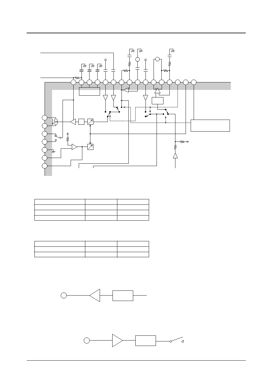
Block Diagram
1234567
0E
8
ALC
VR
SW5
91
0
OSC-ATT
0/≠16DB
≠9.5DB
≠9.5DB
ALC-OUT
BEEP-IN
OSC-IN
VOX-IN
RESET
(PWR ON RESET)
PAD C
MUTE
MIC
VREF
VOX-RCT
11
PRE
AMP
12
13
14
15
16
18
19
20
21
22
23
24
25
26
27
28
29
30
31
32
33
34
35
36
R
KT
37
38
39
40
41
42
43
44
45
46
47
48
49
50
51
52
53
54
55
56
57
58
59
60
61
62
DSP
Compander 1
Compander 2
Door phone
63
64
+
+
+
+
+
+
+
+
+
+
+
+
L-ATT
0/≠6DB
P.V
REF
REG
Electronic
volume control
V
CC
EXT.REG
Power supply
5V
PWR MONI
NC
SP
VOX OUT
CE
DATA
CLOCK
PWR-V
CC
PWR-GND
HAND
SW4
SW3
TRANSMIT-AMP
SW2
SW1
GAIN CTL
BN1
BN2
RECEIVER-AMP
Line amplifier
HAND-AMP
RF1
RF2
DOOR
CODEC1
CODEC2
FILTER
EVR
POWER
AMP
MIC
AMP
VOX
CMP
RECT
R-ATT
0/≠6DB
LINE-AMP
9.5DB
CPU
INTERFACE
17
16
1D
23
35
06
0F
2A
31
36
07
29
30
3B
0D
15
1C
22
34
3A
05
0C
14
1B
21
33
39
04
0B
13
1A
28
2F
0A
12
20
27
2E
03
09
19
1F
26
2D
02
11
18
1E
25
2C
38
01
08
10
17
24
2B
32
37
DTMF
T
1.RF1-OUT
2.RF2-OUT
3.DOOR-OUT
4.CDC1-OUT
5.CDC2-OUT
6.ALC-CNT
7.BEEP-IN
8.OSC-IN
9.GND
10.ALC-IN
11.PRE-OUT
12.PRE-NF
13.VOXA-IN
14.VOXA-OUT
15.V
REF
16.VOX-RCT
17.V
CC
18.MIC-OUT
19.MIC-NF
20.MIC-IN
21.NC
22.EVR-OUT
23.PWR-IN
24.P-V
REF
25.PWR-NF
26.P-GND
27.PWR-OUT
28.P-V
CC
29.VOX-OUT
30.CE
31.DATA
32.CLOCK
33.RESET
34.PAD-CNT
35.MUTE
36.RV-NF
37.RV-OUT1
38.RV-OUT2
39.KT-IN
40.TI-IN
41.TI-NF
42.TI-OUT
43.TA-IN
44.DTMF-IN
45.SP-V
REF
46.VSP
47.SP-V
CC
48.VL
49.TOI
50.TOO
51.BN1
52.BN2
53.SP-GND
54.RI-IN
55.RI-OUT
56.HAND-NF
57.HAND-MONI
58.RF1-IN
59.RF2-IN
60.DOOR-IN
61.FIL-IN
62.FIL-OUT
63.CDC2-IN
64.LINE-OUT
A13120
PO
WER SUPPL
Y

No. 6471-6/29
LA8519M
Test Circuit Diagram
123456789
1
0
0.1
µ
F
0.1
µ
F
SW2-2
0.1
µ
F
0.1
µ
F
0.1
µ
F
0.1
µ
F
0.1
µ
F
0.1
µ
F
0.22
µ
F
220
µ
F
1
µ
F
1
µ
F
0.1
µ
F
100
µ
F
0.01
µ
F
0.47
µ
F
10
µ
F
0.1
µ
F
0.1
µ
F
0.1
µ
F
0.1
µ
F
10
µ
F
0.22
µ
F
0.22
µ
F
0.1
µ
F
0.1
µ
F
0.1
µ
F
0.1
µ
F
0.1
µ
F
22
µ
F
47
µ
F
220
µ
F
0.1
µ
F
0.22
µ
F
DRCT-SW
220
µ
F
0.1
µ
F
0.1
µ
F
470
µ
F
100
µ
F
0.22
µ
F
0.1
µ
F
10
µ
F
220k
10k
100
k
VOX-IN-SW
100k
10k
3.3k
2k
150pF
62k
8
(1W)
OUTPUT
VOX-OUT
24k
620
51
7.5K
8.2K
5.6K
8200pF
180pF
6800pF
82
82
82
(1W)
2SA608NP
3.3k
600
(10W)
1.3k
1.8k
11k
22k
39k
47k
6.2k
300
150
3k
0.1
µ
F
20k
100
k
100
k
150
k
100
k
51k
V
CC
5V
330pF
100k
620
100
k
10k
11
12
13
14
15
16
18
19
20
21
22
23
24
25
26
27
28
29
30
31
32
33
RESET
PAD-CNT
MUTE
RV-NF
RV-OUT1
RV-OUT2
KT-IN
TI-IN
TI-NF
TI-OUT
TA-IN
DTMF-IN
SP-VREF
VSP
SP-VOC
VL
34
35
36
37
38
39
40
41
42
43
44
45
46
47
48
49
TOI
TOO
BN1
BN2
SP-GND
RI-IN
RI-OUT
HAND-NF
HAND-MONI
LA8519M
RF1-IN
RF2-IN
DOOR-IN
FIL-IN
FILOUT
CDC2-IN
LINE-OUT
50
51
52
53
54
55
56
57
58
59
60
61
62
63
64
+
+
+
+
+
+
+
+
17
V
CC
MIC-OUT
INPUT
INPUT
1kHz
620
1kHz
MIC-NF
MIC-IN
NC
EVR-OUT
PWR-IN
P-V
REF
PWR-NF
P-GND
PWR-OUT
P-V
CC
VOX-OUT
CE
DATA
CLOCK
CE
DATA
CLOCK
Data generator
47K
A13121
+
RF1-OUT
RF2-OUT
DOOR-OUT
CDC1-OUT
CDC2-OUT
ALC-CNT
BEEP-IN
OSC-IN
GND
ALC-IN
PRE-OUT
PRE-NF
VOXA-IN
VOXA-OUT
VREF
VOX-RCT
+
SW2-1
SW2-3
SW2-4
SW2-5
SW2-6
SW5-1
SW3-1
SW1-7
SW2-7
SW2-8
SW3-2
SW3-3
SW3-4
RV1
RV2
VL
SP-IN
PWR-OUT
0.45V
VCNT
IL
+
+
SW4-1
MUTE-SW
BTL-SW
RAD-C-SW
RESET-SW
+
SW4-2
SW4-3
SW4-4
SW1-6
SW1-4
SW1-2
SW1-1

No. 6471-7/29
LA8519M
Sample Application Circuit
123456789
1
0
BEEP-IN
0.1
µ
F
0.1
µ
F
0.1
µ
F
0.1
µ
F
0.1
µ
F
0.1
µ
F
0.1
µ
F
0.22
µ
F
220
µ
F
1
µ
F
1
µ
F
0.033
µ
F
220
µ
F
0.01
µ
F
0.47
µ
F
KT-IN
DTMF-IN
0.1
µ
F
0.1
µ
F
0.1
µ
F
0.1
µ
F
0.22
µ
F
0.22
µ
F
0.1
µ
F
0.1
µ
F
0.1
µ
F
0.1
µ
F
0.1
µ
F
100
µ
F
47
µ
F
220
µ
F
0.1
µ
F
0.22
µ
F
220
µ
F
0.1
µ
F
0.1
µ
F
470
µ
F
0.1
µ
F
100
µ
F
0.22
µ
F
0.1
µ
F
330pF
330pF
47
µ
F
220k
10k
330pF
3.3k
2k
62k
24k
620
51
7.5K
8.2K
8.2
5.6K
8200pF
180pF
330pF
6800pF
82
82
(1W)
2SA608NP
3.3k
1.3k
1.8k
11k
22k
10k
6.2k
0.1
µ
F
20k
51k
CPU
TIP
V
CC
5V
LINE
RING
330pF
10k
OSC-IN
MIC
11
12
13
14
15
16
18
19
20
21
22
23
24
25
26
27
28
29
30
31
32
33
RESET
PAD-CNT
MUTE
RV-NF
RV-OUT1
RV-OUT2
KT-IN
TI-IN
TI-NF
TI-OUT
TA-IN
DTMF-IN
SP-VREF
VSP
SP-VOC
VL
34
35
36
R
37
38
39
40
41
42
43
44
45
46
47
48
49
TOI
TOO
BN1
BN2
SP-GND
RI-IN
RI-OUT
HAND-NF
HAND-MONI
LA8519M
RF1-IN
RF2-IN
DOOR-IN
FIL-IN
FILOUT
CDC2-IN
LINE-OUT
50
51
52
53
54
55
56
57
58
59
60
61
62
DSP
Compander 1
Compander 2
Door phone
63
64
+
+
+
+
+
+
+
SP
FILTER
17
V
CC
MIC-OUT
MIC-NF
MIC-IN
NC
EVR-OUT
PWR-IN
P-V
REF
PWR-NF
P-GND
PWR-OUT
P-V
CC
VOX-OUT
CE
DATA
CLOCK
T
A13122
+
+
+
RF1-OUT
RF2-OUT
DOOR-OUT
CDC1-OUT
CDC2-OUT
ALC-CNT
BEEP-IN
OSC-IN
GND
ALC-IN
PRE-OUT
PRE-NF
VOXA-IN
VOXA-OUT
VREF
VOX-RCT
100
k
100
k
330
pF
100
k
100
k
150
k
100
k
100
k
100
k

Serial Data Format
No. 6471-8/29
LA8519M
Address Table
Output
LINE
HAND
RF1
RF2
DOOR
CDC1
CDC2
EVR
PRE
Input
LINE
--
08
10
17
--
24
2B
32
37
HAND
01
--
11
18
1E
25
2C
--
38
RF1
02
09
--
19
1F
26
2D
--
--
RF2
03
0A
12
--
20
27
2E
--
--
DOOR
--
0B
13
1A
--
28
2F
--
--
CDC1
04
0C
14
1B
21
--
--
33
39
CDC2
05
0D
15
1C
22
--
--
34
3A
MIC
--
--
--
--
--
29
30
--
3B
BEEP
06
0E
16
1D
23
--
--
35
--
PRE
07
0F
--
--
--
2A
31
36
--
Address No.
Mode
00
Sets all crosspoint and control switches to the off state.
*
2
3C
ALC control (D = 1: Off, D = 0: On)
3D
Transmitter/receiver control (SW1 and SW4 in the block diagram)
*
1
3E
OSC input (SW5) control (D = 1: On, D = 0: Off)
3F
Power amplifier control (D = 1: On, D = 0: Off)
40
Electronic volume control
0 dB
(Default value)
41
Electronic volume control
≠4 dB
42
Electronic volume control
≠8 dB
43
Electronic volume control
≠12 dB
*
2
44
Electronic volume control
≠16 dB
45
Electronic volume control
≠20 dB
46
Electronic volume control
≠24 dB
47
Electronic volume control
≠28 dB
7D
Line attenuator (L-ATT) setting (D = 1: ≠6 dB, D = 0: 0 dB)
7E
Receiver attenuator (R-ATT) setting (D = 1: 0 dB, D = 0: ≠6 dB)
7F
Oscillator attenuator (OSC-ATT) setting (D = 1: 0 dB, D = 0: ≠16 dB)
Other addresses
CE
CLOCK
DATA
A6
A5
A4
A3
A2
A1
A0
D
A6 to A0
Sets the address of the crosspoint switch or control switch (hexadecimal
binary number)
D
Sets the on/off state of the crosspoint switch or control switch.
(The switch is set to the on state when D is 1, and to the off state when 0.)
*
With address 3D set to the on state, SW1 is set to enable the transmitter amplifier output (pin 42) and SW4 is set to enable either the receiver amplifier
output (pin 55) or the KT (pin 39) signal. If a voltage is not supplied to V
CC
(pin 17) (i.e. the power off state), SW1 and SW4 are set to the same states
as when address 3D is set to the on state.
**
For addresses 00 and 40 to 47, the data D may be either 0 or 1.
Notes: 1. The receiver attenuator (R-ATT) is set to ≠6 dB at power on or after a reset (pin 33 set to low, or address 00 accessed).
2. The line attenuator (L-ATT) is set to 0 dB at power on or after a reset (pin 33 set to low, or address 00 accessed).
3. The oscillator attenuator (OSC-ATT) is set to ≠16 dB at power on or after a reset (pin 33 set to low, or address 00 accessed).
4. The electronic volume control is set to 0 dB at power on or after a reset (pin 33 set to low, or address 00 accessed).
5. Addresses are expressed as hexadecimal numbers.
6. Since the LA8519M includes a power on reset function, all the crosspoint and control switches are reset to their default states when external power
(pin 17: V
CC
) is applied.
7. Switches SW2 and SW3 in the block diagram are controlled by the MUTE pin (pin 35). The table lists the signals enabled by this pin.
MUTE pin (pin 35)
SW2
SW3
High/Open
Transmitter (pin 42) and TA-IN (pin 43)
Receiver (pin 55)
Low
DTMF pin (pin 44)
KT pin (pin 39)

No. 6471-9/29
LA8519M
Serial Data Timing
A1
D
CLOCK
DATA
CE
A2
A0
A3
A4
A5
A6
A6
A5
f
MAX
t
WH
t
WH
tDS tDS
t
CS
t
CH
t
WC
∑ f
MAX
(maximum clock frequency)
500 kHz
∑ t
WL
(clock low-level pulse width)
At least 1 µs
∑ t
WH
(clock high-level pulse width)
At least 1 µs
∑ t
CS
(chip enable setup time)
At least 1 µs
∑ t
CH
(chip enable hold time)
At least 1 µs
∑ t
DS
(data setup time)
At least 1 µs
∑ t
DH
(data hold time)
At least 1 µs
∑ t
WC
(chip enable pulse width)
At least 1 µs
Note: The control data must be input at least 400 ms after the supply voltage is applied to the V
CC
pin (pin 17).

Pin No.
Pin
Notes
Equivalent circuit
No. 6471-10/29
LA8519M
Pin Functions
∑ These are the IC outputs.
1
2
3
4
5
RF1-OUT
RF2-OUT
DOOR-OUT
CDC1-OUT
CDC2-OUT
V
CC
1
10 k
10 k
2
3
4
5
V
REF
CP-SW
∑ Adjusts the ALC time constants
This pin can be used to adjust the ALC attack time
and recovery time.
6
ALC-CNT
V
CC
6
∑ Beep tone amplifier input
∑ Oscillator amplifier input
∑ Compander 1 input
∑ Compander 2 input
∑ CDC2 amplifier input
7
8
58
59
63
BEEP-IN
OSC-IN
RF1-IN
RF2-IN
CDC2-IN
8
58
59
63
7
V
CC
V
REF
30 k
30 k
Signal-processing system ground
9
GND
10
V
CC
V
REF
10 k
24 k
∑ ALC input. The PRE output (pin 11) is input to this
pin through a coupling capacitor. The ALC level
can be adjusted by inserting a resistor in series.
10
ALC-IN
Continued on next page.

No. 6471-11/29
LA8519M
Continued from preceding page.
Continued on next page.
Pin No.
Pin
Notes
Equivalent circuit
∑ Preamplifier output
11
12
PRE-OUT
PRE-NF
11
V
CC
12
V
REF
∑ VOX amplifier input
∑ VOX amplifier output
13
14
VOXA-IN
VOXA-OUT
13
V
CC
V
REF
300
14
∑ Internal reference voltage output
15
VREF
5 k
V
CC
15
2.25 V
∑ External power supply input. This voltage is
supplied to the signal-processing system and V
SP
(pin 46).
17
V
CC
4.7 k
4.7 k
V
CC
16
∑ VOX detection output. This circuit can also be
used as a waveform shaping circuit by forcibly
setting this pin to the high state.
16
VOX-RCT

No. 6471-12/29
LA8519M
Continued from preceding page.
Continued on next page.
Pin No.
Pin
Notes
Equivalent circuit
∑ Microphone amplifier output
∑ Microphone amplifier minus input
∑ Microphone amplifier plus input
18
19
20
MIC-OUT
MIC-NF
MIC-IN
V
CC
20
V
RE
100 k
18
19
∑ EVR amplifier output
22
EVR-OUT
22
∑ Power amplifier plus input
∑ Power amplifier reference voltage
(about 4/9
◊
P-V
CC
)
∑ Power amplifier minus input
∑ Power amplifier output
23
24
25
27
PWR-IN
P-VREF
PWR-NF
PWR-OUT
25
27
P.V
CC
24
15 k
23
50 k
40 k
∑ Unused.
21
NC
∑ Power system ground
26
P-GND
∑ Power system power supply
28
P-V
CC
∑ VOX output
This is an open-collector output.
29
VOX-OUT
29
V
CC

No. 6471-13/29
LA8519M
Continued from preceding page.
Continued on next page.
Pin No.
Pin
Notes
Equivalent circuit
∑ Chip enable input
∑ Data input
∑ Clock input
∑ Reset
Power on reset.
30
31
32
33
CE
DATA
CLOCK
RESET
30
31
32
33
V
CC
100 k
1 k
1.5 V
Logic
∑ Pad control. The gain control based on line
current and the BN switching operating current
can be controlled by connecting this pin through a
resistor to either ground or S-V
CC
(pin 47).
34
PAD C
34
S-V
CC
22 k
4.7 k
∑ Muting control. This pin switches the transmitted
audio and DTMF signals in the transmitter system
and the KT and received signals in the receiver
system. (Switches SW2 and SW3 in the block
diagram.) When low, the DTMF and KT signals
are enabled.
35
MUTE
35
V
SP
50 k
1 k
REF
∑ Receiver amplifier noise figure connection
∑ Receiver amplifier 1 output
∑ Receiver amplifier 2 output
36
37
38
RV-NF
RV-OUT1
RV-OUT2
36
V
SP
37
10 k
10 k
REF
38
V
SP

No. 6471-14/29
LA8519M
Continued from preceding page.
Continued on next page.
Pin No.
Pin
Notes
Equivalent circuit
∑ Key tone input
39
KT-IN
44 k
V
SP
VSP
39
REF
∑ Transmitter input amplifier plus input. Since no
bias voltage is applied internally, a bias voltage
must be applied through a resistor from the REF
pin (pin 61).
∑ Transmitter input amplifier minus input
∑ Transmitter input amplifier output
40
41
42
TI-IN
TI-NF
TI-OUT
V
SP
42
V
SP
40
41
∑ Input for the line output
43
TA-IN
V
SP
43
REF
40 k
∑ DTMF input
44
DTMF-IN
20 k
V
SP
V
SP
44
REF

No. 6471-15/29
LA8519M
Continued from preceding page.
Continued on next page.
Pin No.
Pin
Notes
Equivalent circuit
∑ Speech network system internal reference voltage
output. When the V
CC
(pin 17) voltage is over
3.5 V, the reference voltage is output from V
REF
(pin 15). When the V
CC
voltage is under 1.2 V, a
voltage of about (2/5)
◊
V is output.
45
REF
V
SP
15 k
10 k
45
V
REF
∑ Speech network system internal power supply. A
voltage of about 0.3 V less than the voltage
applied to V
CC
is output when the V
CC
(pin 17)
voltage is over 3.5 V. When the V
CC
voltage is
under 1.2 V, a voltage of about 0.3 V less than the
S-V
CC
(pin 47) voltage is output.
46
VSP
∑ Speech network system power supply. When the
V
CC
voltage is under 1.2 V, power is supplied to
V
SP
(pin 46) based on the line power.
47
S-V
CC
∑ Line current input and line voltage
∑ Current input for the transmitter output current
∑ Transmitter output current output
48
49
50
VL
TOI
TOO
3 k
6.2 k
100
48
50
49
∑ First BN switching control input
∑ Second BN switching control input
Connect these inputs when two balancing
networks are used. When unused, leave these
pins open.
51
52
BN1
BN2
VL
48
52
51
∑ Speech network system ground
53
SP-GND
∑ Receiver input amplifier minus input
∑ Receiver input amplifier output
54
55
RI-IN
RI-OUT
54
V
SP
55
REF

No. 6471-16/29
LA8519M
Continued from preceding page.
Pin No.
Pin
Notes
Equivalent circuit
∑ Handset amplifier minus input
∑ Handset amplifier output
56
57
HAND-NF
HAND-MONI
56
57
V
CC
∑ Door phone input
60
DOOR-IN
V
CC
V
REF
50 k
10 k
60
∑ FIL amplifier input
∑ FIL amplifier output
61
62
FIL-IN
FIL-OUT
V
CC
V
REF
61
300
62
∑ Line amplifier output
64
LINE-OUT
64
V
CC
10 k

Usage Notes
Speech Network Circuit Block
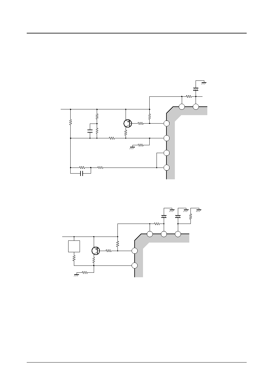
∑ External driver transistor
No. 6471-17/29
LA8519M
+
49
48
TOI
VL
S-VCC
50 TOO
LA8519M
51 BN1
52 BN2
47
7.5k
51
C1
R1
Tr
82
82
620
R3
220
µ
F
C2
3.3k
8.2
R2
8.2k
5.6k
1.3k
1.8k
8200pF
6800pF
A13123
4
5
2
3
6
7
8
9
10
11
12
10
20
30
40
50
60
70
80
90
100
110 120 130
Figure 1
Line
Since the IC includes a built-in power amplifier, due to the allowable power dissipation limits, include a heat
dissipation transistor as shown in figure 1, and dissipate the circuit current outside the IC. Set the allowable power
dissipation for R1 and R2 according to the maximum expected circuit current. (The values shown are for reference
purposes only.)
Note: If oscillation occurs due to the load state between VL and ground, insert the capacitor C1 (about 0.1 µF)
shown in the figure.
∑ Changing the DC resistance
The DC resistance can be modified by using a variable resistor for R2 in figure 1. (See the figure below.)
Note: Note that changing R2 will also change the transmitter gain and the balancing network conditions.
∑ Determining the AC impedance
The AC impedance is basically determined by R3 (620
) and C2 (220 µF) shown in figure 1 above page. Since in
actual operation there will be other AC loads in addition to the speech network, adjust the total AC impedance for
the whole system in combination with the speech network impedance.
Note: Note that if R3 is changed, the DC resistance will change as well.
Line Voltage vs. Line Current
Line current -- mA
Line
Power supplied: V
CC
= 5 V
Power supplied: R2 = 10
Power off: R2 = 10
Power supplied: R2 = 8.2
Power off: R2 = 8.2
Power supplied: R2 = 6.8
Power off: R2 = 6.8
No. 6471-18/29
LA8519M
∑ Anti-sidetone network
The LA8519M can switch between two anti-sidetone networks, one for the near terminal and one for the far
terminal, depending on the circuit current. (See figure 1 for the connections used.) The switching point can be
changed by connecting PADC (pin 34) through a resistor to either ground or S-V
CC
(pin 47).
If only one anti-sidetone network is used, short pin 51 to pin 52 as shown in figure 2. (The component values
shown are for reference purposes only.)
+
49
48
TOI
VL
S-VCC
50 TOO
LA8519M
51 BN1
52 BN2
47
6.2k
51
Tr
82
82
11k
1.5k
0.01
µ
F
620
3.3k
8.2
A13124
Line
Figure 2
∑ Line voltage VL DC characteristics when V
CC
is not applied (Values shown are for reference purposes only.)
+
49
48
TOI
VL
S-VCC
VSP
50 TOO
LA8519M
47
+
46
51
Tr
82
82
620
3.3k
8.2
A13125
BN
Load
The slope of the DC characteristics when V
CC
is not applied can be increased without changing the DC
characteristics when V
CC
is applied by applying a load to V
SP
(pin 46).
No. 6471-19/29
LA8519M
∑ Receiver amplifier application circuits
(1) When a dynamic receiver is used (Values shown are for reference purposes only.)
+
37
RV-OUT1
RV-NF
38
RV-OUT2
36
10
µ
F
0.47
µ
F
330pF
300
100k
6.2k
A13126
Due to drive capacity considerations,
a 300
resistor must be inserted in series.
∑ Receiver attenuator
37
RV-OUT1
ATT
SW4
RV-NF
38
RV-OUT2
36
A13128
Normally, the receiver attenuator is set to ≠6 dB. It can be set to 0 dB by setting address 7E to the on state with a
serial data transfer.
(2) When a ceramic receiver is used (Values shown are for reference purposes only.)
37
RV-OUT1
RV-NF
38
RV-OUT2
36
0.47
µ
F
330pF
100k
6.2k
A13127

No. 6471-20/29
LA8519M
∑ Speech network gain distribution
42
41
44
DTMF-IN
TA-IN
48
VL
40 TI-IN
43
100 k
20 k
SW2
0 dB
SW1
0 dB
A13129
*
IL = 20 mA
**
IL = 120 mA
Note: For a 600
line termination
Line driver
amplifier
30 dB
Transmitter PAD
0 dB
*
1
≠3.5 dB
*
2
Transmitter amplifier
(15.5 dB)
54
48
BN
VL
KT-IN
300
11 k
150 k
6.2 k
100 k
150
ATT
≠6.5 dB
0 dB
*
3
SW3
0 dB
SW4
4 dB
A13130
ATT
55
39
38
37
36
*
IL = 20 mA
**
IL = 120 mA
***
When address 7E is set to the on state with a serial data transfer.
Notes: 1. The gain values are rough values, and should be seen as target values during the design process.
2. Values in parentheses can be modified by external components.
Anti-sidetone
circuit
(≠33.6 dB)
Receiver input
amplifier
(22.7 dB)
Receiver PAD
0 dB
*
1
≠6.5 dB
*
2
Receiver output
amplifier
(24.7 dB)
Attenuator
(≠9.5 dB)
No. 6471-21/29
LA8519M
∑ Speech network internal analog switch operation
48
49
BN1
BN2
SW2
SW3
SW4
≠9.5 dB
HAND
SW1
2
1
2
2
1
1
1
2
TRANSMIT
AMP
GAIN CTL
RECEIVER
AMP
50
51
52
53
54
55
47
46
45
44
43
42
41
40
39
ATT
CPU
INTERFACE
Power supply
Line amplifier
T
38
37
36
35
MUTE
PAD-CNT
RESET
(PWR ON RESET)
34
33
A13131
+
+
+
R
Note: Switches SW2 and SW3 are controlled by the MUTE pin (pin 35). Switches SW1 and SW4 are controlled by address 3D as set by serial data
transfers. Note that switches SW2 and SW3 operate together, as do switches SW1 and SW4.
SW1 and SW4 Operation
State
SW1
SW4
Power supplied (initial state)
1
1
Address 3D
2
2
Power off
2
2
Note: When the power is off, SW1 and SW4 go to the "2" positions, and their states cannot be changed.
SW2 and SW3 Operation
Pin 35 (MUTE)
SW2
SW3
High
1
1
Low
2
2
Note: SW2 and SW3 operate as described above regardless of the power supplied/off state.
∑ Line amplifier attenuator
Normally, the line attenuator is set to 0 dB. It can be set to ≠6 dB by setting address to 7D and mode to D = 1 with
a serial data transfer.
LINE-OUT
ATT
64
A13132
∑ Oscillator amplifier attenuator
Normally, the oscillator amplifier attenuator is set to ≠16 dB. It can be set to 0 dB by setting address to 7F and
mode to D = 1 with a serial data transfer.
A13133
OSC-IN
ATT
SW5
8
Crosspoint Switch

No. 6471-22/29
LA8519M
∑ VOX circuit
(1) The VOX circuit detects whether there is conversation or not. When the signal level in the VOXA input block
(when the application constants in the application circuit diagram are used) becomes over about ≠42 dBV, the
VOX output pin (pin 29) goes low. The detection level can be set by setting the gain of the VOX input amplifier
with resistors R1 and R2.
(2) This circuit can be used as a waveform shaping circuit if VOX-RCT (pin 16) is connected to V
CC
, i.e. if pin 16 is
set to the high level. Thus this circuit can also be used to recognize a 400 Hz beep tone. In this mode, there is no
need to connect a capacitor to pin 16.
+
R2
R1
VREF
RECT CMP
VOX-RCT
14
13
+
≠
15
16
29
VOXA-IN
A13134
∑ Power amplifier circuit applications (The component values are for reference purposes only.)
+
+
28
C2
C1
C6
C5
SP
C3
C4
PWR-VCC
27
PWR-OUT
26
PWR-GND
25
PWR-NF
24
PWR-VREF
23
PWR-IN
22
PWR-MONI
+
0.22
µ
F
62 k
2 k
A13135
C1: 0.1 µF
C2: 0.1 µF
C3: 0.1 µF
C4: 220 µF
C5: 100 to 470 µF
C6: 220 µF
SP: 8 to 32
∑ Voltage gain: 20 to 30 dB
∑ A frequency characteristics adjustment capacitor cannot
be attached to the feedback resistor.
Note: The power amplifier output goes to the high-impedance state in the muted state,
i.e. when address 3F has been set to the off state.
∑ Power amplifier phase compensation capacitors
Of the external components, the capacitors C1 between pin 27 (output) and pin 26 (ground) and C2 between pin 27
and pin 28 (V
CC
) are power amplifier phase compensation capacitors. If these components are separated from their
pins in the PCB layout, their phase compensation effect may be reduced and high-frequency oscillation may occur.
We therefore strongly recommend using a layout in which the capacitors C1 and C2 are located as close as possible
to their respective IC pins. In particular, C1, which is connected to ground, should be given priority in positioning
close to the IC. Note that phase compensation not with capacitors alone, but with series resistors (on the order of 1
to 2.2
) inserted is also possible. While this can increase the phase compensation effect, since it increases the
parts count, we recommend using capacitors only. However, we do recommend phase compensation with resistors
inserted if, due to the details of the layout, the power amplifier is subject to oscillation.
Also note that the ceramic capacitor C3 between pins 26 and 28 has only a minimal phase compensation effect on
normal power amplifiers, so is not required. However, there are cases where it does have a large effect due to the
pattern layout, so we recommend creating a dummy pattern for this capacitor and handling it as a reserve
component.

No. 6471-23/29
LA8519M
∑ Power amplifier VREF (pin 24) line
Pin 24 is the reference voltage pin for the power amplifier, and is connected to pin 23 (the input) by an internal bias
resistor. This means that pin 24 is part of the power amplifier plus input line system. If this line is affected by the
power amplifier output or the V
CC
line, the resultant positive feedback can cause oscillation.
Therefore, if at all possible, the pin 24 line should not be routed around other lines. If it must be routed around
other lines, do not rout it adjacent to output or V
CC
lines, but rout it adjacent to ground lines to prevent
interference.
∑ LA8519M ground line rerouting (See the figure on the next page.)
The LA8519M circuit blocks can be classified into three systems: (1) power amplifier, (2) speech network system,
and (3) crosspoint switch and other small-signal processing systems. Since the IC itself, naturally, has a three-block
structure, each block has independent V
CC
and ground pins. The best possible ground system design, is for external
components that are connected to ground to be connected to the ground for the block to which they belong, and for
the pattern to be formed so that these three lines are independent and connect to the ground of the power supply
(regulator) that is the reference.
However, since there are limitations on the area available on the printed circuit board, there are cases where a
single line is connected to the reference ground. In this case, ground lines must be routed so that the ground lines
that carry larger currents (power amplifier and line connection blocks) are closer to the power supply ground (and
thus have a lower impedance)than ground lines for circuits with a lower current drain.
If the large currents used by the power amplifier or other high-current system flow in the ground lines that handle
the smaller currents from small-signal system or other low-current system, a loop may be formed and low band
oscillation may occur.
Therefore we recommend that the ground lines are designed, as described above, so that lines in which large
currents flow are routed closest to the power supply ground.
IC Usage Notes
1. If the LA8519M is used in the vicinity of its maximum ratings, even slight variations in operating conditions may
result in the maximum ratings being exceeded. Since this can lead to damage to or destruction of the device,
provide adequate margin in the fluctuations in the supply voltage and other parameters, and do not allow the
maximum ratings to be exceeded.
2. Pin shorting
If the LA8519M is left with output loads shorted for extended periods, it may be damaged or destroyed. Always
use this device in a manner such that output loads are never shorted.

No. 6471-24/29
LA8519M
Ground Line Routing
123456789
1
0
BEEP-IN
0.1
µ
F
0.1
µ
F
0.1
µ
F
0.1
µ
F
0.1
µ
F
0.1
µ
F
0.1
µ
F
0.22
µ
F
220
µ
F
1
µ
F
1
µ
F
0.033
µ
F
220
µ
F
0.01
µ
F
0.47
µ
F
KT-IN
DTMF-IN
0.1
µ
F
0.1
µ
F
0.1
µ
F
0.1
µ
F
0.22
µ
F
0.22
µ
F
0.1
µ
F
0.1
µ
F
0.1
µ
F
0.1
µ
F
0.1
µ
F
100
µ
F
47
µ
F
220
µ
F
0.1
µ
F
0.22
µ
F
220
µ
F
0.1
µ
F
0.1
µ
F
470
µ
F
0.1
µ
F
100
µ
F
0.22
µ
F
0.1
µ
F
330pF
330pF
47
µ
F
220k
100
k
100
k
10k
330pF
3.3k
2k
62k
24k
620
51
7.5K
8.2K
8.2
150
K
100
K
5.6K
8200pF
180pF
330pF
6800pF
82
82
(1W)
2SA60BNP
3.3k
1.3k
1.8k
11k
22k
10k
6.2k
0.1
µ
F
20k
100
k
100
k
51k
V
CC
5V
330
pF
330pF
100
k
100
k
10k
OSC-IN
MIC
11
12
13
14
15
16
18
19
20
21
22
23
24
25
26
27
28
29
30
31
32
33
RESET
PAD-CNT
MUTE
RV-NF
RV-OUT1
RV-OUT2
KT-IN
TI-IN
TI-NF
TI-OUT
TA-IN
DTMF-IN
SP-VREF
VSP
SP-VOC
VL
34
35
36
R
37
38
39
40
41
42
43
44
45
46
47
48
49
TOI
TOO
BN1
BN2
SP-GND
RI-IN
RI-OUT
HAND-NF
HAND-MONI
LA8519M
RF1-IN
RF2-IN
DOOR-IN
FIL-IN
FILOUT
CDC2-IN
LINE-OUT
50
51
52
53
54
55
56
57
58
59
60
61
62
63
64
+
+
+
+
+
+
+
SP
FILTER
17
V
CC
MIC-OUT
MIC-NF
MIC-IN
NC
EVR-OUT
PWR-IN
P-V
REF
PWR-NF
P-GND
PWR-OUT
P-V
CC
VOX-OUT
CE
DATA
CLOCK
T
A13136
+
+
+
RF1-OUT
RF2-OUT
DOOR-OUT
CDC1-OUT
CDC2-OUT
ALC-CNT
BEEP-IN
OSC-IN
GND
ALC-IN
PRE-OUT
PRE-NF
VOXA-IN
VOXA-OUT
VREF
VOX-RCT

No. 6471-25/29
LA8519M
3
4
2
5
6
7
8
9
10
0
10
20
40
50
30
60
70
80
90
100 110 120 130 140
40
39
41
42
43
44
45
46
0
20
40
60
80
100
120
140
10
30
50
70
90
110
130
41
40
39
42
43
44
45
46
0
10
20
30
40
50
60
70
80
90 100 110 120 130 140
2
1
0
7
6
5
4
3
8
9
10
0
10
20
30
40
50
60
70
80
90 100 110 120 130 140
2
1
0
4
3
7
6
5
8
9
10
0
20
10
40
30
90
50
60
70
80
110 120 130
100
140
26
25
24
27
28
29
30
31
32
0
10
20
30
40
50
60
70
80
90 100 110 120
140
130
0
10
20
30
40
50
60
70
80
90 100 110 120
140
130
0
10
20
30
40
50
60
70
80
90 100 110 120
140
130
V
CC
= 5 V
V
IN
= ≠55 dBV
fin = 1 kHz
Input: pin 40
Output: pin 48
Power supplied: V
CC
= 5 V
Power supplied
Power off
V
CC
= 0 V
THD = 4 %
fin = 1 kHz
Input: pin 40
Output: pin 48
V
CC
= 0 V
V
IN
= ≠30 dBV
fin = 1 kHz
Input: pin 44
Output: pin 48
V
CC
= 0 V
V
IN
= ≠55 dBV
fin = 1 kHz
Input: pin 40
Output: pin 48
26
25
24
27
28
29
30
31
32
≠8
≠7
≠9
≠10
≠6
≠5
≠4
≠3
≠2
≠1
0
V
CC
= 5 V
THD = 4 %
fin = 1 kHz
Input: pin 40
Output: pin 48
V
CC
= 5 V
V
IN
= ≠30 dBV
fin = 1 kHz
Input: pin 44
Output: pin 48
V
CC
= 0 V
V
IN
= ≠20 dBV
fin = 1 kHz
Input: pin 48
Output: TP65
PAD-C: Off
PAD-C: Grounded through 75 k
PAD-C: Grounded through 24 k
PAD-C: Grounded through 51 k
PAD-C: Grounded through 36 k
PAD-C: Off
PAD-C: Grounded through 75 k
PAD-C: Grounded through 24 k
PAD-C: Grounded through 51 k
PAD-C: Grounded through 36 k
PAD-C: Off
PAD-C: Grounded through 75 k
PAD-C: Grounded through 36 k
PAD-C: Grounded through 51 k
PAD-C: Grounded through 24 k
PAD-C: Off
PAD-C: Grounded through 75 k
PAD-C: Grounded through 24 k
PAD-C: Grounded through 51 k
PAD-C: Grounded through 51 k
PAD-C: Grounded through 36 k
PAD-C: Grounded through 36 k
PAD-C: Off
PAD-C: Grounded through 75 k
PAD-C: Grounded through 24 k
Line voltage -- V
Transmitter gain -- dB
Line current -- mA
Line current -- mA
Transmitter gain -- dB
Line current -- mA
Line current -- mA
Transmitter dynamic range -- Vp-p
Transmitter dynamic range -- Vp-p
DTMF gain -- dB
DTMF gain -- dB
Line current -- mA
Line current -- mA
Line current -- mA
Receiver gain -- dB
Line current -- mA
Line Voltage vs. Line Current
Transmitter Gain vs. Line Current (Power off)
Transmitter Gain vs. Line Current (Power supplied)
Transmitter Dynamic Range vs. Line Current (Power off)
Transmitter Dynamic Range vs. Line Current (Power supplied)
DTMF Gain vs. Line Current (Power off)
DTMF Gain vs. Line Current (Power supplied)
DTMF Gain vs. Line Current (Power off)

No. 6471-26/29
LA8519M
≠8
≠7
≠6
≠5
≠4
≠3
≠2
≠1
0
1
2
0
10
20
40
50
30
60
70
80
90
100 110 120 130 140
1
2
0
3
4
5
6
7
8
9
10
0
20
40
60
80
100
120
140
10
30
50
70
90
110
130
8
7
6
9
10
11
12
0
10
20
30
40
50
60
70
80
90 100 110 120 130 140
0.5
0
1.5
1
2
0
10
20
30
40
50
60
70
80
90 100 110 120 130 140
0.5
0
1
2
1.5
2.5
3
0
20
10
40
30
90
50
60
70
80
110 120 130
100
140
8
7
6
9
10
11
12
0
10
20
30
40
50
60
70
80
90 100 110 120
140
130
3
4
5
6
7
8
9
0
10
20
30
40
50
60
70
80
90 100 110 120
140
130
V
CC
= 0 V
THD = 10 %
fin = 1 kHz
Input: pin 48
Output: TP65
RL = 150
V
CC
= 5 V
THD = 10 %
fin = 1 kHz
Input: pin 48
Output: TP65
RL = 150
V
CC
= 0 V
V
IN
= ≠40 dBV
fin = 1 kHz
Input: pin 39
Output: TP65
V
CC
= 5 V
V
IN
= ≠40 dBV
fin = 1 kHz
Input: pin 39
Output: TP65
V
CC
= 0 V
THD = 10 %
fin = 1 kHz
Input: pin 48
Output: pins 37 and 38
RL = 3 k
V
CC
= 5 V
THD = 10 %
fin = 1 kHz
Input: pin 48
Output: pins 37 and 38
RL = 3 k
8
7
6
9
10
11
12
13
14
10
5
15
20
25
30
V
CC
= 5 V
V
IN
= ≠20 dBV
fin = 1 kHz
Input: pin 48
Output: TP65
PAD-C: Off
PAD-C: Grounded through 75 k
PAD-C: Grounded through 24 k
PAD-C: Grounded through 51 k
PAD-C: Grounded through 36 k
Power amplifier on
Power amplifier off
Receiver gain -- dB
Receiver BTL dynamic range -- Vp-p
Line current -- mA
Line current -- mA
Receiver BTL dynamic range -- Vp-p
Line current -- mA
Line current -- mA
Receiver dynamic range -- Vp-p
Receiver dynamic range -- Vp-p
KT gain -- dB
KT gain -- dB
Line current -- mA
Line current -- mA
Line current -- mA
Quiescent current -- mA
Supply voltage, V
CC
-- V
Receiver Characteristics vs. Line Current (Power supplied)
Receiver BTL Dynamic Range vs. Line Current (Power off)
Receiver BTL Dynamic Range vs. Line Current (Power supplied)
Receiver Dynamic Range vs. Line Current (Power off)
Receiver Dynamic Range vs. Line Current (Power supplied)
KT Gain vs. Line Current (Power off)
KT Gain vs. Line Current (Power supplied)
Quiescent Current vs. Supply Voltage

No. 6471-27/29
LA8519M
1.0
1.2
1.4
1.6
1.8
2.0
2.2
2.4
2.6
2
3
4
5
6
7
8
9
2
3
5
7
2
3
5
7
2
3
5
7
10
1
0.1
100
10
2
3
5
7
2
3
5
7
1000
100
2
10
3
5
7
100
4
5
6
7
8
9
10
11
12
2
3
5
7
2
3
5
7
10
100
1000
10
2
3
5
7
2
3
5
7
100
1000
10
2
3
5
7
2
3
5
7
2
3
5
7
100
1000
10000
4
5
6
9
7
8
10
11
12
20
30
40
50
60
4
5
6
7
8
9
10
11
12
10
1
2
3
5
7
2
3
5
7
10
100
2
3
5
7
2
3
5
7
100
1000
5 V
7.5 V
5 V
7.5 V
THD : 10 %
fin = 1 kHz
Input: pin 23
Output: pin 27
RL = 8
V
CC
= 5 V
fin = 1 kHz
Input: pin 20
Output: pin 18
V
CC
= 5 V
fin = 1 kHz
Input: pin 58
Output: pin 2
fin = 1 kHz
Input: pin 23
Output: pin 27
RL = 8
fin = 1 kHz
Input: pin 23
Output: pin 27
RL = 8
fin = 100 Hz
Vrin = 100 mVrms
RL = 8
RL = 620
With the input shorted
Output: pin 27
RL = 8
Reference voltage (pin 15)
10
100
2
3
5
7
2
3
5
7
1000
2
3
5
7
2
3
5
7
1
10000
0.1
1
2
3
5
7
2
3
5
7
10
2
3
5
7
2
3
5
7
0.01
100
0.1
1
2
3
5
7
2
3
5
7
10
2
3
5
7
2
3
5
7
0.01
100
10
100
2
3
5
7
2
3
5
7
1000
2
3
5
7
2
3
5
7
1
10000
Output level
Distortion
Output level
Distortion
Voltage -- V
Total harmonic distortion, THD -- %
Supply voltage, V
CC
-- V
Output power -- mW
Output noise voltage -- µVrms
Supply voltage, V
CC
-- V
Output power -- mW
Power dissipation -- mV
Output power -- mV
Ripple rejection ratio -- dB
Output voltage -- mVrms
Supply voltage, V
CC
-- V
Supply voltage, V
CC
-- V
Input voltage -- mVrms
Output voltage -- mVrms
Input voltage -- mVrms
Reference Voltage (pin 15) vs. Supply Voltage
Power Amplifier: Output Power vs. Distortion
Power Amplifier: Output Noise Voltage vs. Supply Voltage
Power Amplifier: Output Power vs. Power Dissipation
Power Amplifier: Supply Voltage vs. Output Power
Power Amplifier Ripple Rejection Ratio vs. Supply Voltage
Microphone Amplifier Input/Output Characteristics
Crosspoint Switch Input/Output Characteristics
Total harmonic distortion, THD -- %
Total harmonic distortion, THD -- %

No. 6471-28/29
LA8519M
1.0
2
3
5
7
1
2
3
5
7
10
2
3
5
7
100
2
3
5
7
1000
10
2
3
5
7
100
2
3
5
7
1000
≠28
≠26
≠24
≠22
≠20
≠18
≠16
≠14
≠12
≠10
≠8
≠6
≠4
≠2
0
0
1
2
3
4
5
6
7
2
10
3
5
7
100
4
5
6
7
8
9
2
3
5
7
2
3
5
7
1
10
100
4
5
6
7
8
9
≠130
≠120
≠110
≠100
≠90
≠80
≠70
≠60
≠130
≠120
≠110
≠100
≠90
≠80
≠70
≠60
≠50
≠40
≠30
≠20
≠10
0
≠50
≠40
≠30
≠20
≠10
0
4
≠50
≠45
≠40
≠35
≠30
≠25
≠20
≠15
≠10
5
6
7
8
9
RF1-OUT
EVR-OUT
TP65-OUT
PRE-OUT
MIC-OUT
TP65-OUT
RF1-OUT/ADDRESS : 12 ON
PRE-OUT/ADDRESS : 39 ON
EVR-OUT/ADDRESS : 33 ON
ON
OFF
MIC-OUT/ADDRESS : 30 ON
TP65-OUT/ADDRESS : 08 ON
PRE-OUT
MIC-OUT
EVR-OUT
RF1-OUT
V
CC
= 5 V
with 1 k-BPF
Input: pin 58
V
CC
= 5 V
with 1 k-BPF
Input: pin 58
V
CC
= 5 V
f = 1 kHz
With the VOX.C pin
connected to V
CC
f = 1 kHz
Input: pin 13
Output: pin 29
V
CC
= 5 V
fin = 1 kHz
V
IN
= ≠20 dBV
V
CC
= 5 V
fin = 1 kHz
Input: pin 63
Output: pin 11
Address 3A: On
10
20
30
40
50
60
70
80
90
100
0
≠44
≠43
≠42
≠41
≠40
Output level
Distortion
Output voltage -- mVrms
Voltage gain -- dB
Input voltage -- mVrms
Step
Output noise voltage -- µVrms
Supply voltage, V
CC
-- V
Supply voltage, V
CC
-- V
Output noise voltage -- µVrms
Output level -- dBV
Output level -- dBV
Duty -- %
Input level -- dBV
Input level -- dBV
Input level -- dBV
Output level -- dBV
Supply voltage, V
CC
-- V
Preamplifier ALC Characteristics
Electronic Volume Control Step Width
PRE/Microphone Amplifier Output Noise Voltage vs. Supply Voltage
Crosspoint Switch Output Noise Voltage vs. Supply Voltage
Crosspoint Switch Crosstalk vs. Input Level
Crosspoint Switch Crosstalk vs. Input Level
VOX Waveform Shaper Duty Ratio vs. Input Level
VOX Attenuation vs. Supply Voltage

Specifications of any and all SANYO products described or contained herein stipulate the performance,
characteristics, and functions of the described products in the independent state, and are not guarantees
of the performance, characteristics, and functions of the described products as mounted in the customer's
products or equipment. To verify symptoms and states that cannot be evaluated in an independent device,
the customer should always evaluate and test devices mounted in the customer's products or equipment.
SANYO Electric Co., Ltd. strives to supply high-quality high-reliability products. However, any and all
semiconductor products fail with some probability. It is possible that these probabilistic failures could
give rise to accidents or events that could endanger human lives, that could give rise to smoke or fire,
or that could cause damage to other property. When designing equipment, adopt safety measures so
that these kinds of accidents or events cannot occur. Such measures include but are not limited to protective
circuits and error prevention circuits for safe design, redundant design, and structural design.
In the event that any or all SANYO products (including technical data, services) described or contained
herein are controlled under any of applicable local export control laws and regulations, such products must
not be exported without obtaining the export license from the authorities concerned in accordance with the
above law.
No part of this publication may be reproduced or transmitted in any form or by any means, electronic or
mechanical, including photocopying and recording, or any information storage or retrieval system,
or otherwise, without the prior written permission of SANYO Electric Co., Ltd.
Any and all information described or contained herein are subject to change without notice due to
product/technology improvement, etc. When designing equipment, refer to the "Delivery Specification"
for the SANYO product that you intend to use.
Information (including circuit diagrams and circuit parameters) herein is for example only; it is not
guaranteed for volume production. SANYO believes information herein is accurate and reliable, but
no guarantees are made or implied regarding its use or any infringements of intellectual property rights
or other rights of third parties.
PS No. 6471-29/29
LA8519M
This catalog provides information as of October, 2000. Specifications and information herein are subject
to change without notice.
1
2
3
5
7
10
4
5
6
7
8
9
PRE-OUT
MIC-OUT
Equivalent input noise voltage -- µVrms
Supply voltage, V
CC
-- V
Equivalent Input Noise Voltage vs. Supply Voltage