Ordering number : ENN7229
O3003SI (OT) No. 7229-1/10
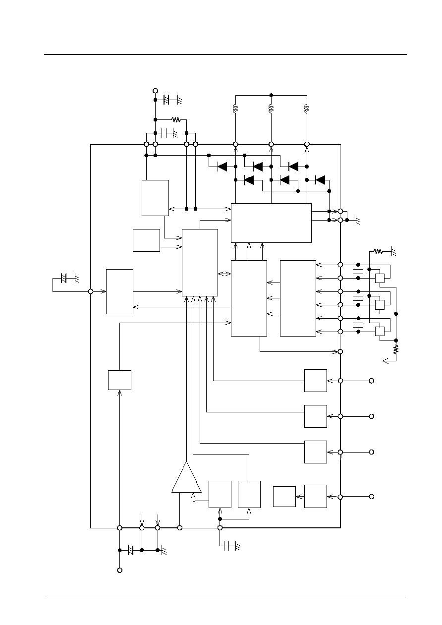
Overview
The LB11920 is a direct PWM drive motor driver IC for
3-phase power brushless motors. The PWM duty can be
controlled by IC inputs, and it can be used over the wide
supply voltage range of 9.5 to 30 V.
Functions and Features
∑ Three-phase bipolar drive (35 V, 3.5 A)
∑ Direct PWM drive
∑ Built-in high and low side kickback absorbing diodes
∑ Braking function (short-circuit braking)
∑ Built-in forward/reverse direction switching circuit
∑ Full complement of built-in protection circuits,
including current limiter, low-voltage protection, motor
lock (physical constraint) protection, and thermal
protection circuits
∑ The PWM duty can be controlled by IC inputs
Package Dimensions
unit: mm
3147C-DIP28H (500mil)
1
14
28
15
0.4
0.6
4.0
4.0
26.75
20.0
R1.7
8.4
(1.81)
1.78
1.0
12.7
11.2
SANYO: DIP-28H
[LB11920]
LB11920
SANYO Electric Co.,Ltd. Semiconductor Company
TOKYO OFFICE Tokyo Bldg., 1-10, 1 Chome, Ueno, Taito-ku, TOKYO, 110-8534 JAPAN
Three-Phase Brushless Motor Driver
for Office Equipment Applications
Monolithic Digital IC
Any and all SANYO products described or contained herein do not have specifications that can handle
applications that require extremely high levels of reliability, such as life-support systems, aircraft's
control systems, or other applications whose failure can be reasonably expected to result in serious
physical and/or material damage. Consult with your SANYO representative nearest you before using
any SANYO products described or contained herein in such applications.
SANYO assumes no responsibility for equipment failures that result from using products at values that
exceed, even momentarily, rated values (such as maximum ratings, operating condition ranges, or other
parameters) listed in products specifications of any and all SANYO products described or contained
herein.
Parameter
Symbol
Conditions
Ratings
Unit
Supply voltage 1
VM max
35
V
Supply voltage 2
V
CC
max
7
V
Output voltage
V
OUT
max
OUT1 to OUT3
35
V
Output current
I
O
max
T
500 ms
3.5
A
Allowable power dissipation 1
Pd max1
Independent IC
3
W
Allowable power dissipation 2
Pd max2
With an infinitely large heat sink.
20
W
Operating temperature
Topr
≠20 to +80
∞C
Storage temperature
Tstg
≠55 to +150
∞C
Specifications
Absolute Maximum Ratings
at Ta = 25∞C

No. 7229-2/10
LB11920
Parameter
Symbol
Conditions
Ratings
Unit
Supply voltage range 1
VM
9.5 to 30
V
Supply voltage range 2
V
CC
4.5 to 5.5
V
HP pin applied voltage
VHP
0 to 32
V
HP pin output current
IHP
0 to 3
mA
Allowable Operating Ranges
at Ta = 25∞C
Parameter
Symbol
Conditions
Ratings
Unit
min
typ
max
Supply current 1
IV
CC
-1
V
CC
pin
9
13
mA
Supply current 2
IV
CC
-2
V
CC
pin at stop mode
2.0
3.0
mA
[Output block]
Output saturation voltage 1
V
O
sat1
I
O
= 1.0 A, V
O
(SINK) + V
O
(SOURCE)
1.7
2.4
V
Output saturation voltage 2
V
O
sat2
I
O
= 2.0 A, V
O
(SINK) + V
O
(SOURCE)
2.0
2.9
V
Output saturation voltage 3
V
O
sat3
I
O
= 3.0 A, V
O
(SINK) + V
O
(SOURCE)
2.4
3.5
V
Output leakage current
I
O
leak
100
µA
Output delay time 1
td1
PWMIN "H"
"L"
1.25
2.5
µs
Output delay time 2
td2
PWMIN "L"
"H"
1.8
3.6
µs
Lower diode forward 1
VD1-1
ID = ≠1.0 A
1.1
1.5
V
Lower diode forward 2
VD1-2
ID = ≠2.0 A
1.3
1.9
V
Lower diode forward 3
VD1-3
ID = ≠3.0 A
1.5
2.3
V
Upper diode forward 1
VD2-1
ID = 1.0 A
1.3
1.7
V
Upper diode forward 2
VD2-2
ID = 2.0 A
2.0
2.7
V
Upper diode forward 3
VD2-3
ID = 3.0 A
2.7
3.7
V
[Hall Amplifier Block]
Input bias current
IHB
≠2
≠0.1
µA
Common-mode input voltage range 1
VICM1
Hall device used
0.5
V
CC
≠ 2.0
V
Common-mode input voltage range 2
VICM2
For input one-side bias (Hall IC application)
0
V
CC
V
Hall input sensitivity
at differential input
50
mVp-p
Hysteresis width
VIN
20
30
50
mV
Input voltage L
H
VSLH
5
15
25
mV
Input voltage H
L
VSHL
≠25
≠15
≠5
mV
[PWM oscillator]
Output H level voltage
V
OH
(PWM)
2.75
3.0
3.25
V
Output L level voltage
V
OL
(PWM)
1.0
1.2
1.3
V
External C charge current
ICHG (PWM)
VPWM = 2.1 V
≠60
≠45
≠30
µA
Oscillator frequency
f (PWM)
C = 1000 pF
15.8
20
24.2
kHz
Amplitude
V (PWM)
1.6
1.8
2.1
Vp-p
[CSD circuit]
Operating voltage
V
OH
(CSD)
3.6
3.9
4.2
V
External C charge current
ICHG (CSD)
VCSD = 0V
≠15
≠11
≠7
µA
Operating time
T (CSD)
C = 10 µF
*
Design target value
3.5
s
Electrical Characteristics
at Ta = 25∞C, VM = RF = 27 V, V
CC
= 5 V
Continued on next page.
Note:
*
This parameter is a design target value and is not measured.
No. 7229-3/10
LB11920
Continued from preceding page.
Parameter
Symbol
Conditions
Ratings
Unit
min
typ
max
[HP pin]
Output low level voltage
V
OL
(HP)
IHP = 2 mA
0.1
0.4
V
Output leakage current
Ileak (HP)
VHP = 30 V
10
µA
[Thermal shutdown operation]
Thermal shutdown operating temperature
TTSD
*
Design target value (junction temperature)
150
180
∞C
Hysteresis width
TSD
*
Design target value (junction temperature)
45
∞C
[Current limiter circuit(RF pin)]
Limiter voltage
VRF
0.45
0.5
0.55
V
[Low-voltage protection circuit]
Operating voltage
VSDL
3.6
3.8
4.0
V
Release voltage
VSDH
4.1
4.3
4.5
V
Hysteresis width
VSD
0.35
0.5
0.65
V
[PWMIN pin]
Input frequency
f (PI)
50
kHz
H level input voltage
V
IH
(PI)
2.0
V
CC
V
L level input voltage
V
IL
(PI)
0
1.0
V
Input open voltage
V
IO
(PI)
V
CC
≠ 0.5
V
CC
V
Hysteresis width
V
IS
(PI)
0.15
0.25
0.35
V
H level input current
I
IH
(PI)
VPWMIN = V
CC
≠10
0
10
µA
L level input current
I
IL
(PI)
VPWMIN = 0 V
≠116
≠87
≠58
µA
[S/S pin]
H level input voltage
V
IH
(SS)
2.0
V
CC
V
L level input voltage
V
IL
(SS)
0
1.0
V
Input open voltage
V
IO
(SS)
V
CC
≠ 0.5
V
CC
V
Hysteresis width
V
IS
(SS)
0.15
0.25
0.35
V
H level input current
I
IH
(SS)
VS/S = V
CC
≠10
0
10
µA
L level input current
I
IL
(SS)
VS/S = 0 V
≠116
≠87
≠58
µA
[F/R pin]
H level input voltage
V
IH
(FR)
2.0
V
CC
V
L level input voltage
V
IL
(FR)
0
1.0
V
Input open voltage
V
IO
(FR)
V
CC
≠ 0.5
V
CC
V
Hysteresis width
V
IS
(FR)
0.15
0.25
0.35
V
H level input current
I
IH
(FR)
VF/R = V
CC
≠10
0
10
µA
L level input current
I
IL
(FR)
VF/R = 0 V
≠116
≠87
≠58
µA
[BR pin]
H level input voltage
V
IH
(BR)
2.0
V
CC
V
L level input voltage
V
IL
(BR)
0
1.0
V
Input open voltage
V
IO
(BR)
V
CC
≠ 0.5
V
CC
V
Hysteresis width
V
IS
(BR)
0.15
0.25
0.35
V
H level input current
I
IH
(BR)
VBR = V
CC
≠10
0
10
µA
L level input current
I
IL
(BR)
VBR = 0 V
≠116
≠87
≠58
µA
Note:
*
This parameter is a design target value and is not measured.