 | –≠–ª–µ–∫—Ç—Ä–æ–Ω–Ω—ã–π –∫–æ–º–ø–æ–Ω–µ–Ω—Ç: LB11975 | –°–∫–∞—á–∞—Ç—å:  PDF PDF  ZIP ZIP |

Ordering number : ENN6497A
11201RM (OT) No. 6497-1/12
Overview
The LB11975 is a monolithic bipolar IC developed for
uses as a spindle motor driver for high-speed CD-ROM
and DVD-ROM drives. To minimize heat generation
during high-speed rotation and braking, the LB11975
adopts direct PWM drive in the output stage. During
reverse braking the upper and lower side output transistors
are both driven in PWM mode to implement dual PWM
controlled braking. The device thus controls the current to
remain under a limit value and prevent rapid heat
generation. This prevents device destruction due to rapid
heating. The absolute maximum voltage rating is 27 V,
and the maximum current is 2.5 A.
Functions and Features
∑ Direct PWM drive (lower side control)
∑ Built-in upper and lower side output diodes
∑ Supports the use 3.3 V DSP devices.
∑ Power saving function for standby mode
∑ Hall FG output (1 or 3 Hall device operation)
∑ Built-in Hall device power supply
∑ Reverse rotation detection output and drive cutoff circuit
∑ Voltage control amplifier
∑ Current limiter circuit
∑ Thermal protection circuit
Package Dimensions
unit: mm
3251-HSOP36R
(6.2)
36
1
19
18
0.8
2.0
17.8
0.3
(4.9)
2.7
0.65
0.25
(0.5)
7.9
10.5
2.25
2.45max
0.1
SANYO: HSOP36R
[LB11975]
LB11975
SANYO Electric Co.,Ltd. Semiconductor Company
TOKYO OFFICE Tokyo Bldg., 1-10, 1 Chome, Ueno, Taito-ku, TOKYO, 110-8534 JAPAN
High-Speed CD-ROM Spindle Motor Driver IC
Monolithic Digital IC
Any and all SANYO products described or contained herein do not have specifications that can handle
applications that require extremely high levels of reliability, such as life-support systems, aircraft's
control systems, or other applications whose failure can be reasonably expected to result in serious
physical and/or material damage. Consult with your SANYO representative nearest you before using
any SANYO products described or contained herein in such applications.
SANYO assumes no responsibility for equipment failures that result from using products at values that
exceed, even momentarily, rated values (such as maximum ratings, operating condition ranges, or other
parameters) listed in products specifications of any and all SANYO products described or contained
herein.
0.4
0
0.8
0.9
1.2
1.6
2.0
2.1
2.4
≠20
0
20
40
60
80
100
Allowable power dissipation, Pd max -- W
Pd max -- Ta
Ambient temperature, Ta --
∞
C
Mounted on the specified printed circuit
(114.3
◊
76.1
◊
1.6 mm
3
glass epoxy board)
Independent IC
0.54
1.26
No. 6497-2/12
LB11975
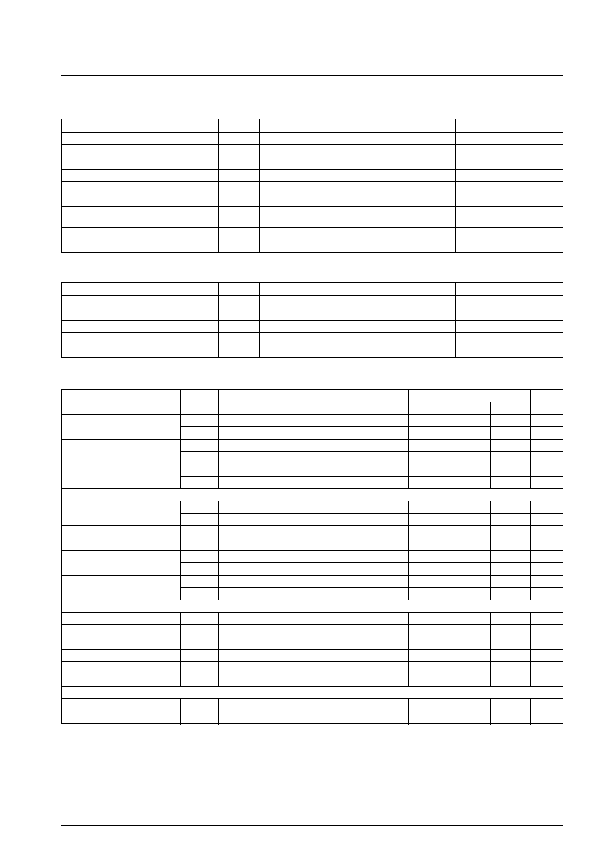
Parameter
Symbol
Conditions
Ratings
Unit
Supply voltage 1
V
CC
1 max
7
V
Supply voltage 2
V
CC
2 max
27
V
Supply voltage 3
V
CC
3 max
27
V
Output current
I
O
max
2.5
A
Output applied voltage
V
IN
max
30
V
Allowable power dissipation 1
Pd max1
Independent IC
0.9
W
Allowable power dissipation 2
Pd max2
Mounted on the specified circuit board
2.1
W
(114.3
◊
76.1
◊
1.6 mm
3
glass epoxy board)
Operating temperature
Topr
≠20 to +75
∞C
Storage temperature
Tstg
≠55 to +150
∞C
Specifications
Maximum Ratings
at Ta = 25∞C
Parameter
Symbol
Conditions
Ratings
Unit
Power-supply voltage range 1
V
CC
1
4 to 6
V
Power-supply voltage range 2
V
CC
2
V
CC
2
V
CC
1
4 to 16
V
Power-supply voltage range 3
V
CC
3
4 to 16
V
FG pin applied voltage
VFG
0 to V
CC
1
V
FG pin output current
IFG
0 to 4.0
mA
Allowable Operating Ranges
at Ta = 25∞C
Parameter
Symbol
Conditions
Ratings
Unit
min
typ
max
Supply current 1
I
CC
1-1
V
CTL
= V
CREF
5.0
8.0
11.0
mA
I
CC
1-2
VS/S = 0 V
0
200
µA
Supply current 2
I
CC
2-1
V
CTL
= V
CREF
5.0
6.5
8.0
mA
I
CC
2-2
VS/S = 0 V
0
200
µA
Supply current 3
I
CC
3-1
V
CTL
= V
CREF
0.3
0.7
mA
I
CC
3-2
VS/S = 0 V
0
200
µA
[Output Block]
Output saturation voltage 1
V
O
sat1(L) I
O
= 0.5 A, V
O
(sink), V
CC
1 = 5 V, V
CC
2 = V
CC
3 = 12 V
0.15
0.25
V
V
O
sat1(H) I
O
= 0.5 A, V
O
(source), V
CC
1 = 5 V, V
CC
2 = V
CC
3 = 12 V
0.80
0.95
V
Output saturation voltage 2
V
O
sat2(L) I
O
= 1.5 A, V
O
(sink), V
CC
1 = 5 V, V
CC
2 = V
CC
3 = 12 V
0.40
0.60
V
V
O
sat2(H) I
O
= 1.5 A, V
O
(source), V
CC
1 = 5 V, V
CC
2 = V
CC
3 = 12 V
1.10
1.30
V
Output leakage current
I
O
leak(L)
100
µA
I
O
leak(H)
≠100
µA
Diode forward voltage
V
F
H
Upper side diode, I
O
= 2.0 A
1.50
2.00
V
V
F
L
Lower side diode, I
O
= 2.0 A
1.50
2.00
V
[Hall Amplifier Block]
Input bias current
I
HB
≠4
≠1
µA
Common-mode input voltage range
V
ICM
1.5
V
CC
≠ 1.5
V
Hall input sensitivity
V
HIN
60
mVp-p
Hysteresis
V
IN
(HA)
23
32
39
mV
Input voltage: low
high
V
SL
H
6
16
25
mV
Input voltage: high
low
V
SL
L
≠25
≠16
≠6
mV
[Thermal Protection Circuit]
Operating temperature
T-TSD
Design target value (junction temperature)
*
150
180
210
∞C
Hysteresis
TSD
Design target value (junction temperature)
*
40
∞C
Electrical Characteristics
at Ta = 25∞C, V
CC
1 = 5 V, V
CC
2 = V
S
= 12 V
Continued on next page.
Note:
*
These are design target values and are not tested.

No. 6497-3/12
LB11975
Continued from preceding page.
Parameter
Symbol
Conditions
Ratings
Unit
min
typ
max
[PWM Oscillator]
High-level output voltage
V
O
H(OSC)
3.1
3.3
3.5
V
Low-level output voltage
V
O
L(OSC)
1.4
1.6
1.8
V
Amplitude
V(OSC)
1.5
1.7
1.9
Vp-p
Oscillator frequency
f(OSC)
C = 2200 pF
23.0
kHz
Charge current
I
CHG
≠110
≠94
≠83
µA
Charge resistor value
R
DCHG
1.6
2.1
2.6
k
[CTL Amplifier]
VCTL pin input current
I
VCTL
V
CTL
= V
CREF
= 1.65 V
≠2
µA
VCREF pin input current
I
VCREF
V
CTL
= V
CREF
= 1.65 V
≠2
µA
Forward rotation gain
GDF
+
Design target value
*
0.20
0.25
0.30
times
Reverse rotation gain
GDF
≠
Design target value
*
≠0.30
≠0.25
≠0.20
times
Forward rotation limiter voltage
V
RF
1
0.26
0.29
0.32
V
Reverse rotation limiter voltage
V
RF
2
0.26
0.29
0.32
V
Startup voltage
V
CTH
V
CREF
= 1.65 V. Design target value
*
1.50
1.80
V
Dead zone
V
DZ
V
CREF
= 1.65 V. Design target value
*
35
80
140
mV
[FG Pin] (speed pulse output)
Low-level output voltage
V
FGL
I
FG
= 2 mA
0.4
V
Pull-up resistor value
R
FG
7.5
10
12.5
k
[RS Pin]
Low-level output voltage
V
RSL
I
RS
= 2 mA
0.4
V
Pull-up resistor value
R
RS
7.5
10
12.5
k
[Stop/Start Pin]
Low-level input voltage
V
SS
L
0
0.7
V
High-level input voltage
V
SS
H
2.0
V
CC
1
V
Low-level input current
I
SS
L
V
SS
= 0 V
≠1
0
µA
High-level input current
I
SS
H
V
SS
= 5.0 V
50
200
µA
[Hall Device Power Supply]
Hall device supply voltage
V
H
I
H
= 5 mA
0.65
0.85
1.05
V
Allowable current
I
H
20
mA
Truth Table
Input
Control voltage V
CTL
Output
FG output
IN1
IN2
IN3
Source
Sink
FG1
FG2
1
H
L
H
H
OUT2
OUT1
L
H
L
OUT1
OUT2
2
H
L
L
H
OUT3
OUT1
L
L
L
OUT1
OUT3
3
H
H
L
H
OUT3
OUT2
L
H
L
OUT2
OUT3
4
L
H
L
H
OUT1
OUT2
H
L
L
OUT2
OUT1
5
L
H
H
H
OUT1
OUT3
H
H
L
OUT3
OUT1
6
L
L
H
H
OUT2
OUT3
H
L
L
OUT3
OUT2
Note:
*
These are design target values and are not tested.
FG1
FG2

Block Diagram
No. 6497-4/12
LB11975
23
IN1
+
IN1
≠
IN2
≠
IN3
≠
IN2
+
IN3
+
28
9
15
22
21
20
19
18
MATRIX
&
LOGIC
TSD
V
CC
3
OSC
Rotation direction
detection
S/S
16
27
HALL
BIAS
CURR
LIM
14
13
12
PH
11
10
PWM
FC
V
CREF
V
CTL
GND1
(7, 30, 31)
GND2
(4)
OUT3
(2)
OUT2
(36)
OUT1
Rf
V
CC
2
(29)
V
CC
3
V
CC
1
VH
S/S
25
FG2
26
FG1
24
RS
A13185
8
35
1
3
6
17

Pin Assignment
No. 6497-5/12
LB11975
1
FR
FR
IN1+
RS
FG2
VCC1
FG1
RF
GND2
GND2
OUT1
VCC3
OUT1
IN2-
IN3+
FRAME
GND
IN2+
IN1-
GND2
OUT2
IN3-
FRAME
GND
GND1
VCTL
VCREF
PH
VH
S/S
OUT3
NC
NC
NC
NC
VCC2
GND2
OUT3
OUT2
FC
PWM
VCC3
LB11975
2
3
4
5
6
7
8
9
10
11
12
13
14
15
16
17
18
36
35
34
33
32
31
30
29
28
27
26
25
24
23
22
21
20
19
Top view
Sample Application Circuit
No. 6497-6/12
LB11975
23
0.01
µ
F
0.01
µ
F
0.01
µ
F
0.01
µ
F
1.65V
2200pF
IN1
+
IN1
≠
IN2
≠
IN3
≠
IN2
+
IN3
+
H
28
9
15
22
21
20
19
18
V
CC
1
10k
◊
3
MATRIX
&
LOGIC
TSD
V
CC
3
OSC
Rotation direction
detection
S/S
16
27
HALL
BIAS
CURR
LIM
14
13
12
PH
11
10
PWM
FC
V
CREF
V
CTL
GND1
GND2
OUT3
OUT2
OUT1
Rf
C
V
CC
2
V
CC
3
V
CC
1
VH
S/S
25
FG2
26
FG1
24
RS
H
H
A13186
8
35
1
3
6
17

No. 6497-7/12
LB11975
Pin Functions
Pin No.
Pin
Pin voltage
Function
Equivalent circuit
4 V to 16 V
Supplies the source side pre-drive
voltage.
9
V
CC
2
24
10k
VCC1
25 26
21
23
19
20
22
500
500
VCC1
18
16
2k
30k
VCC1
4 V to 16 V
Supplies the motor drive voltage.
8
29
V
CC
3
4 V to 16 V
Supply voltage for all circuits other than
the output transistors and the source side
pre-drive voltage
27
V
CC
1
Reverse rotation detection
High-level output: Forward rotation
Low-level output: Reverse rotation
24
RS
Single Hall device waveform Schmitt
comparator synthesized output
26
FG1
Three Hall device waveform Schmitt
comparator synthesized output
25
FG2
U phase Hall device input.
Logic high refers to the state where IN1
+
> IN1
≠
.
23
IN1
+
1.5 V to
V
CC
1 ≠ 1.5 V
V phase Hall device input.
Logic high refers to the state where IN2
+
> IN2
≠
.
W phase Hall device input.
Logic high refers to the state where IN3
+
> IN3
≠
.
Provides the Hall device lower side bias
voltage.
22
IN1
≠
21
IN2
+
20
IN2
≠
19
IN3
+
18
IN3
≠
16
VH
15
75k
50k
VCC1
All circuits can be set to the non-operating
state by setting this pin to 0.7 V or under,
or by setting it to the open state.
This pin must be held at 2 V or higher.
15
S/S
0 V to V
CC
1
Ground for all circuits except the output
17
GND1
Continued on next page.

No. 6497-8/12
LB11975
Continued from preceding page.
Pin No.
Pin
Pin voltage
Function
Equivalent circuit
Control loop frequency characteristics
correction
Closed loop oscillation in the current
control system can be stopped by
connecting a capacitor between this pin
and ground.
11
FC
11
10
VCC1
500
500
65k
500
2k
VCC1
13
14
500
500
28
2k
2k
VCC2
2
1
3
6
VCC1
VCC3
7
30 31
4
35 36
VCC1
300
12
11k
PWM oscillator capacitor connection
10
PWM
Control reference voltage input
The control start voltage is determined by
this voltage.
13
V
CREF
0 V to
V
CC
1 ≠ 1.5 V
Speed control voltage input
This IC implements a voltage control
system in which VC > V
CREF
means
forward rotation and VC < V
CREF
means
slow foward rotation.
(This IC includes reverse rotation
prevention circuit, so reverse rotation will
not occur.)
14
V
CTL
0 V to
V
CC
1 ≠ 1.5 V
W phase output
3, 4
OUT3
Ground for the output transistors
6, 7
30, 31
GND2
V phase output
1, 2
OUT2
U phase output
35, 36
OUT1
Upper side npn transistor collector
(shared by all three phases)
Connect a resistor between V
CC
3 and the
RF pin for current detection. The fixed
current control system and the current
limiter operate by detecting this voltage.
28
RF
Peak hold circuit capacitor connection.
Connect a capacitor to this pin to smooth
the voltage detected by the resistor RF.
12
PH

Torque Command
Figure 1 shows the relationship between the control voltage (V
CTL
) and the RF voltage.
No. 6497-9/12
LB11975
3mV
VRF
Forward rotation
1.65V
Dead zone
VCTL
VCREF=1.65V
Offset voltage
D
CK
Q
R
D
CK
Q
R
D
CK
Q
R
VCTL
VCREF
IN1+
IN1≠
IN2+
IN2≠
IN3+
IN3≠
OUT
Figure 1
Figure 2 Reverse Rotation Detection Circuit Block Diagram
Truth Table
Note:
*
Since this IC includes a reverse rotation prevention circuit, although the IC will brake the motor if the motor is rotating and V
CTL
< V
CREF
, when
reverse rotation is detected, the IC will turn the output off, thus stopping motor rotation.
Operation
V
CTL
> V
CREF
Forward rotation
V
CREF
> V
CTL
Reverse torque braking
*
Reverse Rotation Detection Circuit Truth Table
During forward rotation:
The OUT signal is set high to reset DFF.
During reverse rotation:
Reverse rotation is detected when the Hall comparator output falls.
At that point the OUT signal is set to the low level.
RS pin
Forward rotation
HIGH
Reverse rotation
LOW

Overview of Reverse Torque Braking
(This circuit uses a direct PWM drive technique and allows the current limiter to operate during reverse torque braking.)
In earlier direct PWM motor drivers, speed control was implemented by applying PWM to only one (either the upper or
lower) output transistor. With this type of driver, the regenerative current formed during reverse torque braking operated
as a short-circuit braking. As a result problems such as the coil current exceeding the limit value and I
O
max being
exceeded, would occur. To prevent these problems, the LB11975 switches both the upper and lower side output
transistors during reverse torque braking to suppress the generation of overcurrents due to regenerative currents when the
PWM is off and allows the optimal design of drive currents.
Supplementary Documentation
Coil current during reverse torque braking
(1) Earlier ICs, with the lower side transistor was switched and the upper side transistor used for current detection (RF)
During reverse torque braking, when the coil current increases and the limit is reached, the lower side output
transistor is turned off. At this time the regenerative current flows through the upper side transistor. The circuit path is
as follows:
Coil
upper side diode
V
CC
RF
upper side transistor
coil
During regeneration, the upper side transistor is on and the back EMF that occurs at the upper side transistor's emitter
pin has a low potential, and since the upper side transistor is fully on at that point, the circuit functions as short-circuit
braking.
Even if the regenerative current results in the RF voltage reaching the limit voltage, since the upper side transistor
cannot be turned off, the limit circuit will not operate and a coil current in excess of I
O
max may occur.
(2) Earlier ICs, with the upper side transistor was switched and the upper side transistor used for current detection (RF)
During reverse torque braking, when the coil current increases and the limit is reached, the upper side output
transistor is turned off. At this time the regenerative current flows through the lower side transistor. The circuit path is
as follows:
Coil
lower side transistor
ground
lower side diode
coil
During regeneration, the lower side transistor is on and the back EMF that occurs at the lower side transistor's
collector pin has a high potential, and since the lower side transistor is fully on at that point, the circuit functions as
short-circuit braking.
Since the regenerative current does not flow through the RF pin, the current limiter circuit does not operate, and a
current in excess of I
O
max may occur in the lower side transistor.
No. 6497-10/12
LB11975
IN1
IN2
IN3
Reverse rotation is detected with this timing.
Hall comparator
(IN1, IN2, and IN3)
waveforms
Figure 3 Reverse Rotation Timing Chart

(3) When both the upper and lower side transistors are switched and current detection (RF) is performed in the upper side
transistor
During reverse torque braking, when the coil current increases and the limit is reached, both the upper and lower side
transistors are turned off. The motor current circuit path at this point is as follows:
Coil
upper side diode
V
CC
power supply line capacitor
ground
lower side diode
coil
When the limiter circuit operates, both the upper and lower side transistors are turned off, so short-circuit breaking
does not occur, and coil current attenuation is all that occurs. Thus this technique allows current control at the set
(limiter) current to be performed even during reverse torque braking.
Regenerative Current Path
No. 6497-11/12
LB11975
≠
+
RF
A13187
Drive Mode

PS No. 6497-12/12
LB11975
This catalog provides information as of January, 2001. Specifications and information herein are subject
to change without notice.
Specifications of any and all SANYO products described or contained herein stipulate the performance,
characteristics, and functions of the described products in the independent state, and are not guarantees
of the performance, characteristics, and functions of the described products as mounted in the customer's
products or equipment. To verify symptoms and states that cannot be evaluated in an independent device,
the customer should always evaluate and test devices mounted in the customer's products or equipment.
SANYO Electric Co., Ltd. strives to supply high-quality high-reliability products. However, any and all
semiconductor products fail with some probability. It is possible that these probabilistic failures could
give rise to accidents or events that could endanger human lives, that could give rise to smoke or fire,
or that could cause damage to other property. When designing equipment, adopt safety measures so
that these kinds of accidents or events cannot occur. Such measures include but are not limited to protective
circuits and error prevention circuits for safe design, redundant design, and structural design.
In the event that any or all SANYO products (including technical data, services) described or contained
herein are controlled under any of applicable local export control laws and regulations, such products must
not be exported without obtaining the export license from the authorities concerned in accordance with the
above law.
No part of this publication may be reproduced or transmitted in any form or by any means, electronic or
mechanical, including photocopying and recording, or any information storage or retrieval system,
or otherwise, without the prior written permission of SANYO Electric Co., Ltd.
Any and all information described or contained herein are subject to change without notice due to
product/technology improvement, etc. When designing equipment, refer to the "Delivery Specification"
for the SANYO product that you intend to use.
Information (including circuit diagrams and circuit parameters) herein is for example only; it is not
guaranteed for volume production. SANYO believes information herein is accurate and reliable, but
no guarantees are made or implied regarding its use or any infringements of intellectual property rights
or other rights of third parties.
Braking Mode